

Page 1

DATA SHEET
BIPOLAR ANALOG INTEGRATED CIRCUIT
µ
PC1851B
I2C BUS-COMPATIBLE US MTS PROCESSING LSI
The µPC1851B is an integrated circuit for US MTS (Multiplexed Television Sound) system with the addition of
2
C bus interface. All functions required for US MTS system are incorporated on a single chip.
the I
The µPC1851B allows users to switch modes, control volume and tone, and adjust the separation circuit
through the I2C bus.
FEATURES
• Stereo demodulation, SAP (Sub Audio Program) demodulation, dbx noise reduction decoding, I2C bus interface,
input selector (2 channels), surround processor (1 phase), volume and tone control circuits incorporated on a single
chip
2
• Mode switching, volume and tone control, and separation adjustment through the I
• Power supply: 8 V to 10 V
• On-chip input attenuator for simple interface with intermediate frequency processing IC (I
• Output level: 1.4 Vp-p (with L+R signals, 100 % modulation)
C bus
2
C bus control)
APPLICATION
• TV sets and VCRs for north America
ORDERING INFORMATION
Part Number Package
µ
PC1851BCU 42-pin plastic SDIP (15.24 mm (600))
The µPC1851B is available only to licensees of THAT Corporation.
For information, please call: (508) 229-2500 (U.S.A), or (03) 5790-5391 (Tokyo).
The information in this document is subject to change without notice. Before using this document, please
confirm that this is the latest version.
Not all devices/types available in every country. Please check with local NEC representative for availability
and additional information.
Document No. S13417EJ2V0DS00 (2nd edition)
Date Published June 2000 N CP(K)
Printed in Japan
The mark shows major revised points.
©
1998
Page 2
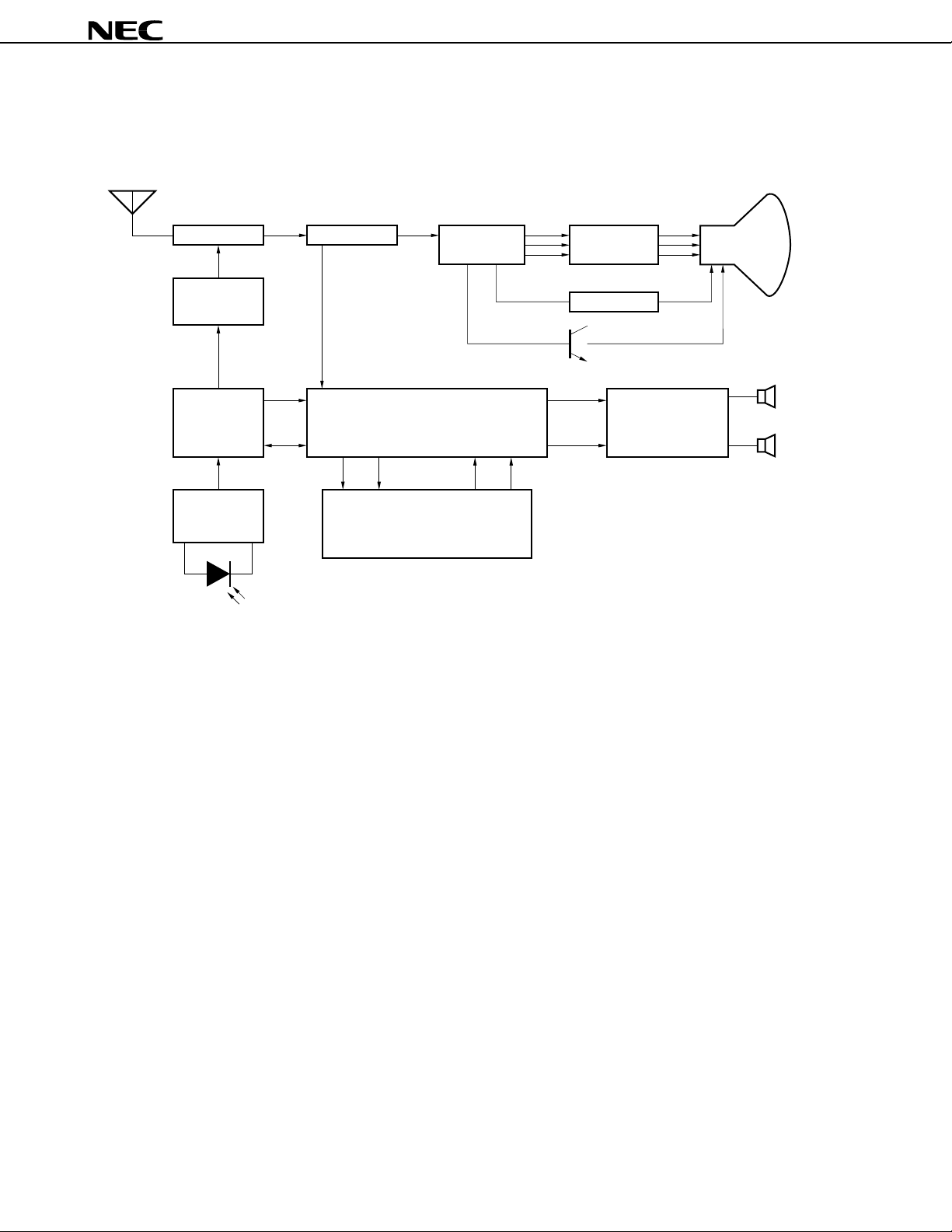
SYSTEM BLOCK DIAGRAM
● TV
µ
PC1851B
Tuner
DTS
interface
Tuning
microcontroller
Remote
controller
receive amp.
PIN photodiode
IF processing
PC1851B
µ
SCL
MTS processing
SDA R
LLRR
Graphic equalizer
(Surround processor)
C, Y, and
deflecting
signal output
Chroma output
Vertical output
L
Power amplifier
CRT
2
Data Sheet S13417EJ2V0DS00
Page 3
µ
PC1851B
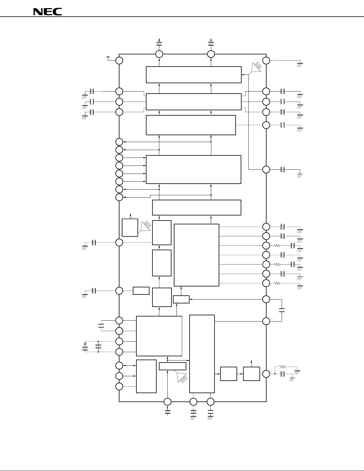
BLOCK DIAGRAM
µ
2.2 F
+
2200 pF
0.1 F
µ
+
9 V
V
TLO
LTC
LBC
FOR
FOL
EL2
EL1
ER2
ER1
MOL
MOR
10 F
+
LOT
26
1
CC
ROT
25
10 F
µµ
+
21
AGND
D/A
Volume Control
2.2 F
µ
31
32
33
Tone Control
Surround Block
28
29
30
27
TRO
RTC
RBC
SUR
+
2200 pF
0.1 F
µ
+
0.022 F
µ
40
41
37
4.7 F
VOL-C
µ
+
39
36
Selector Block
19
38
35
34
Filter
Matrix Block
1 kΩ
+
4.7 F
22 F
0.1 F
µ
1 F
µ
µ
µ
1 F
µ
+
+
+
DGND
MOA
VRE
PD2
PD1
φ
D1
φ
D2
SDA
SCL
42
2
4
3
5
6
22
23
24
Filter
Control
D/A
1/2V
I2C Bus
Interface
CC
Offset
Absorption
De-
emphasis
L+R
LPF
Stereo
Demodulation
Block
Input Attenuator
dbx Noise
Reduction Block
Switch
Demodulation
D/A
SAP
Block
Noise
BPF
I2C Bus
Interface
Noise
Detector
20
16
17
13
14
18
15
11
10
µ
1 F
VOA
10 F
µ
WTI**
WRB
STI**
SRB
dO
5.1 kΩ
3.3 F
+++
3 kΩ
1 F
+
16.6 kΩ
µ
1 F
+
µ
µ
1
F
+
µ
ITI*
SI
µ
0.1
F
SOT
68 k
Ω
+
9
NDT
µ
0.47 F
COM
7
+
2.2 F
SOA
12
SDT
+
0.1 F
8
0.047 F
µ µ µ
Remark Use the followings for external parts.
Resistor (*): Metal film resistor (± 1 %). Unless otherwise specified; ±5 %
Capacitors (**): Tantalum capacitor (±10 %). Unless otherwise specified; ±20 %
Data Sheet S13417EJ2V0DS00
3
Page 4
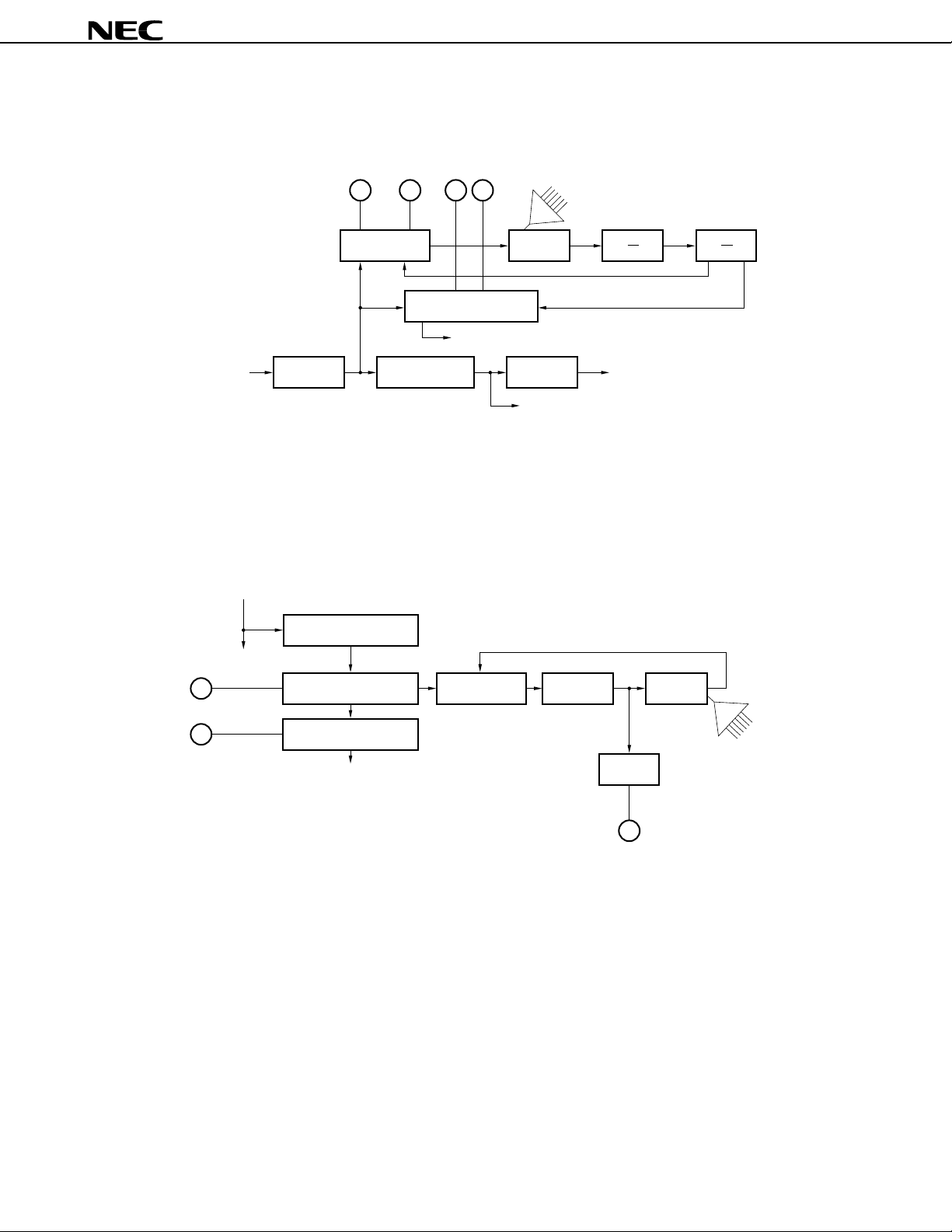
STEREO DEMODULATION BLOCK
D2
φ
D1
φ
5
Stereo Phase
Comparator
6
PD14PD2
3
Pilot Discrimination
Phase Comparator
2
C bus Interface
To I
D/A
Stereo
VCO
µ
PC1851B
Divider
1
4
1
2
From Input Attenuator
Stereo LPF
SAP DEMODULATION BLOCK
From Input Attenuator
To Noise BPF
SOA
12
8SDT
Offset Absorption
To I2C bus Interface
SAP BPF
SAP Detector
Pilot Canceler
Phase Detector
L–R AM
Demodulator
To L+R LPF
Loop Filter SAP VCO
To Switch
SAP LPF
D/A
10
SOT
4
Data Sheet S13417EJ2V0DS00
Page 5
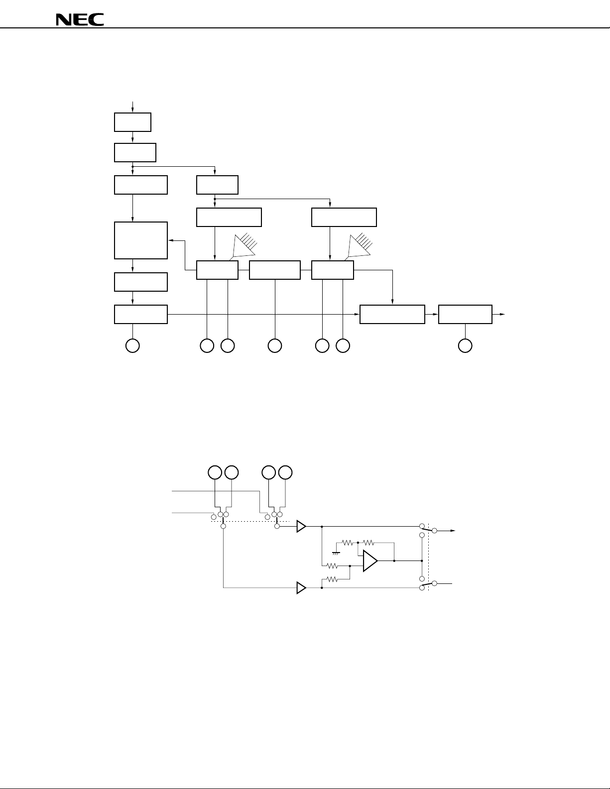
dbx NOISE REDUCTION BLOCK
From Switch
LPF
fH Trap
µ
PC1851B
408-Hz LPF
Variable
Emphasis
2.19-kHz LPF
Offset
Absorption
18
dO
SELECTOR BLOCK
2 fH Trap
Spectral RMS Filter
Spectral
RMS
14
SRB13STI
ER136ER2
38
Timing Current
15
ITI
EL137EL2
39
Wide-band RMS
Filter
D/AD/A
Wide-band
RMS
Wide-band VCA
16
17
WTI
WRB
Offset
Absorption
20
VOA
To Matrix Block
From Matrix Block
(L-channel signal)
From Matrix Block
(R-channel signal)
Switch
Note1
Note2
Note2
40 kΩ 40 kΩ
40 kΩ
40 kΩ
Notes 1. Switch (TV signal/External input 1/External input 2).
2. The input gain 0 dB/6 dB can be selected by the command of the I
Data Sheet S13417EJ2V0DS00
To Surround Block
–
+
2
C bus (refer to 4.3 (5) Input gain).
Switch (Monaural/Stereo)
To Surround Block
5
Page 6
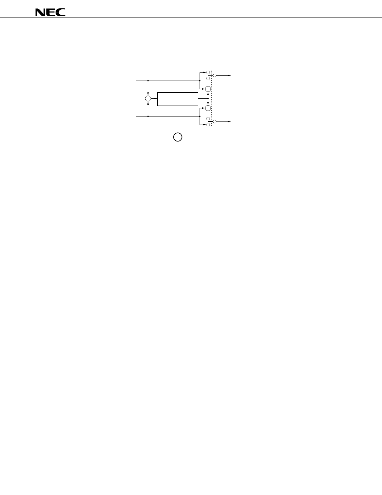
SURROUND BLOCK
µ
PC1851B
From Selector Block
(L-channel)
From Selector Block
(R-channel)
–
To Tone Control Block
–
Phase Shifter
+
To Tone Control Block
27
SUR
6
Data Sheet S13417EJ2V0DS00
Page 7
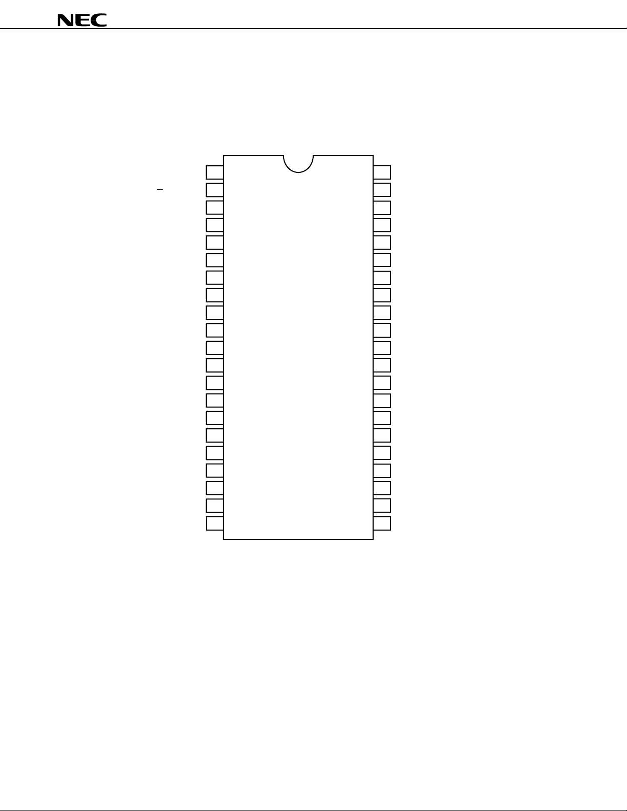
PIN CONFIGURATION (Top View)
42-pin plastic SDIP (15.24 mm (600))
• µPC1851BCU
µ
PC1851B
Power Supply (9 V)
1
Vcc Filter
2
Pilot Discrimination Filter 1
Pilot Discrimination Filter 2
Phase Comparator Filter 1
Phase Comparator Filter 2
Composite Signal Input
SAP Discrimination Filter
Noise Detector Filter
SAP Single Output
SAP Single Input
SAP Offset Absorption
Spectral RMS Timing
Spectral RMS Offset Absorption
Timing Current Setting
Wide-band RMS Timing
Wide-band RMS Offset Absorption
10
11
12
13
14
15
16
17
V
CC
1
VRE
2
PD1
3
PD2
4
φ
D1
5
φ
D2
6
COM
7
SDT
8
NDT
9
SOT
SI
SOA
STI
SRB
ITI
WTI
WRB
MOA
FOL
FOR
EL1
ER1
EL2
ER2
MOL
MOR
LBC
LTC
TLO
RBC
RTC
TRO
SUR
LOT
42
Monaural Offset Absorption
41
L-channel Fixed Output
40
R-channel Fixed Output
39
External L-channel Input 1
38
External R-channel Input 1
37
External L-channel Input 2
36
External R-channel Input 2
35
L-channel Matrix Output
34
R-channel Matrix Output
33
L-channel Capacity of Low Frequency Band Width
32
L-channel Capacity of High Frequency Band Width
31
L-channel Offset Absorption
30
R-channel Capacity of Low Frequency Band Width
29
R-channel Capacity of High Frequency Band Width
28
R-channel Offset Absorption
27
Surround Timing
26
L-channel Output
Variable Emphasis Offset Absorption
Volume Control Offset Absorption
VCA Offset Absorption
Analog GND
18
19
20
21
dO
VOL-C
VOA
AGND
ROT
DGND
SCL
SDA
25
R-channel Output
24
Digital GND (for I
SCL (for I
23
SDA (for I
22
2
C bus)
2
C bus)
2
C bus)
Data Sheet S13417EJ2V0DS00
7
Page 8

CONTENTS
1. PIN EQUIVALENT CIRCUITS............................................................................................ 9
2. BLOCK FUNCTIONS........................................................................................................ 18
2.1 Stereo Demodulation Block................................................................................... 18
2.2 SAP Demodulation Block ...................................................................................... 19
2.3 dbx Noise Reduction Block ................................................................................... 20
2.4 Matrix Block............................................................................................................ 21
2.5 Selector Block ........................................................................................................ 21
2
C BUS INTERFACE ....................................................................................................... 22
3. I
3.1 Data Transfer ......................................................................................................... 23
3.2 Data Transfer Format ............................................................................................ 24
2
C BUS COMMANDS ...................................................................................................... 27
4. I
4.1 Subaddress List ..................................................................................................... 27
4.2 Setting Procedure .................................................................................................. 29
4.3 Explanation of Write Register ................................................................................ 31
4.4 Explanation of Read Register ............................................................................... 38
µ
PC1851B
5. MODE MATRIX ................................................................................................................. 4 0
6. SELECTOR TABLE.......................................................................................................... 41
7. USAGE CAUTIONS.......................................................................................................... 42
7.1 Caution on Shock Noise Reduction ...................................................................... 42
7.2 Supply Voltage....................................................................................................... 42
7.3 Impedance of Input and Output Pins .................................................................... 42
7.4 Drive Capability of Output Pins ............................................................................. 42
7.5 Caution on External Components ......................................................................... 43
7.6 Change of Electrical Characteristics by External Components........................... 43
8. ELECTRICAL SPECIFICATIONS.................................................................................... 44
9. TEST CIRCUIT.................................................................................................................. 56
10. PACKAGE DRAWINGS ................................................................................................... 58
11. RECOMMENDED SOLDERING CONDITIONS .............................................................. 59
8
Data Sheet S13417EJ2V0DS00
Page 9
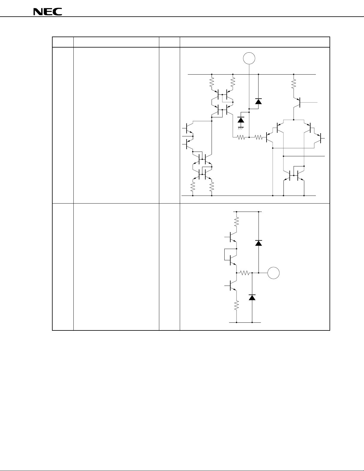
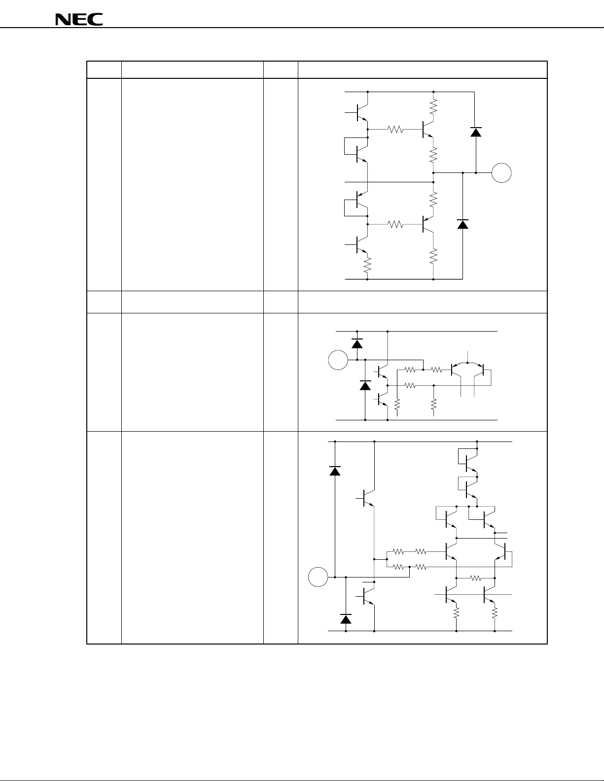
1. PIN EQUIVALENT CIRCUITS
Pin No. Pin Name Symbol Internal Equivalent Circuit
1 Power Supply (9 V) VCC
µ
PC1851B
(1/9)
1
2 VCC Filter VRE
2
3 Pilot Discrimination Filter 1 PD1
VCC
10 kΩ 10 kΩ
5 kΩ
20 kΩ
20 kΩ
20 kΩ
10 kΩ
2
10 kΩ
20 kΩ
5 kΩ
GND
V
CC
3
15 kΩ 5 kΩ
15 kΩ
4 Pilot Discrimination Filter 2 PD2
1
CC
V
2
V
CC
4
15 kΩ15 kΩ 5 kΩ
Data Sheet S13417EJ2V0DS00
9
Page 10
Pin No. Pin Name Symbol Internal Equivalent Circuit
µ
PC1851B
(2/9)
5 Phase Comparator Filter 1
6 Phase Comparator Filter 2
φ
D1
φ
D2
7 Composite Signal Input COM
V
CC
5
15 kΩ 5 kΩ
V
CC
6
1
V
CC
2
5 kΩ
5 kΩ15 kΩ 5 kΩ
1
V
CC
2
CC
V
80 kΩ
7
3 kΩ
17 kΩ
8 SAP Discrimination Filter SDT
5 kΩ 5 kΩ
GND
8
VCC
20 kΩ
10 kΩ
20 kΩ20 kΩ
10 kΩ
GND
10
Data Sheet S13417EJ2V0DS00
Page 11
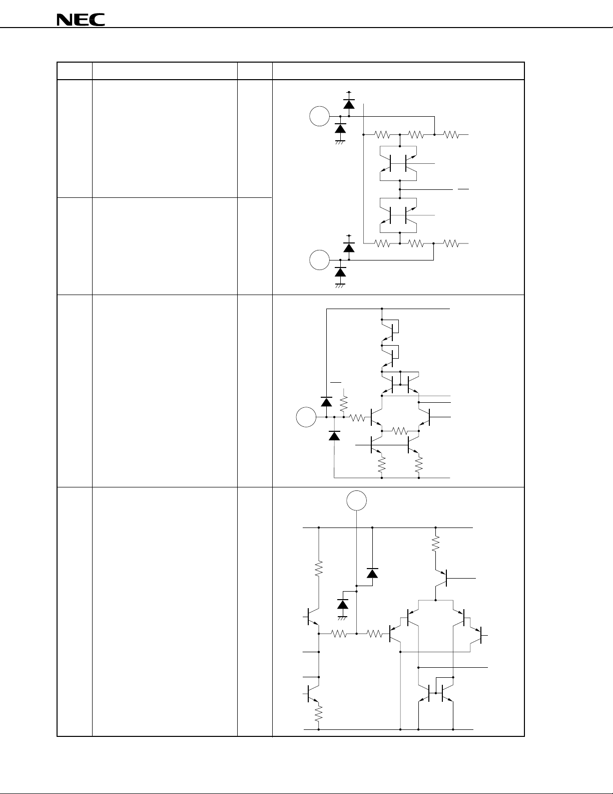
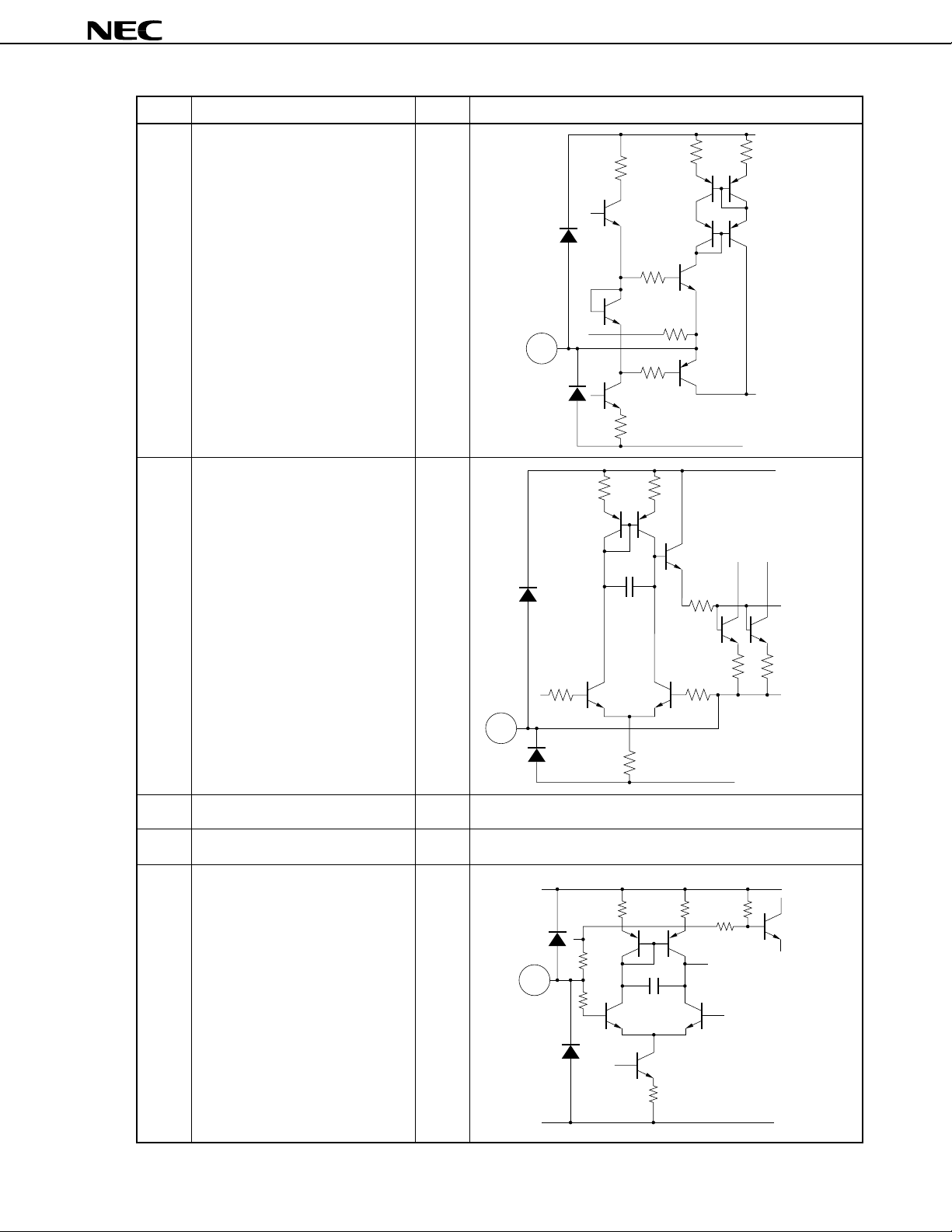
Pin No. Pin Name Symbol Internal Equivalent Circuit
µ
PC1851B
(3/9)
9 Noise Detector Filter NDT
10 SAP Single Output SOT
20 kΩ20 kΩ
20 kΩ 20 kΩ
2 kΩ
9
V
CC
20 kΩ
20 kΩ20 kΩ
GND
V
CC
2 kΩ
200 Ω
10
GND
Data Sheet S13417EJ2V0DS00
11
Page 12
Pin No. Pin Name Symbol Internal Equivalent Circuit
11 SAP Single Input SI
10 kΩ 10 kΩ
80 kΩ
11
5 kΩ
5 pF
5 kΩ
1
2
V
CC
GND
µ
V
CC
PC1851B
(4/9)
12 SAP Offset Absorption SOA
13 Spectral RMS Timing STI
12
5 kΩ
V
CC
10 kΩ10 kΩ
5 pF
3 kΩ50 kΩ
10 kΩ2.3 kΩ
GND
V
CC
600 Ω
12
5 kΩ
5 kΩ
5 kΩ
13
5 kΩ
GND
Data Sheet S13417EJ2V0DS00
Page 13
Pin No. Pin Name Symbol Internal Equivalent Circuit
14 Spectral RMS Offset Absorption SRB
5 kΩ
3 kΩ
5 kΩ 5 kΩ
3 kΩ
µ
PC1851B
V
CC
(5/9)
15 Timing Current Setting ITI
15
14
10 kΩ 10 kΩ
10 kΩ
5 kΩ
20 pF
3 kΩ
30 kΩ
5 kΩ
10 kΩ
10 kΩ
GND
10
kΩ
GND
V
CC
16 Wide-band RMS Timing WTI Same as pin 13
17 Wide-band RMS Offset Absorption WRB Same as pin 14
18 Variable Emphasis Offset dO
Absorption
Data Sheet S13417EJ2V0DS00
V
GND
CC
18
50 k
3 kΩ
Ω
10 kΩ 10 kΩ
20 kΩ
6 pF
10 kΩ
20 k
Ω
13
Page 14
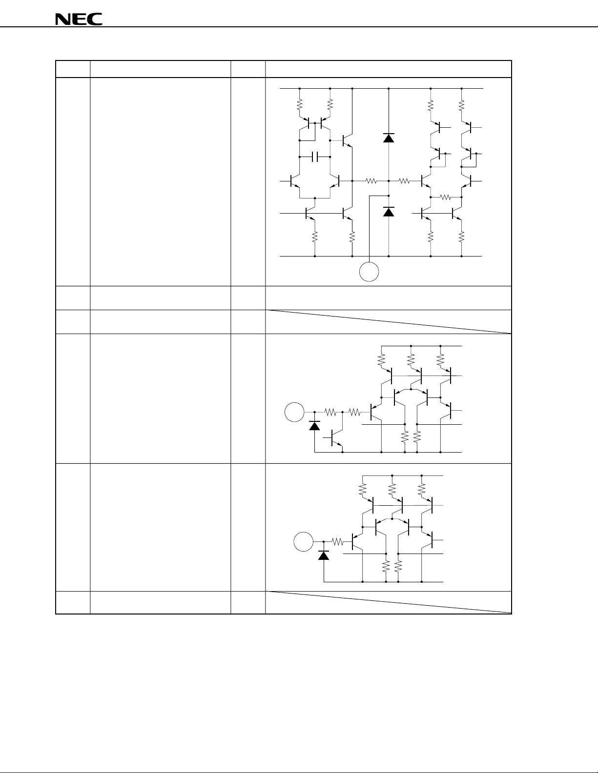
Pin No. Pin Name Symbol Internal Equivalent Circuit
µ
PC1851B
(6/9)
19 Volume Control Offset Absorption VOL-C
10 kΩ10 kΩ
5 pF
20 kΩ
20 VCA Offset Absorption VOA Same as pin 12
21 Analog GND AGND
22 SDA (for I2C bus)
Note
SDA
10 kΩ
5 kΩ
5 kΩ5 kΩ
10 kΩ 10 kΩ
19
10 kΩ 10 kΩ 10 kΩ
25 kΩ
5 kΩ
V
CC
V
CC
GND
23 SCL (for I2C bus)
24 Digital GND (for I2C bus) DGND
Note
SCL
22
50 kΩ5 k
23
5 k
Ω
30 k
10 kΩ 10 kΩ 10 kΩ
Ω
30 k
Ω
30 k
Ω
30 k
Ω
GND
V
CC
Ω
GND
Note A protection diode on the VCC side is deleted not so as to pull the voltage of I2C bus line down to 0 V while
the power supply is off (VCC = 0 V).
14
Data Sheet S13417EJ2V0DS00
Page 15
Pin No. Pin Name Symbol Internal Equivalent Circuit
µ
PC1851B
(7/9)
25 R-channel Output ROT
5 kΩ
26 L-channel Output LOT Same as pin 25
27 Surround Timing SUR
27
10 kΩ
5 kΩ
200 Ω
200Ω
1 kΩ
2 kΩ
1 kΩ
GND
VCC
25
V
CC
28 R-channel Offset Absorption TRO
28
24 kΩ
20 kΩ
20 kΩ40 kΩ
GND
VCC
35 kΩ 5 kΩ
35 kΩ 5 kΩ
40 kΩ
10 kΩ10 kΩ
GND
Data Sheet S13417EJ2V0DS00
15
Page 16
Pin No. Pin Name Symbol Internal Equivalent Circuit
µ
PC1851B
(8/9)
29 R-channel Capacity of High RTC
Frequency Band Width
30 R-channel Capacity of Low RBC
Frequency Band Width
29
30
1 kΩ
5.3 kΩ
3 kΩ
36 kΩ 5 kΩ
36 kΩ 5 kΩ
40 kΩ
10 kΩ 10 kΩ
5 kΩ
5 kΩ
VCC
GND
V
CC
31 L-channel Offset Absorption TLO Same as 28
32 L-channel Capacity of High LTC Same as 29
Frequency Band Width
33 L-channel Capacity of Low LBC Same as 30
Frequency Band Width
34 R-channel Matrix Output MOR Same as 25
35 L-channel Matrix Output MOL
2.5 kΩ
GND
16
Data Sheet S13417EJ2V0DS00
Page 17
Pin No. Pin Name Symbol Internal Equivalent Circuit
36 External R-channel Input 2 ER2
37 External L-channel Input 2 EL2
15 pF
40 kΩ
38 External R-channel Input 1 ER1
36
40 kΩ
µ
PC1851B
10 kΩ10 kΩ
(9/9)
39 External L-channel Input 1 EL1
40 R-channel Fixed Output FOR Same as pin 25
41 L-channel Fixed Output FOL
42 Monaural Offset Absorption MOA Same as pin 18
2
I
C Bus
10 kΩ
Data Sheet S13417EJ2V0DS00
17
Page 18

µ
PC1851B
2. BLOCK FUNCTIONS
2.1 Stereo Demodulation Block
(1) Stereo LPF
This filter eliminates signals in the vicinity of 5 fH to 6 fH, such as SAP (Sub Audio Program) (5 fH) and telemetry
signals (6.5 f
L–R signals by multiplication of the L–R signal with the signal at the L–R carrier frequency (2 fH). The L–R signal
tends to receive interference from the 6 fH signal because a square waveform is used as the switching carrier in this
method. To eliminate this interference, the
adjusted by setting the FILTER SETTING bits (Write register, subaddress 02H, bits D0 to D5).
H) . The
µ
PC1851B’s internal L–R demodulator, which uses a double-balanced circuit, demodulates
µ
PC1851B incorporates traps at 5 fH and 6 fH. The filter response is
(2) Stereo Phase Comparator
The 8 fH signal generated at the Stereo VCO is divided by 8 (4 × 2) and then multiplied by the pilot signal passed
through the stereo LPF. The two signals differ from each other by 90 degrees in terms of phase.
The resistor and capacitor connected to the φD1 and φD2 pins form a filter that smoothes the phase error signal
output from the Stereo Phase Comparator, converting the error signal to the DC voltage. When the voltage difference
φ
between
8 fH.
D1 and φD2 pins becomes 0 V (strictly speaking, not 0 V by the internal offset voltage), the VCO runs at
φ
The lag/lead filter externally connected to the pins
D1 and φD2 determines the capture range.
(3) Stereo VCO
The Stereo VCO runs at 8 fH with the internal capacitor. The frequency is adjusted by setting the STEREO VCO
SETTING bits (Write register, subaddress 01H, bits D0 to D5).
(4) Divider (Flip-flop)
Produces two separate fH signals: the inphase fH signal, and the fH signal differing by 90 degrees from the input
pilot signal by dividing the 8 fH frequency from the Stereo VCO by 8 (4 × 2).
(5) Pilot Discrimination Phase Comparator (Level detector)
Multiplies the pilot signal from the COM pin with the inphase fH signal from the divider. The resulting signal is
smoothed by passing it through the external filter connected to the PD1 and PD2 pins and converted into DC
voltage that is used to determine whether or not a stereo pilot is present (Read register, bit D6).
(6) Pilot Canceler
The fH signal from the divider is added to the stereo signal matrix depending on the level of the input pilot signal
to cancel the pilot signal.
(7) L+R LPF
This LPF which has traps at fH and 24 kHz, allows only the monaural signal to pass through. The filter response
is adjusted by setting the FILTER SETTING bit (Write register, subaddress 02H, bits D0 to D5).
(8) De-emphasis
The 75-µs de-emphasis filter is for the monaural signal. The response is adjusted by setting the FILTER SETTING
bit (Write register, subaddress 02H, bits D0 to D5).
(9) L–R AM Demodulator
Demodulates the L–R AM-DSB modulated signal by multiplying with the 2-fH signal which is synchronized to the
pilot signal. The 2-fH square wave is used as the switching carrier.
18
Data Sheet S13417EJ2V0DS00
Page 19

µ
PC1851B
2.2 SAP Demodulation Block
(1) SAP BPF
Picks up the SAP signal by the 50-kHz and 102-kHz traps and a response peak at 5 fH. The filter response is
adjusted by setting the FILTER SETTING bit (Write register, subaddress 02H, bits D0 to D5).
(2) Noise BPF
The µPC1851B monitors signals picked up by the noise BPF (fO = 180 kHz), and distinguishes noise from
signals. By this method, the µPC1851B prevents faulty SAP detection in a weak electric field. The filter response is
adjusted by setting the FILTER SETTING bit (Write register, subaddress 02H, bits D0 to D5).
.
.
(3) Noise Detector
Performs full-wave rectification of noise from noise BPF, changes it to the DC voltage, and inputs it to the
comparator. When the noise level exceeds the reference level, the Noise detection bit (Read register, bit D4) turns
“1”.
The sensitivity and time constant of the circuit are adjusted by setting the values of the resistor and capacitor
connected to the NDT pin.
(4) SAP Detector
Detects the signal from the SAP BPF and smoothes it through the SDT pin and inputs it to the comparator. When
it detects the SAP signal, the SAP broadcast (Broadcast status) (Read register, bit D5) turns “1”.
(5) SAP Demodulator
The SAP demodulator consists of a phase detector, a loop filter and an SAP VCO (PLL detection circuit).
The SAP VCO oscillates at 10 fH, and performs phase comparison between the signal divided by 2 of the SAP
VCO frequency and the SAP signal to make the PLL. The SAP VCO oscillating frequency is adjusted by setting the
SAP VCO SETTING bit (Write register, subaddress 05H, bits D0 to D5).
(6) SAP LPF
Eliminates the SAP carrier and high-frequency buzz. The filter consists of a 2nd-order LPF and fH trap filter. The
filter response is adjusted by setting the FILTER SETTING bit (Write register, subaddress 02H, bits D0 to D5).
Data Sheet S13417EJ2V0DS00
19
Page 20

µ
PC1851B
2.3 dbx Noise Reduction Block
All the filters required for TV-dbx Noise Reduction are incorporated. These filter responses are adjusted by
setting all the FILTER SETTING bits (Write register, subaddress 02H, bits D0 to D5).
(1) LPF
This LPF has traps at fH and 24 kHz each. The fH trap filter minimizes interference by the fH signal which is not
synchronized with the pilot signal (for example, leakage of the synchronous idle and buzz from the video signal).
(2) 408-Hz LPF
This filter is a de-emphasis filter. Its transfer function is as follows:
1 + j
T(f) =
1 + j
f
5.23k
f
408
(3) Variable Emphasis
It is also called the spectral VCA. It is controlled by the spectral RMS. The transfer function is as follows:
1 + j x
S–1 (f, b) =
1 + j x
f 1 + 51b
20.1k b + 1
f 1 + 51
20.1k b + 1
where “b” is the variable transferred from the spectral RMS for controlling.
(4) Wide-band VCA
A VCA whose operating frequency range is mainly low to mid frequencies and controlled by the wide-band RMS.
The transfer function is as follows:
W–1 (a) = a
where “a” is the variable transferred from the wide-band RMS for controlling.
(5) 2.19-kHz LPF
This filter is a de-emphasis filter. Its transfer function is as follows:
1 + j
T(f) =
1 + j
f
62.5k
f
2.19k
(6) Spectral RMS Filter
A filter that limits the band width of the signal input to the RMS which controls the variable emphasis. The
transfer function is as follows:
ff
( j )
T (f) = x
1 + j
2
7.66k 3.92k
ff f
7.31k 7.66k 3.92k
+ ( j
)21 + j
j
20
Data Sheet S13417EJ2V0DS00
Page 21

µ
PC1851B
(7) Wide-band RMS Filter
A filter that limits the band width of the signal input to the wide-band RMS which controls the wide-band VCA.
The transfer function is as follows:
1 + j
1
f
2.09k
T(f) =
(8) Spectral RMS
Detects the RMS value of the signal passed through the spectral RMS filter, and converts the signal to the DC
voltage. The release time is set by adjusting the current I
capacitor connected to the STI pin. The current IT is adjusted by adjusting the current from the ITI pin.
T of the
µ
PC1851B and the capacitance of the external
(9) Wide-band RMS
Detects the RMS value of the signal passed through the wide-band RMS filter, and converts the signal to the DC
voltage. The release time is set by adjusting the current IT of the µPC1851B and the capacitance of the external
capacitor connected to the WTI pin. The current IT is adjusted by adjusting the current from the ITI pin.
2.4 Matrix Block
(1) Matrix
Adds L+R signal and L–R signal to output L signal, and substracts L+R signal from L–R signal to output R signal.
(2) Mode Selector
The matrix block selects the signal from the monaural signal, Stereo signal, SAP signal by the User Mode.
2.5 Selector Block
It selects the signal from the TV signal (signal with the audio multiple signal processed in the µPC1851B) and
external input (signal input from EL1, EL2, ER1 and ER2 pins), and outputs it to the surround processor block
(surround, tone control, and volume control block).
It also selects the gain of the selection signal (0 dB/6 dB) as well as switches the stereo/monaural output (by the
2
C bus).
I
Data Sheet S13417EJ2V0DS00
21
Page 22

µ
3. I2C BUS INTERFACE
The µPC1851B uses a 2-wire serial bus developed by Philips. The serial clock line (SCL) and serial data line
(SDA) employ the 2-wire configuration as shown in Figure 3-1.
µ
PC1851B contains an I2C bus interface circuit, eleven (8-bit) read/write registers, and one read-only register.
The
Serial Clock Line (SCL)
The master CPU outputs a serial clock to achieve data synchronicity. The µPC1851B receives serial data based
on this clock. The input level is CMOS-compatible. The clock frequency is from 0 to 100 kHz.
Serial Data Line (SDA)
The master CPU outputs data synchronously with the serial clock. The µPC1851B receives this data based on
the serial clock. The input level is CMOS-compatible
Figure 3-1. Internal Equivalent Circuit of Interface Pins
PC1851B
SCL
SDA
For SCL and SDA pins, a protection diode on the V
down to 0 V while the power supply is off (VCC = 0 V).
P
R
PC1851B
µ
CC side is deleted not so as to pull the voltage of I
R
P
2
C bus line
22
Data Sheet S13417EJ2V0DS00
Page 23

µ
PC1851B
3.1 Data Transfer
(1) Start condition
The start condition is created when SDA changes from high to low while SCL is high, as shown in Figure 3-2.
When the µPC1851B receives this information, it captures data sent in synchronization with the clock.
(2) Stop condition
The stop condition is created when SDA changes from low to high while SCL is high, as shown in Figure 3-2.
When the µPC1851B receives this information, it stops receiving or outputting data.
Figure 3-2. Data Transfer Start/Stop Condition
3.5 V
SDA
1.5 V
SCL
Start
4.0 s
µ
MIN.
3.5 V
1.5 V
4.7 s
µ
MIN.
Stop
(3) Data transfer
When transferring data, be sure to switch data only when SCL is low, as shown in Figure 3-3. When SCL is high,
the data must not be changed.
Figure 3-3. Data Transfer
SDA
Note 2Note 1
SCL
Note 3 Note 4
Notes 1. Data hold time: 300 ns MIN.
2. Data setup time: 250 ns MIN.
3. Interval when data must not be changed.
4. Interval when data can be changed.
Data Sheet S13417EJ2V0DS00
23
Page 24

3.2 Data Transfer Format
An example of data transfer in the write mode is shown in Figure 3-4.
Figure 3-4. Data Transfer Example in Write Mode
µ
PC1851B
D6SDA
D5 D4 D3 D2 D1 D0
SCL
123456789 123456789 123456789
Start Slave address Subaddress
Write
mode
Read/
write
Acknowledge
D6 D5D7 D4 D3 D2 D1 D0 D6 D5D7 D4 D3 D2 D1 D0
Acknowledge
Data
Acknowledge
Data consists of 8-bit units. This 8-bit data must always be followed by an acknowledge bit. Data transfer must
be done on an MSB-first basis.
The first byte after a start condition specifies the slave address. The slave address consists of 7 bits.
Table 3-1 shows the slave addresses of the µPC1851B. These slave addresses are registered by Philips.
µ
Table 3-1. Slave Addresses of
PC1851B
Slave address D6 D5 D4 D3 D2 D1 D0 Read/Write
Mode
Stop
Write 1 0 1 1 0 0 0 0
Read 1 0 1 1 0 0 0 1
The bit following the slave address is the read/write bit specifying the direction of the data to be transferred.
During the read operation, data is transferred from the
µ
PC1851B to the master CPU. During the write operation,
data is transferred from the master CPU to the µPC1851B. “0” and “1” are written to the READ/WRITE bit during the
Write and Read modes, respectively.
µ
The byte following the slave address is the subaddress of the
PC1851B in the write mode.
The µPC1851B has eleven subaddresses, SA0 to SAA, which are made up of 8 bits. Following the subaddress
byte is the data to be set to the subaddress.
24
Data Sheet S13417EJ2V0DS00
Page 25

µ
PC1851B
(1) 1-byte data transfer
The format for 1-byte data transfer is the following:
Write
Start
Slave
address
mode
Acknow
-ledge
Subaddress
Acknow
-ledge
Data
Acknow
-ledge
Stop
(2) Continuous data transfer
The format when transferring multiple (7) bytes of data at one time by using the automatic increment function is
the following:
Write
Start
Slave
address
mode
Acknow
-ledge
Subaddress
The master CPU transfers “00H” as subaddress SA0 following the start condition and slave address. After the
subaddress SA0, the master CPU transfers the SA0 data, and continues with SA1, SA2,..., SAA data without transferring
stop conditions in between. Finally, the stop condition is transferred and the transfer is completed.
Acknow
-ledge
Data1
Acknow
-ledge
Data2
Acknow
-ledge
Acknow
-ledge
StopData7
(3) Data read
The µPC1851B has one read register. The contents of this register can be read by the master CPU.
The format when data is read is the following:
Start
Slave
address
Read
Acknow
-ledge
Data
Non-
acknow
-ledge
Stop
(4) Acknowledge
In the case of the I2C bus, an acknowledge bit is added to the data as the 9th bit to determine whether data
transfer was successful. The master CPU determines the success or failure of data transfer based on whether this
acknowledge bit is a logical low or high.
If the acknowledge interval is a logical low, this indicates that data transfer was successful. If it is a logical high,
this indicates that data transfer was unsuccessful or that the slave side forcibly released the bus.
Data Sheet S13417EJ2V0DS00
25
Page 26

µ
PC1851B
(5) Automatic increment
The µPC1851B has the automatic increment function.
The automatic increment is applied to the subaddresses 00H to 05H of the write register.
The user can set ON/OFF the automatic increment of the subaddresses 06H to 0AH (refer to 4.1 Subaddress
List).
Automatic increment ON: The subaddress is automatically increased. Setting the slave address and
subaddress once enables the data of the next subaddress to be transferred
without actually setting it.
Automatic increment OFF: The subaddress is fixed. The data of the fixed subaddress can be set time after
time.
The increment of the subaddresses 06H to 0AH is individually controlled by each automatic increment ON/OFF
bit.
For example, if the automatic increment function of the subaddress 06H is set to ON and that of the subaddress
07H set to OFF, the subaddress is to be automatically increased from 06H to 07H and then fixed to 07H.
Though the automatic increment function of the subaddress 0AH is set to ON, the subaddress is not to be
increased. After setting the data of 0AH (acknowledge bit: low level), if the next data is transferred, the acknowledge
is to be in non-acknowledge state (acknowledge bit: high level) and the data transfer from the master CPU is
aborted.
26
Data Sheet S13417EJ2V0DS00
Page 27

µ
PC1851B
4. I2C BUS COMMANDS
4.1 Subaddress List
(1) Write register (command list)
Bit MSB LSB
Sub- D7 D6 D5 D4 D3 D2 D1 D0
address
00H 0 During noise Input level setting
detection
Stereo/SAP
output stop
0: SAP OFF
1: Stereo,
SAP OFF
01H 0 fH monitor Stereo VCO setting
ON/OFF
0: OFF 1: ON
02H 0 Pilot canceler Filter setting
ON/OFF
0: ON 1: OFF
03H 0 Input gain Low-band separation setting
0: 0 dB 1: 6 dB
04H 0 Surround High-band separation setting
0: OFF 1: ON
05H 0 5fH monitor SAP VCO setting
ON/OFF
0: OFF 1: ON
06H Automatic Input select 1
increment 00: TV signal 0: Stereo switch
0: OFF 01: External input 1 1: Monaural 0: SAP1 0: Stereo 0: OFF 1: OFF
1: ON 10: External input 2 1: SAP2 1: SAP 1: ON
11: Setting prohibited
07H 0 Automatic Volume control
increment
0: OFF 1: ON
08H 0 Automatic Balance control
increment
0: OFF 1: ON
09H 0 Automatic Bass control
increment
0: OFF 1: ON
0AH 0 Automatic Treble control
increment
0: OFF 1: ON
Input select 2
SAP1/SAP2 Stereo/SAP Forced Mute
Note
switch monaural 0: ON
Data Sheet S13417EJ2V0DS00
27
Page 28

Note Output when SAP1 or SAP2 is selectd is as follows:
L-channel output (LOT pin) R-channel output (ROT pin)
SAP1 SAP
SAP2 Monaural (L+R) SAP
(2) Read register
MSB LSB
D7 D6 D5 D4 D3 D2 D1 D0
Broadcast status Reception status
Power-on reset Stereo pilot SAP signal Noise detection Stereo br oadcast SAP broadcast
reception reception 1 1
0: Not available 0: Not available 0: Not available 0: Not available 0: Not available
1: Detect 1: Available 1: Available 1: Available 1: Available 1: Available
µ
PC1851B
28
Data Sheet S13417EJ2V0DS00
Page 29

µ
PC1851B
4.2 Setting Procedure
Precise adjustment of the dbx decoder is absolutely critical for optimum performance. Where possible, the adjustment
should be performed after the µPC1851B is mounted on the chassis and with the video system active.
Set the data of write register as follows before the adjustment.
Table 4-1. Default Setting of Write Register
Bit D7 D6 D5 D4 D3 D2 D1 D0
Subaddress
00H 0 0 1 0 0 0 0 0
01H 0 0 1 0 0 0 0 0
02H 0 0 1 1 1 1 1 1
03H 0 0 1 0 0 0 0 0
04H 0 0 1 0 0 0 0 0
05H 0 0 1 0 0 0 0 0
06H 0 0 0 0 0 0 0 1
07H 0 1 1 1 1 1 1 1
08H 0 1 1 0 0 0 0 0
09H 0 1 1 0 0 0 0 0
0AH 0 1 1 0 0 0 0 0
(1) Input level setting (Write register, subaddress 00H, bits D5 to D0)
<1> Write “1” to bit D0 (Mute: OFF) of subaddress 06H.
<2> Input sine wave of 300 Hz, 150 mVrms to COM pin.
<3> Set bits D5 to D0 (INPUT LEVEL SETTING bits) of subaddress 00H so that the output level of FOR pin is
500 mV
rms (±10 mVrms).
(2) Stereo VCO setting (Write register, subaddress 01H, bits D6 to D0)
Perform this adjustment with no signal applied.
<1> Write “1” to bit D0 (Mute: OFF) of subaddress 06H.
<2> Write “1” to bit D6 (f
<3> Connect frequency counter to FOR pin, and set bits D5 to D0 (STEREO VCO SETTING bits) of subaddress
01H so that frequency counter displays 15.73 kHz (±0.1 kHz).
<4> When setting is completed, write “0” to bit D6 (f
H monitor: ON) of subaddress 01H.
H monitor: OFF) of subaddress 01H.
Data Sheet S13417EJ2V0DS00
29
Page 30

(3) Filter setting (Write register, subaddress 02H, bits D6 to D0)
<1> Write “1” to bit D6 (Pilot canceler: OFF) of subaddress 02H.
<2> Input pilot signal (15.734 kHz, 30 mVrms or higher
SETTING bits) of subaddress 02H so that the AC output level of the FOR pin becomes as small as possible
(Decrease the set data from 63 (decimal)).
<3> When setting is completed, write “0” to bit D6 (pilot canceler: ON) of subaddress 02H.
Note
) to COM pin and set data of bits D5 to D0 (FILTER
µ
PC1851B
Note Recommended 100 mV
rms.
(4) Separation setting (Write register, subaddresses 03H and 04H, bits D5 to D0)
<1> Write “1” to bit D0 (Mute: OFF) of subaddress 06H.
<2> Write “20H” to bits D5 to D0 (HIGH-BAND SEPARATION SETTING bits) of subaddress 04H.
<3> Input composite signal to COM pin (300 Hz, 30 % modulation, L-only, with noise reduction), and set bits D5
to D0 (LOW-BAND SEPARATION SETTING bits) of subaddress 03H so that the output level of the FOR
pin is as small as possible.
<4> Change the modulation frequency of the composite signal to 3 kHz, and set bits D5 to D0 of subaddress
04H so that the output level of the FOR pin is as small as possible.
<5> While bits D5 to D0 of subaddress 04H are set as in step <4> above, repeat the setting procedure of step
<3> for bits D5 to D0 of subaddress 03H.
(5) SAP VCO setting (Write register, subaddress 05H, bits D6 to D0)
Perform this adjustment with no signal applied.
<1> Add a 1 MΩ resistor between the SOA pin and GND.
<2> Write “1” to bit D0 (Mute: OFF) of subaddress 06H.
<3> Write “1” to bit D6 (5 f
<4> Connect a frequency counter to the FOR pin, and set bits D5 to D0 of subaddress 05H (SAP VCO SETTING
bits) so that 78.67 kHz (±0.5 kHz) is displayed on the frequency counter.
<5> When setting is completed, write “0” to bit D6 (5 f
<6> Delete the 1 MΩ resistor between the SOA pin and GND.
H monitor: ON) of subaddress 05H.
H monitor: OFF) of subaddress 05H.
30
Data Sheet S13417EJ2V0DS00
Page 31

µ
PC1851B
4.3 Explanation of Write Register
(1) Stereo/SAP output stop function during noise detection
Stereo/SAP output stop can be selected with the data of bit D6 of subaddress 00H during weak electrical field
conditions (recommended noise level during circuit use is 34 mVrms (TYP.) or more).
SAP output stop : Only SAP output is stopped.
SAP and stereo output stop : SAP and stereo outputs are stopped, switch to monaural output.
Noise level detection is performed, when detected a noise about at 11.5 f
apart from that of the high frequency signals such as the stereo, SAP, and telemetry signal. If noise is detected, “1”
is set to bit D4 of the read register (Refer to section 4.4, (4) Noise detection)
Figure 4-1. Stereo/SAP Output Stop Function During Noise Detection
D7 D6 D5 D4 D3 D2 D1 D0
000H
During noise
detection
Stereo/SAP output stop function during noise detection
0
SAP output stop
1
SAP and stereo output stop
Input level setting
H (180 kHz), a frequency that is sufficiently
(2) Mute
The mute function can be set ON/OFF with the data of bit D0 of subaddress 06H.
The mute on state is entered when bit D0 is set to 0 after power-on reset.
Figure 4-2. Mute
D7 D6 D5 D4 D3 D2 D1 D0
06H
Automatic
increment
Caution When switching the power ON/OFF, use the external mute (200 ms) in order to minimize shock
Input select 1
noise.
Input select 2
SAP1/SAP2
switch
Data Sheet S13417EJ2V0DS00
Stereo/SAP
switch
Forced monaural
ON/OFF
Mute
ON/OFF
Mute
0
Mute ON
1
Mute OFF
31
Page 32

µ
(3) Mode switch (L-, R-channel output (LOT, ROT pins))
The output signal for the L- and R-channel outputs (LOT, ROT pins) can be selected with bits D3 to D1 of
subaddress 06H. For the combinations of data of each output signal bit, refer to 5. MODE MATRIX.
Forced monaural ON/OFF : When set to ON, a monaural signal is forcibly output regardless of the selection
of other bits.
Stereo/SAP switch : When forced monaural is set to OFF, performs selection of stereo or SAP.
SAP1/SAP2 switch : When SAP output is selected with the stereo/SAP switch, performs selection
of SAP1 or SAP2.
L-Channel Output (LOT pin) R-Channel Output (ROT pin)
SAP1 SAP output
SAP2 Monaural (L+R) output SAP output
PC1851B
06H
D7 D6
Automatic
increment
Figure 4-3. Mode Switch (L-, R-Channel Output (LOT, ROT pins))
D5
Input select 1
D4 D3 D2 D1 D0
Input select 2
SAP1/SAP2
switch
Stereo/SAP
switch
Forced monaural
ON/OFF
Mute ON/OFF
Forced monaural
0
Forced monaural OFF
1
Forced monaural ON
Stereo/SAP switch
0
Stereo output
1
SAP output
SAP1/SAP2 switch
0
SAP1 output
1
SAP2 output
32
Data Sheet S13417EJ2V0DS00
Page 33

µ
PC1851B
(4) Input select
The signal to be input to the selector block in the µPC1851B can be selected by the data of bits D4 to D6 of
subaddress 06H. The selected signal is output from the LOT, ROT, FOL and FOR pins.
For the combination of bits for the signal to be selected, refer to 6. SELECTOR TABLE.
µ
Input select 1 : switches the TV signal (signal with the audio multiple signal processed in the
and external inputs 1 and 2 (signal input from EL1, EL2, ER1 and ER2 pins).
Input select 2 : switches the stereo signal and monaural signal.
Figure 4-4. Input Select
PC1851B)
06H
D7
Automatic
increment
D6 D5 D4
Input select 1
Input select 2
D3 D2 D1
SAP1/SAP2
switch
Input select 2
0
Note
1
Input select 1
00
01
10
11
Stereo/SAP
switch
L-channel output
(LOT, FOL pins)
L-channel signal
Monaural (L+R) signal
TV signal
External input 1
External input 2
Setting prohibited
Forced monaural
ON/OFF
R-channel output
(ROT, FOR pins)
R-channel signal
D0
Mute
Note When SAP2 is selected by switching SAP1/SAP2, the L+R signal and SAP signal are composite to be
output.
Data Sheet S13417EJ2V0DS00
33
Page 34

µ
PC1851B
(5) Input gain
The gain of the signal to be input to the selector block in the µPC1851B can be selected by the data of bit D6 of
subaddress 03H.
Figure 4-5. Input Gain
D7 D6 D5 D4 D3 D2 D1 D0
03H
0 Input gain Low-band separation setting
Input gain
0
0 dB
1
6 dB
(6) Surround function
The surround function ON/OFF can be selected by the data of bit D6 of subaddress 04H.
Figure 4-6. Surround Function
04H
D7
0 Surround High-band separation setting
D6 D5 D4 D3 D2 D1 D0
Surround function
34
0
1
Data Sheet S13417EJ2V0DS00
Surround OFF
Surround ON
Page 35

µ
D7
Data
D5 - D0
07H
Volume control
D6 D5 D4 D3 D2 D1 D0
0 Automatic
increment
Volume control
111111
|
000000
Attenuation
volume
Flat (0 dB)
|
Low
D7
08H
D6 D5 D4 D3 D2 D1 D0
0 Automatic
increment
Balance control
Balance control
Data
D5 - D0
111111
|
100000
|
000000
Attenuation
volume
L-ch Low, R-ch Flat
|
TYP.
|
L-ch Flat, R-ch Low
PC1851B
(7) Volume, Balance control
The volume and balance of the output (LOT and ROT pins) can be controlled at 64 levels by the data of bits D0
to D5 of subaddresses 07H and 08H.
The volume attenuation is 80 dB or higher.
Figure 4-7. Volume, Balance Control
• Volume control
• Balance control
Data Sheet S13417EJ2V0DS00
35
Page 36

µ
(8) Bass, Treble control
The bass and treble sound quality of the output (LOT and ROT pins) can be controlled at 64 levels by the data
of the bits D0 to D5 of subaddresses 09H and 0AH.
The bass control amount of the low frequency band width boost/cut is ±11 dB TYP. at 100 Hz.
The treble control amount of the high frequency band width boost/cut is ±13 dB TYP. at 10 kHz.
Figure 4-8. Bass, Treble control
• Bass control
PC1851B
09H
0AH
D7
0 Automatic
• Treble control
D7
0 Automatic
D6 D5 D4 D3 D2 D1 D0
Bass control
increment
Bass control
D5 - D0
111111
100000
000000
D6 D5 D4 D3 D2 D1 D0
Treble control
increment
Data
|
|
Gain
Boost
|
0 dB
|
Cut
36
Data Sheet S13417EJ2V0DS00
Treble control
Data
D5 - D0
111111
|
100000
|
000000
Gain
Boost
|
0 dB
|
Cut
Page 37

µ
PC1851B
(9) Automatic increment function
The automatic increment function ON/OFF can be selected by the data of bit D7 of subaddress 06H and that of
bit D6 of subaddresses 07H to 0AH. For the details of the automatic increment function, refer to 3.2 (5) Automatic
increment.
Figure 4-9. Automatic Increment Function
06H
D7
Automatic
increment
Caution After power-on reset, be sure to set the data.
D6
Input select 1
D5
D4 D3 D2 D1 D0
Input select 2
SAP1/SAP2
switch
Stereo/SAP
switch
Automatic increment function
0
Automatic increment function OFF
1
Automatic increment function ON
Forced monaural
ON/OFF
Mute
Data Sheet S13417EJ2V0DS00
37
Page 38

4.4 Explanation of Read Register
(1) Power-on reset detection
Whether a power-on reset was detected is detected with bit D7 of the read register.
Figure 4-10. Power-On Reset Detection
D7 D6 D5 D4 D3 D2 D1 D0
µ
PC1851B
Power-on
reset
Broadcast status
Stereo
broadcast
Power-on reset detection
1
Power-on reset detection
SAP
broadcast
Noise
detection
Reception status
Stereo
broadcast
reception
SAP
broadcast
reception
11
(2) Stereo, SAP broadcast (broadcast status) detection
Whether SAP or stereo broadcast from a broadcasting station is being broadcast is detected with bits D5 and D6
of the read register.
When a SAP signal (5 f
D7 D6 D5 D4 D3 D2 D1 D0
Power-on
reset
H) or stereo pilot signal is detected, the register data becomes “1”.
Figure 4-11. Stereo, SAP Broadcast (Broadcast Status) Detection
Broadcast status
Stereo
broadcast
SAP
broadcast
Noise
detection
Reception status
Stereo
broadcast
reception
SAP
broadcast
reception
11
38
SAP broadcast
0
No SAP broadcast
1
SAP broadcast (SAP signal detected)
Stereo broadcast
0
No Stereo broadcast
Stereo broadcast (stereo pilot signal detected)
1
Data Sheet S13417EJ2V0DS00
Page 39

µ
0
1
0
1
Stereo broadcast reception
Outputing SAP broadcast
No outputing SAP broadcast
SAP broadcast reception
No outputing stereo broadcast
Outputing stereo broadcast
D7 D6 D5 D4 D3 D2 D1 D0
Power-on
reset
Noise
detection
11
Broadcast status
Stereo
broadcast
SAP
broadcast
Stereo
broadcast
reception
SAP
broadcast
reception
Reception status
PC1851B
(3) Stereo, SAP broadcast reception (reception status) detection
Whether SAP or stereo broadcast is being received and the µPC1851B outputs the audio signal can be detected
with bits D2 and D3 of the read register. The register data become “1” only if the SAP signal (5 fH) is detected when
the SAP broadcast reception is selected, or if the stereo pilot signal is detected when the stereo broadcast reception
is selected.
Figure 4-12. Stereo, SAP Broadcast Reception (Reception Status) Detection
(4) Noise detection
Noise can be detected with bit D4 of the read register. It is monitored in the vicinity of the 11.5 fH (180 kHz) signal
level.
During noise detection, the operation of the SAP demodulator block and the stereo demodulation block is interrupted
(Refer to section 4.3 (1) Stereo/SAP output stop function during noise detection).
Figure 4-13. Noise Detection
D7 D6 D5 D4 D3 D2 D1 D0
Power-on
reset
Broadcast status
Stereo
broadcast
SAP
broadcast
Noise
detection
Reception status
Stereo
broadcast
reception
Noise detection
0
No noise
Noise
1
SAP
broadcast
reception
11
Data Sheet S13417EJ2V0DS00
39
Page 40

µ
PC1851B
5. MODE MATRIX Mute OFF (Write register, subaddress 06H, bit D0 : “1”)
(1) Read register, bit D4: 0
Broadcast Write Register Output Read Register
mode Forced Stereo SAP1 Stereo L-ch R-ch Broadcast status Reception status
monaural /SAP /SAP2 /SAP output output
ON/OFF switch switch output (LOT ) (ROT)
Subaddress
06H 00H
Bit D1 Bit D2 Bit D3 Bit D6 Bit D6 Bit D5 Bit D3 Bit D2
Monaural –––– L+R 0000
Stereo 0–––LR1010
1 L+R 0
Monaural+SAP
Stereo+SAP 00––LR1110
00–– L+R 0100
1 0 SAP 1
1 L+R SAP
1–– L+R 0
10 SAP 01
1 L+R SAP
1–– L+R 0
stop
Subaddress
Stereo SAP Stereo SAP
pilot signal broadcast broadcast
reception reception
(2) Read register, bit D4: 1
Broadcast Write Register Output Read Register
mode Forced Stereo SAP1 Stereo L-ch R-ch Broadcast status Reception status
Monaural –––– L+R 0000
Stereo 0––0LR1010
Monaural+SAP
Stereo+SAP 00–0LR1010
monaural /SAP /SAP2 /SAP outputl output
ON/OFF switch switch output (LOT) (ROT)
Subaddress
06H 00H
Bit D1 Bit D2 Bit D3 Bit D6 Bit D6 Bit D5 Bit D3 Bit D2
0100 L+R 0000
10
100
10
stop
Subaddress
1 L+R 0 0
1
1
1 L+R 0 0
1
1
Stereo SAP Stereo SAP
pilot signal broadcast broadcast
reception reception
Remarks1. When the µPC1851B recognizes a weak electric field, bit D4 of the read register becomes “1”.
2. —: Don’t care.
40
Data Sheet S13417EJ2V0DS00
Page 41

µ
PC1851B
6. SELECTOR TABLE
Input signal:
TV signal (signal with the audio multiple signal processed in the µPC1851B) L-channel, R-channel
External input 1 (signal input from EL1, ER1 pins) L-channel, R-channel
External input 2 (signal input from EL2, ER2 pins) L-channel, R-channel
Write Register Output
Mute ON/OFF Input select 1 Input select 2 L-channel output R-channel output
Subaddress : 06H (LOT, FOL pins) (ROT, FOR pins)
Bit : D0 Bits : D6, D5 Bit : D4
0 – – – Mute
1 00 0 TV signal (L) TV signal (R)
01 External input 1 (L) External input 1 (R)
10 External input 2 (L) External input 2 (R)
11 Setting prohibited (no signal, unconnected)
00 1 TV signal (L+R)
01 External input 1 (L+R)
10 External input 2 (L+R)
11 Setting prohibited (no signal, unconnected)
1
2
1
2
1
2
Remark – : Don’t care
Data Sheet S13417EJ2V0DS00
41
Page 42

µ
7. USAGE CAUTIONS
7.1 Caution on Shock Noise Reduction
When switching the power ON/OFF, use the external mute (approx. 200 ms) in order to minimize shock noise
(Refer to section 4.3 (2) Mute).
7.2 Supply Voltage
Pass data through the I2C bus only after stabilizing the supply voltage of the entire application system.
7.3 Impedance of Input and Output Pins
Table 7-1. Impedance of Input and Output Pins
Input pin Output pin
PC1851B
Symbol Description Impedance Symbol Description Impedance
COM Composite signal input 80 kΩ SOT SAP single input 360 Ω
SI SAP single input ROT R-channel output 15 Ω
EL1, EL2 External L-channel input LOT L-channel output
ER1, ER2 External R-channel input MOR R-channel matrix output
MOL L-channel matrix output
FOR R-channel fixed output
FOL L-channel fixed output
7.4 Drive Capability of Output Pins
Table 7-2. Drive Capability of Output Pins
Pin symbol Pin description Output pin-GND Connection Resistance Drive capability
SOT SAP single output 10 kΩ 3-kΩ load or less
ROT R-channel output 700-Ω load or less
LOT L-channel output
MOR R-channel matrix output
MOL L-channel matrix output
FOR R-channel fixed output
FOL L-channel fixed output
Remark If the load capacitance of the output pins (SOT, ROT, LOT, MOR, MOL, FOR, FOL pins) exceeds
100 pF, parasitic oscillation may occur. In this case, connect a resistor between the output pins
and the load capacitance. Bear in mind that the load capacitance is changed by wiring pattern on
the printed circuit board.
42
Data Sheet S13417EJ2V0DS00
Page 43

7.5 Caution on External Components
According to the license contract with THAT Corporation, use the following for external components.
With regard to the use of other external components, please contact to THAT corporation.
Table 7-3. External Components
Pin symbol Pin description External component
ITI Timing current setting Metal film resistor (± 1 %)
STI Spectral RMS timing Tantalum capacitor (±10 %)
WTI Wide-band RMS timing
7.6 Change of Electrical Characteristics by External Components
(1) SAP sensitivity can be lowered by inserting a resistor between the SDT pin and GND.
µ
PC1851B
(2) Noise sensitivity can be changed by changing the value of the resistor between the NDT pin and GND.
µ
(3) The capture range can be changed by changing the recommended 1
φ
D1 and φD2 pins.
Reducing the capacitor value increases the capture range, and increasing it reduces the capture range.
However, too small a capacitor value may cause the distortion rate to become worse during stereo output,
or may cause malfunction. In this case, please contact NEC.
F value of the capacitor between the
Data Sheet S13417EJ2V0DS00
43
Page 44

µ
PC1851B
8. ELECTRICAL SPECIFICATIONS Absolute Maximum Ratings (unless otherwise specified, TA = 25 °C)
Parameter Symbol Conditions Ratings Unit
Power supply voltage VCC VCC pin 11.0 V
I2C bus input pin voltage Vcont SDA, SCL pins VCC V
Composite signal input voltage Vin COM pin VCC V
Package power dissipation PD 700 mW
Operating ambient temperature TA VCC = 9 V –20 to +75 °C
Storage temperature Tstg –40 to +125 °C
Caution Exposure to Absolute Maximum Rating for extended periods may affect device reliability;
exceeding the ratings could cause permanent damage. The parameters apply independently.
Recommended Operating Conditions (unless otherwise specified, TA = 25 ˚C)
Parameter Symbol Conditions MIN. TYP. MAX. Unit
Power supply voltage VCC VCC pin 8.0 9.0 10.0 V
I2C bus input pin voltage (High level)
I2C bus input pin voltage (Low level)
Input impedance Rin COM, SI, EL1, EL2, ER1, ER2 pins 60 – 95 kΩ
Output load impedance 1 RL1 LOT, ROT, MOL, MOR, FOL, FOR pins, 2.0 – – kΩ
Output load impedance 2 RL2 SOT pin, AC load impedance at 100 % 10.0 – – kΩ
Output load impedance 3 RL3 LOT, ROT, MOL, MOR, FOL, FOR pins, 5.0 – – kΩ
Output load impedance 4 RL4 SOT pin, DC load impedance at 100 % 25.0 – – kΩ
Composite signal input voltage Vin COM pin L+R signal, 100 % modulation – 0.424 – Vp-p
External input signal voltage Vext EL1, EL2, ER1, ER2 pins – 1.4 5.6 Vp-p
Clock frequency fSCL SCL pin – – 100 kHz
Vcont(H) SDA, SCL pins 3.5 – 5.0 V
Vcont(L) 0 – 1.5 V
AC load impedance at 100 % modulation
modulation
DC load impedance at 100 % modulation
modulation
L–R signal, 100 % modulation – 0.848 – Vp-p
Pilot signal – 0.0848 – Vp-p
SAP signal – 0.254 – Vp-p
44
Data Sheet S13417EJ2V0DS00
Page 45

µ
PC1851B
Electrical Characteristics
(unless otherwise specified, TA = 25 °C, RH ≤ 70 %, VCC = 9.0 V, adding 30 kHz LPF to output pins)
(1/3)
Parameter Symbol Conditions MIN. TYP. MAX. Unit
Input: COM pin, Output: FOL, FOR pins
Supply current ICC No signal – 57 75 mA
Stereo detection input sensitivity STSENCE 15.734 kHz, sine wave 11 16 21 mVrms
Stereo detection hysteresis STHY Only stereo pilot signal input 5.0 5.7 10 dB
Stereo detection capture range STCCL Vin = 30 mVrms –5.5 –4.0 –2.5 %
STCCH Only stereo pilot signal input +2.5 +4.0 +5.5 %
SAP detection input sensitivity SAPSENCE f = 78.67 kHz, 0% modulation 17 23 30 mVrms
SAP detection hysteresis SAPHY Only SAP carrier input 3.3 4.8 6.3 dB
Noise detection input sensitivity NOSENCE Input sine wave 20 30 40 mVrms
f: Noise BPF peak
Noise detection hysteresis NOHY Input sine wave 1 2 3 dB
f: Noise BPF peak
Monaural total output voltage VOMO 300 Hz, 100% modulation, 480 500 520 mVrm
Pre-emphasis: ON
Stereo total output voltage VOST 300 Hz, 100 % modulation 450 500 550 mVrms
SAP total output voltage VOSAP1 Noise reduction: ON 400 500 600 mVrms
Difference between monaural L and R VOLR 300 Hz, 100% modulation –0.5 – +0.5 dB
output voltage
Monaural total frequency characteristics 1 VOMO1 1 kHz, 30% modulation, (f = 300 Hz: 0 dB) –0.5 – +0.5 dB
Pre-emphasis: ON
Monaural total frequency characteristics 2 VOMO2 3 kHz, 30% modulation, (f = 300 Hz: 0 dB) –0.5 – +0.5 dB
Pre-emphasis: ON
Monaural total frequency characteristics 3 VOMO3 8 kHz, 30% modulation, (f = 300 Hz: 0 dB) –0.8 – +0.8 dB
Pre-emphasis: ON
Monaural total frequency characteristics 4 VOMO4 12 kHz, 30% modulation, (f = 300 Hz: 0 dB) –5.5 –3.0 –1.5 dB
Pre-emphasis: ON
Stereo total frequency characteristics 1 VOST1 1 kHz, 30% modulation, (f = 300 Hz: 0 dB) –0.5 – +0.5 dB
Noise reduction: ON
Stereo total frequency characteristics 2 VOST2 3 kHz, 30% modulation, (f = 300 Hz: 0 dB) –0.5 – +0.5 dB
Noise reduction: ON
Stereo total frequency characteristics 3 VOST3 8 kHz, 30% modulation, (f = 300 Hz: 0 dB) –1.0 – +1.0 dB
Noise reduction: ON
Stereo total frequency characteristics 4 VOST4 12 kHz, 30% modulation, (f = 300 Hz: 0 dB) –8.0 –5.0 –2.0 dB
Noise reduction: ON
SAP total frequency characteristics 1 VOSAP11 1 kHz, 30% modulation, (f = 300 Hz: 0 dB) –1.2 +0.3 +1.2 dB
Noise reduction: ON
SAP total frequency characteristics 2 VOSAP12 3 kHz, 30% modulation, (f = 300 Hz: 0 dB) –1.2 0.0 +1.2 dB
Noise reduction: ON
SAP total frequency characteristics 3 VOSAP13 8 kHz, 30% modulation, (f = 300 Hz: 0 dB) –4.0 –1.0 +1.0 dB
Noise reduction: ON
Stereo channel separation 1 Sep1 300 Hz, 30% modulation 27 32 – dB
Data Sheet S13417EJ2V0DS00
45
Page 46

µ
PC1851B
Parameter Symbol Conditions MIN. TYP. MAX. Unit
Stereo channel separation 2 Sep2 1 kHz, 30% modulation 23 30 – dB
Stereo channel separation 3 Sep3 3 kHz, 30% modulation 27 35 – dB
Stereo channel separation 4 Sep4 5 kHz, 30 % modulation 23 30 – dB
Stereo channel separation 5 Sep5 8 kHz, 30 % modulation – 25 – dB
Monaural total harmonic distortion THDMO 1 kHz, 100% modulation – 0.1 0.5 %
Pre-emphasis: ON
Stereo total harmonic distortion 1 THDST1 1 kHz, 100% modulation – 0.3 1.5 %
Noise reduction: ON
Stereo total harmonic distortion 2 THDST2 8 kHz, 30% modulation – 0.8 1.8 %
Noise reduction: ON
SAP total harmonic distortion THDSAP 1 kHz, 100% modulation – 0.5 2.0 %
Noise reduction: ON
Crosstalk 1 (SAP → Stereo) CT1 SAP : 1 kHz, 100 % modulation – – –65 dB
Stereo : Pilot signal only, 0 % modulation
Filter: 1 kHz BPF
User mode: Stereo
Crosstalk 2 (Stereo → SAP) CT2 Stereo : 1 kHz, 100 % modulation, – – –65 dB
SAP : Carrier only, 0 % modulation
Filter: 1 kHz BPF
User mode: SAP1
Monaural total S/N S/NMO 300 Hz, 100% modulation 65 68 – dB
Pre-emphasis: ON
Stereo total S/N S/NST 300 Hz, 100 % modulation 60 65 – dB
SAP total S/N S/NSAP Noise reduction: ON 70 80 – dB
Input: External input pins, output: LOT, ROT pins
Total muting level
Timing current IT Current provided to STI and WTI pins 7.1 7.5 7.9
Inter-mode DC offset 1 VDOF1 Mute → Monaural –50 – +50 mV
Inter-mode DC offset 2 VDOF2 Mute → Stereo –50 – +50 mV
Inter-mode DC offset 3 VDOF3 Mute → SAP1 –50 – +50 mV
Inter-mode DC offset 4 VDOF4 Mute → External input –50 – +50 mV
Surround output characteristics 1 VSR1L External L-channel input : 100 Hz, 150 mVrms –7.5 –4.5 0.0 dB
Surround output characteristics 2 VSR2L External L-channel input : 1 kHz, 150 mVrms 4.0 5.6 7.0 dB
Surround output characteristics 3 VSR3L External L-channel input : 10 kHz, 150 mVrms 4.5 – 8.0 dB
Surround output characteristics 4 VSR4R External L-channel input : 1 kHz, 150 mVrms –1.5 – +1.5 dB
Mute TV signal : 1 kHz, 100 % modulation
External input : 1 kHz, 500 mVrms
Surround : ON, LOT pin
Surround : ON, LOT pin
Surround : ON, LOT pin
Surround : ON, ROT pin
80 – – dB
µ
(2/3)
A
46
Data Sheet S13417EJ2V0DS00
Page 47

µ
PC1851B
(3/3)
Parameter Symbol Conditions Sub- Data MIN. TYP. MAX. Unit
address
Low frequency band width boost control VBB 100 Hz, 09H 3FH 9 11 13 dB
Low frequency band width cut control VBC External input = 150 mVrms 00H –13 –11 –9 dB
High frequency band width boost control VTB 10 kHz, 0AH 3FH 10 13 16 dB
High frequency band width cut control VTC External input = 150 mVrms 00H –16 –13 –10 dB
Volume attenuation 1 ATTVL1 1 kHz, 07H 3FH –1.0 0.0 +1.0 dB
Volume attenuation 2 ATTVL2 External input = 500 mVrms 20H –20 –17.5 –14 dB
Volume attenuation 3 ATTVL3 00H – – –80 dB
Balance attenuation L-ch 1 ATTBL1 1 kHz, 08H 3FH – – –60 dB
Balance attenuation L-ch 2 ATTBL2 External input = 500 mVrms 30H –14 –10 –6 dB
Balance attenuation L-ch 3 ATTBL3 20H –1.0 0.0 +1.0 dB
Balance attenuation L-ch 4 ATTBL4 00H –1.0 0.0 +1.0 dB
Balance attenuation R-ch 1 ATTBR1 3FH –1.0 0.0 +1.0 dB
Balance attenuation R-ch 2 ATTBR2 20H –1.0 0.0 +1.0 dB
Balance attenuation R-ch 3 ATTBR3 10H –14 –10 –6 dB
Balance attenuation R-ch 4 ATTBR4 00H – – –60 dB
Difference between monaural L and R VOLR1 1 kHz, 07H 3FH –1.5 0.0 +1.5 dB
output voltage 1 External input = 500 mVrms
(in case of external input)
Difference between monaural L and R VOLR2 20H –2.0 0.0 +2.0 dB
output voltage 2
(in case of external input)
Difference between monaural L and R VOLR3 10H –3.0 0.0 +3.0 dB
output voltage 3
(in case of external input)
Crosstalk 3 CT3 TV signal: 1 kHz, 07H 3FH – – –80 dB
TV signal → External input 100 % modulation
Crosstalk 4 CT4 External input: – –80 –70 dB
L-ch → R-ch 1 kHz, 500 mVrms
Total harmonic distortion THDEXT 1 kHz, 07H 3FH – 0.1 0.5 %
(in case of external input) External input = 500 mVrms
Maximum input voltage of external input VIEM 1 kHz, 07H 3FH 1.7 2.1 – Vrms
Total harmonic
distortion rate: 1 %
(External input)
Output noise NO No signal, Rg = 600 Ω, 07H 3FH – 50 150µVrms
(in case of external input) Filter: DIN/AUDIO
Data Sheet S13417EJ2V0DS00
47
Page 48

µ
PC1851B
Test Condition Parameters for Electrical Characteristics
(Unless otherwise specified, TA = 25 ˚C, RH ≤ 70 %, VCC = 9 V, adding 30 kHz LPF to output pins)
(1/8)
Parameter Symbol Test Conditions
Supply current ICC ICC : Current sent to VCC pin when there is no signal Monaural
Stereo detection input STSENCE STSENCE : Input signal level of COM pin (input signal: 15.734 kHz) Stereo
sensitivity When read register D6 changes from 0 to 1
Stereo detection hysteresis STHY STHY =20 log (STSENCE ÷ V)
STSENCE: Stereo detection input sensitivity
V: Input signal level of COM pin (Input signal: 15.734 kHz)
Read register D6 is first set to 1, then input signal level is gradually
lowered until D6 is changed to 0
Stereo detection STCCL STCCL = ∆f ÷ 15.734 kHz
capture range ∆f: Difference between f and 15.734 kHz
f: Input signal (14.5 kHz, 30 mVrms) to COM pin.
Gradually raise frequency and measure frequency
when read register D6 becomes 1.
STCCH STCCH = ∆f ÷ 15.734 kHz
∆f: Difference between f and 15.734 kHz
f: Input signal (17.0 kHz, 30 mVrms) to COM pin.
Gradually lower frequency and measure frequency
when read register D6 becomes 1.
SAP detection input SAPSENCE SAPSENCE : Input signal level of COM pin (input signal: 78.67 kHz) SAP
sensitivity When read register D5 changes from 0 to 1
SAP detection hysteresis SAPHY SAPHY =20 log (SAPSENCE ÷ V)
SAPSENCE: SAP detection input sensitivity
V: Input signal level of COM pin (Input signal: 78.67 kHz)
When read register D5 is first set to 1, input signal level is gradually
lowered until D5 becomes 0.
Noise detection input NOSENCE NOSENCE: Input signal level of COM pin SAP
sensitivity Read register D4: Apply 6-V DC voltage to SDT pin to change it to 0
Read register D4: Input signal (160 kHz, 10 mVrms) to COM pin.
Raise the frequency until the DC voltage of the NDT pin reaches
the maximum level, and then, while maintaining the frequency
level, gradually raise the input signal level until D4 becomes 1.
Noise detection hysteresis NOHY NOHY = 20 log (NOSENCE ÷ V)
NOSENCE: Noise detection input sensitivity
V: Input signal level of NDT pin
COM pin: Signal (160 kHz, 10 mVrms) input
After read register D4 is set to 1, raise the frequency until the DC
voltage of the NDT pin reaches the maximum level, and then,
while maintaining the frequency level, gradually lower the input
signal level until D4 becomes 0.
Monaural total output voltage
Stereo total output voltage VOST L-channel Stereo
VOMO VOMO : Output voltage of FOL and FOR pins Monaural
COM pin: Monaural signal (300 Hz, 100 % modulation) input
VOST : Output voltage of FOL pin
COM pin: Stereo signal (L-only, 300 Hz, 100 % modulation) input
R-channel
VOST : Output voltage of FOR pin
COM pin: Stereo signal (R-only, 300 Hz, 100 % modulation) input
User Mode
Note
Note For details about the User Mode, refer to 5. MODE MATRIX.
48
Data Sheet S13417EJ2V0DS00
Page 49

µ
PC1851B
Parameter Symbol Test Conditions
SAP total output voltage VOSAP1 VOSAP1 : Output voltage of FOL and FOR pins SAP1
COM pin: SAP signal (300 Hz, 100 % modulation) input
Difference between monaural
L and R output voltage
Monaural total frequency VOMO1 VOMO1 = 20 log {V(1k) ÷ V(300)} Monaural
characteristics 1 V(1k): Output voltage of FOL pin
Monaural total frequency VOMO2 VOMO2 = 20 log {V(3k) ÷ V(300)}
characteristics 2 V(3k): Output voltage of FOL pin
Monaural total frequency VOMO3 VOMO3 = 20 log {V(8k) ÷ V(300)}
characteristics 3 V(8k): Output voltage of FOL pin
Monaural total frequency VOMO4 VOMO4 = 20 log {V(12k) ÷ V(300)}
characteristics 4 V(12k): Output voltage of FOL pin
Stereo total frequency VOST1 VOST1 = 20 log {V(1k) ÷ V(300)} Stereo
characteristics 1 V(1k): Output voltage of FOL pin
Stereo total frequency VOST2 VOST2 = 20 log {V(3k) ÷ V(300)}
characteristics 2 V(3k): Output voltage of FOL pin
Stereo total frequency VOST3 VOST3 = 20 log {V(8k) ÷ V(300)}
characteristics 3 V(8k): Output voltage of FOL pin
Stereo total frequency VOST4 VOST4 = 20 log {V(12k) ÷ V(300)}
characteristics 4 V(12k): Output voltage of FOL pin
VOLR VOLR = 20 log (VL ÷ VR) Monaural
VL: Output voltage of FOL pin
COM pin: Monaural signal (300 Hz, 100 % modulation) input
VR: Output voltage of FOR pin
COM pin: Monaural signal (300 Hz, 100 % modulation) input
COM pin: Monaural signal (1 kHz, 30 % modulation) input
V(300): Output voltage of FOL pin
COM pin: Monaural signal (300 Hz, 30 % modulation) input
COM pin: Monaural signal (3 kHz, 30 % modulation) input
V(300): Output voltage of FOL pin
COM pin: Monaural signal (300 Hz, 30 % modulation) input
COM pin: Monaural signal (8 kHz, 30 % modulation) input
V(300): Output voltage of FOL pin
COM pin: Monaural signal (300 Hz, 30 % modulation) input
COM pin: Monaural signal (12 kHz, 30 % modulation) input
V(300): Output voltage of FOL pin
COM pin: Monaural signal (300 Hz, 30 % modulation) input
COM pin: Stereo signal (L-only, 1 kHz, 30 % modulation) input
V(300): Output voltage of FOL pin
COM pin: Stereo signal (L-only, 300 Hz, 30 % modulation) input
COM pin: Stereo signal (L-only, 3 kHz, 30 % modulation) input
V(300): Output voltage of FOL pin
COM pin: Stereo signal (L-only, 300 Hz, 30 % modulation) input
COM pin: Stereo signal (L-only, 8 kHz, 30 % modulation) input
V(300): Output voltage of FOL pin
COM pin: Stereo signal (L-only, 300 Hz, 30 % modulation) input
COM pin: Stereo signal (L-only, 12 kHz, 30 % modulation) input
V(300): Output voltage of FOL pin
COM pin: Stereo signal (L-only, 300 Hz, 30 % modulation) input
User Mode
(2/8)
Note
Note For details about the User Mode, refer to 5. MODE MATRIX.
Data Sheet S13417EJ2V0DS00
49
Page 50

µ
PC1851B
Parameter Symbol Test Conditions
SAP total frequency VOSAP11 VOSAP11 = 20 log {V(1k) ÷ V(300)} SAP1
characteristics 1 V(1k): Output voltage of FOL pin
COM pin: SAP signal (1 kHz, 30 % modulation) input
V(300): Output voltage of FOL pin
COM pin: SAP signal (300 Hz, 30 % modulation) input
SAP total frequency VOSAP12 VOSAP12 = 20 log {V(3k) ÷ V(300)}
characteristics 2 V(3k): Output voltage of FOL pin
COM pin: SAP signal (3 kHz, 30 % modulation) input
V(300): Output voltage of FOL pin
COM pin: SAP signal (300 Hz, 30 % modulation) input
SAP total frequency VOSAP13 VOSAP13 = 20 log {V(8k) ÷ V(300)}
characteristics 3 V(8k): Output voltage of FOL pin
COM pin: SAP signal (8 kHz, 30 % modulation) input
V(300): Output voltage of FOL pin
COM pin: SAP signal (300 Hz, 30 % modulation) input
Stereo channel Sep1 L-channel Stereo
separation 1 Sep1 = 20 log (VL ÷ VR)
VL: Output voltage of FOL pin
COM pin: Stereo signal (L-only, 300 Hz, 30% modulation) input
VR: Output voltage of FOR pin
COM pin: Stereo signal (L-only, 300 Hz, 30 % modulation) input
R-channel
Sep1 = 20 log (VR ÷ VL)
VR: Output voltage of FOR pin
COM pin: Stereo signal (R-only, 300 Hz, 30 % modulation) input
VL: Output voltage of FOL pin
COM pin: Stereo signal (R-only, 300 Hz, 30 % modulation) input
Stereo channel Sep2 L-channel
separation 2 Sep2 = 20 log (VL ÷ VR)
VL: Output voltage of FOL pin
COM pin: Stereo signal (L-only, 1 kHz, 30 % modulation) input
VR: Output voltage of FOR pin
COM pin: Stereo signal (L-only, 1 kHz, 30 % modulation) input
R-channel
Sep2 = 20 log (VR ÷ VL)
VR: Output voltage of FOR pin
COM pin: Stereo signal (R-only, 1 kHz, 30 % modulation) input
VL: Output voltage of FOL pin
COM pin: Stereo signal (R-only, 1 kHz, 30 % modulation) input
Stereo channel Sep3 L-channel
separation 3 Sep3 = 20 log (VL ÷ VR)
VL: Output voltage of FOL pin
COM pin: Stereo signal (L-only, 3 kHz, 30 % modulation) input
VR: Output voltage of FOR pin
COM pin: Stereo signal (L-only, 3 kHz, 30 % modulation) input
R-channel
Sep3 = 20 log (VR ÷ VL)
VR: Output voltage of FOR pin
COM pin: Stereo signal (R-only, 3 kHz, 30 % modulation) input
VL: Output voltage of FOL pin
COM pin: Stereo signal (R-only, 3 kHz, 30 % modulation) input
User Mode
(3/8)
Note
Note For details about the User Mode, refer to 5. MODE MATRIX.
50
Data Sheet S13417EJ2V0DS00
Page 51

µ
PC1851B
Parameter Symbol Test Conditions
Stereo channel separation 4
Stereo channel separation 5
Monaural total harmonic THDMO THD MO : Distortion rate of FOL and FOR pins Monaural
distortion COM pin: Monaural signal (1 kHz, 100 % modulation) input
Stereo total harmonic THDST1 L-channel Stereo
distortion 1 THDST1 : Distortion rate of FOL pin
Stereo total harmonic THDST2 L-channel
distortion 2 THDST2 : Distortion rate of FOL pin
SAP total harmonic THDSAP THDSAP : Distortion rate of FOL and FOR pins SAP1
distortion COM pin: SAP signal (1 kHz, 100 % modulation) input
Crosstalk 1 (SAP→Stereo) CT1 CT1 = 20 log (VCT1 ÷ 500 mV) Stereo
Crosstalk 2 (Stereo→SAP) CT2 CT2 = 20 log (VCT2 ÷ 500 mV) SAP1
Sep4 L-channel Stereo
Sep4 = 20 log (VL ÷ VR)
VL: Output voltage of FOL pin
COM pin: Stereo signal (L-only, 5 kHz, 30 % modulation) input
VR: Output voltage of FOR pin
COM pin: Stereo signal (L-only, 5 kHz, 30 % modulation) input
R-channel
Sep4 = 20 log (VR ÷ VL)
VR: Output voltage of FOR pin
COM pin: Stereo signal (R-only, 5 kHz, 30 % modulation) input
VL: Output voltage of FOL pin
COM pin: Stereo signal (R-only, 5 kHz, 30 % modulation) input
Sep5 L-channel
Sep5 = 20 log (VL ÷ VR)
VL: Output voltage of FOL pin
COM pin: Stereo signal (L-only, 8 kHz, 30 % modulation) input
VR: Output voltage of FOR pin
COM pin: Stereo signal (L-only, 8 kHz, 30 % modulation) input
R-channel
Sep5 = 20 log (VR ÷ VL)
VR: Output voltage of FOR pin
COM pin: Stereo signal (R-only, 8 kHz, 30 % modulation) input
VL: Output voltage of FOL pin
COM pin: Stereo signal (R-only, 8 kHz, 30 % modulation) input
COM pin: Stereo signal (L-only, 1 kHz, 100 % modulation) input
R-channel
THDST1 : Distortion rate of FOR pin
COM pin: Stereo signal (R-only, 1 kHz, 100 % modulation) input
COM pin: Stereo signal (L-only, 8 kHz, 30 % modulation) input
R-channel
THDST2 : Distortion rate of FOR pin
COM pin: Stereo signal (R-only, 8 kHz, 30 % modulation) input
VCT1: Measure output voltage of FOL or FOR pins after BPF (1 kHz)
SAP: 1 kHz, 100 % modulation
Stereo: Pilot signal only, 0 % modulation
VCT2: Measure output voltage of FOL or FOR pins after BPF (1 kHz)
Stereo: 1 kHz, 100 % modulation
SAP: Carrier only, 0 % modulation
User Mode
(4/8)
Note
Note For details about the User Mode, refer to 5. MODE MATRIX.
Data Sheet S13417EJ2V0DS00
51
Page 52

µ
PC1851B
Parameter Symbol Test Conditions
Monaural total S/N S/NMO L-channel Monaural
S/NMO = 20 log (VOMOL ÷ VL)
VOMOL : Output voltage of FOL pin after LPF (30 kHz)
COM pin: Monaural signal (300 Hz, 100 % modulation) input
VL: Output voltage of FOL pin (no signal)
R-channel
S/NMO = 20 log (VOMOR ÷ VR)
VOMOR: Output voltage of FOR pin after LPF (30 kHz)
COM pin: Monaural signal (300 Hz, 100 % modulation) input
VR: Output voltage of FOR pin (no signal)
Stereo total S/N S/NST L-channel Stereo
S/NST = 20 log (VOSTL ÷ VL)
VOSTL : Output voltage of FOL pin after LPF (30 kHz)
COM pin: Stereo signal (L-only, 300 Hz, 100 % modulation) input
VL: Output voltage of FOL pin
COM pin: Pilot signal input
R-channel
S/NST = 20 log (VOSTR ÷ VR)
VOSTR : Output voltage of FOR pin after LPF (30 kHz)
COM pin: Stereo signal (R-only, 300 Hz, 100 % modulation) input
VR: Output voltage of FOR pin
COM pin: Pilot signal input
SAP total S/N S/NSAP L-channel SAP1
S/NSAP = 20 log (VOSAP1L ÷ VL)
VOSAP1L : Output voltage of FOL pin after LPF (30 kHz)
COM pin: SAP signal (300 Hz, 100 % modulation) input
VL: Output voltage of FOL pin
COM pin: SAP carrier (0 % modulation) input
R-channel
S/NSAP = 20 log (VOSAP1R ÷ VR)
VOSAP1R : Output voltage of FOR pin after LPF (30 kHz)
COM pin: SAP signal (300 Hz, 100 % modulation) input
VR: Output voltage of FOR pin
COM pin: SAP carrier (0 % modulation) input
Total muting level Mute Mute = 20 log (VOMOL ÷ VM) Monaural
VOMOL : Output voltage of LOT pin mute
COM pin: Monaural signal (1 kHz, 100 % modulation) input
VM : Output voltage of LOT pin
Write register 06H, D0: 0
COM pin: Monaural signal (1 kHz, 100 % modulation) input
Timing current IT IT : Current that flows from VCC to STI, WTI pins
STI, WTI pins : 6 V DC is applied.
Inter-mode DC offset 1 V DOF1 VDOF1 = VMONO – VMute Mute
VMONO : DC voltage at LOT and ROT pins to
User mode : Monaural Monaural
NDT pin: 6 V DC is applied.
VMute : DC voltage at LOT and ROT pins
User mode : Mute (write register 06H, D1: 0)
NDT pin: 6 V DC is applied.
User Mode
(5/8)
Note
Note For details about the User Mode, refer to 5. MODE MATRIX.
52
Data Sheet S13417EJ2V0DS00
Page 53

µ
PC1851B
Parameter Symbol Test Conditions
Inter-mode DC offset 2 VDOF2 VDOF2 = VST – VMute Mute
VST : DC voltage at LOT and ROT pins to
User mode : Stereo Stereo
NDT pin: 6 V DC is applied.
VMute : DC voltage at LOT and ROT pins
User mode : Mute (write register 06H, D1: 0)
NDT pin: 6 V DC is applied.
Inter-mode DC offset 3 VDOF3 VDOF3 = VSAP – VMute Mute
VSAP : DC voltage at LOT and ROT pins to
User mode : SAP1 SAP1
NDT pin: 6 V DC is applied.
VMute : DC voltage at LOT and ROT pins
User mode : Mute (write register 06H, D1: 0)
NDT pin: 6 V DC is applied.
Inter-mode DC offset 4 VDOF4 VDOF4 = VMONO – VMute Mute
VMONO : DC voltage at LOT and ROT pins to
User mode : External input External
NDT pin: 6 V DC is applied. input
VMute : DC voltage at LOT and ROT pins
User mode : Mute (write register 06H, D1: 0)
NDT pin: 6 V DC is applied.
Surround output VSR1L VSR1L = 20 log (VL1 ÷ VEL)
characteristics 1 VL1: Output voltage of LOT pin
VEL: Input voltage of EL1, EL2 pins (100 Hz, 150 mVrms)
ER1, ER2 pins: No signal
Surround: ON (Subaddress 04H, Bit D6: 1)
Surround output VSR2L VSR2L : 20 log (VL2 ÷ VEL)
characteristics 2 VL2: Output voltage of LOT pin
VEL: Input voltage of EL1, EL2 pins (1 kHz, 150 mVrms)
ER1, ER2 pins: No signal
Surround: ON (Subaddress 04H, Bit D6: 1)
Surround output VSR3L V SR3L : 20 log (VL3 ÷ VEL)
characteristics 3 VL3: Output voltage of LOT pin
VEL: Input voltage of EL1, EL2 pins (10 kHz, 150 mVrms)
ER1, ER2 pins: No signal
Surround: ON (Subaddress 04H, Bit D6: 1)
Surround output VSR4R VSR4R : 20 log (VR ÷ VEL)
characteristics 4 VR: Output voltage of ROT pin
VEL: Input voltage of EL1, EL2 pins (1 kHz, 150 mVrms)
ER1, ER2 pins: No signal
Surround: ON (Subaddress 04H, Bit D6: 1)
User Mode
External input 1
External input 2
(6/8)
Note
Note For details about the User Mode, refer to 5. MODE MATRIX.
Data Sheet S13417EJ2V0DS00
53
Page 54

µ
PC1851B
(7/8)
Parameter Symbol Test Conditions Sub- Data User Mode
Low frequency band
width boost control
Low frequency band
width cut control
High frequency band
width boost control
High frequency band
width cut control
Volume attenuation 1
Volume attenuation 2
Volume attenuation 3
Balance attenuation L-ch 1
Balance attenuation L-ch 2
Balance attenuation L-ch 3
Balance attenuation L-ch 4
Balance attenuation R-ch 1
Balance attenuation R-ch 2
Balance attenuation R-ch 3
Balance attenuation R-ch 4
Difference between
monaural L and R
output voltage 1
(in case of external input)
Difference between
monaural L and R
output voltage 2
(in case of external input)
Difference between
monaural L and R
output voltage 3
(in case of external input)
VBB
VBC
VTB
VTC
ATTVL1
ATTVL2
ATTVL3
ATTBL1
ATTBL2
ATTBL3
ATTBL4
ATTBR1
ATTBR2
ATTBR3
ATTBR4
VOLR1
VOLR2
VOLR3
Bass response = 20 log (VOUT ÷ VIN)
VIN: Input signal level (sine wave: 100 Hz,
150 mVrms) of external input 1 (EL1, ER1 pins)
or external input 2 (EL2, ER2 pins)
VOUT: Output signal level of LOT, ROT pins
Treble response = 20 log (VOUT ÷ VIN)
VIN: Input signal level (sine wave: 10 kHz,
150 mVrms) of external input 1 (EL1, ER1 pins)
or external input 2 (EL2, ER2 pins)
VOUT: Output signal level of LOT, ROT pins
Volume attenuation = 20 log (VOUT ÷ VIN)
VIN: Input signal level (sine wave: 1 kHz,
500 mVrms) of external input 1 (EL1, ER1 pins)
or external input 2 (EL2, ER2 pins)
VOUT: Output signal level of LOT, ROT pins
Balance attenuation = 20 log (VOUT ÷ VIN)
VIN: Input signal level (sine wave: 1 kHz,
500 mVrms) of external input 1 (EL1 pin)
or external input 2 (EL2 pin)
VOUT: Output signal level of LOT pin
Balance attenuation = 20 log (VOUT ÷ VIN)
VIN: Input signal level (sine wave: 1 kHz,
500 mVrms) of external input 1 (ER1 pin)
or external input 2 (ER2 pin)
VOUT: Output signal level of ROT pin
Error between channels
= 20 log (VROUT ÷ VRIN) – 20 log (VLOUT ÷ VLIN)
External input 1
VROUT: Output signal level of ROT pin
VRIN: Input signal level of ER1 pin
(sine wave: 1 kHz, 500 mVrms)
VLOUT: Output signal level of LOT pin
VLIN: Input signal level of EL1 pin
(sine wave: 1 kHz, 500 mVrms)
External input 2
VROUT: Output signal level of ROT pin
VRIN: Input signal level of ER2 pin
(sine wave: 1 kHz, 500 mVrms)
VLOUT: Output signal level of LOT pin
VLIN: Input signal level of EL2 pin
(sine wave: 1 kHz, 500 mVrms)
address
09H
0AH
07H
08H
08H
07H
3FH
00H
3FH
00H
3FH
20H
00H
3FH
30H
20H
00H
3FH
20H
10H
00H
3FH
20H
10H
Note
External
input 1,
External
input 2
External
input 1,
External
input 2
External
input 1,
External
input 2
External
input 1,
External
input 2
External
input 1,
External
input 2
Note For details about the User Mode, refer to 5. MODE MATRIX.
54
Data Sheet S13417EJ2V0DS00
Page 55

µ
PC1851B
(8/8)
Parameter Symbol Test Conditions Sub- Data User Mode
Crosstalk 3
TV signal
→ External input
Crosstalk 4
L-ch → R-ch
Total harmonic distortion
(in case of external input)
Maximum input voltage of
external input
Output noise
(in case of external input)
CT3
CT4
THDEXT
VIEM
NO
CT3 = 20 log (VEXT ÷ VTV)
VEXT: Output voltage of LOT or ROT pin when the
input select 1 is set to the external input 1 or 2
(the data of bits D6 and D5 of subaddress 06H are
“01” or “10”).
VTV: Output voltage ROT or LOT pin when the
input select 1 is set to the TV signal (the data of
bits D6 and D5 of subaddress 06H are “00”).
COM pin: Monaural, stereo or SAP signal
(1 kHz, 100 % modulation) input
External input 1 (EL1, ER1 pins), external input 2
(EL2, ER2 pins): No input
Measure the values of the external inputs 1 and 2
individually.
CT4 = 20 log (VEXTR ÷ VEXTL)
VEXTR: Output voltage of ROT pin when the input
select 1 is set to the external input 1 or 2
(the data of bits D6 and D5 of subaddress 06H are
“01” or “10”).
VEXTL: Output voltage LOT pin when the input
select 1 is set to the external input 1 or 2 (the data
of bits D6 and D5 of subaddress 06H are “01” or
“10”).
EL1, EL2 pins: External input signal (1 kHz,
500 mVrms) input
ER1, ER2 pins: No input
Measure the values of the external inputs 1 and 2
individually.
THDEXT: Total harmonic distortion rate of LOT,
ROT pins
External input 1 (EL1, ER1 pins), external input 2
(EL2, ER2 pins): External input signal (1 kHz,
500 mVrms) input
VIEM: Maximum input voltage level
External input 1 (EL1, ER1 pins), external input 2
(EL2, ER2 pins): External input signal (1 kHz)
input when the total harmonic distortion rate of
LOT and ROT pins becomes 1 %.
NO: Output noise of LOT, ROT pins through
DIN/AUDIO
External input 1 (EL1, ER1 pins), external input 2
(EL2, ER2 pins): No input (grounded through the
resistor (Rg = 600 Ω))
address
07H
07H
07H
07H
07H
3FH
3FH
3FH
3FH
3FH
Note
External
input 1,
External
input 2,
Stereo,
SAP,
Monaural
External
input 1,
External
input 2
External
input 1,
External
input 2
External
input 1,
External
input 2
External
input 1,
External
input 2
Note For details about the User Mode, refer to 5. MODE MATRIX.
Data Sheet S13417EJ2V0DS00
55
Page 56

56
Test Points
L-channel fixed output
A
R-channel fixed output
B
External L-channel input 1
C
External R-channel input 1
D
External L-channel input 2
E
External R-channel input 2
F
L-channel Matrix output
G
R-channel Matrix output
H
L-channel output
I
R-channel output
J
f
H
Data Sheet S13417EJ2V0DS00
K
L
monitor
Composite signal input
Microcontroller
peripheral block
DV
(+5 V)
DGND
SDA
SCL
9. TEST CIRCUIT
LPRS520-35 (88PJ)FORFOL
ABCDEFGHIJ
Connector
for cable
ER1 EL2EL1 ER2 MOL MOR LOT ROTFORFOL
AGND
DD
DGND
PC1851B peripheral block
µ
Microcontroller/PC
change-over switch
SDA
SCL
V
FHM
CC
K
0.1 F
µ
PC78M05AHF
0.1 F
AGND
JP
DGND
DD
V
µ
µ
V
CC
COM
L
(+5 V)
SDA
SCL
DV
DD
DGND
SDA(P)
SCL(P)
DGND
DVDD
(+5 V)
SCL
SDA
EEPROMTM block
IN(P)
PC
connector
Interface block
µ
Overall surface analog GNDOverall surface digital GND
COM
PC1851B
Page 57

µ
PC1851B Peripheral Block
FHM
VCC
1 kΩ
µ
4.7 F
COM
0.47 F
µ
68 kΩ
µ
1 F
µ
1 F
AGND
22 F
0.1 F
1 F
µ
2.2 F
0.047 F
+
0.1 F
0.1 F
3.3 F
3 kΩ
+
16.6 kΩ
10 F
5.1 kΩ
+
1 F
4.7 F
1 F
µ
µ
++
µ
µ
µ
µ
µ
**
*
µ
**
µ
µ
µ
10 kΩ
–
+
µ
PC842C (1/2)
V
CC
1
+
VRE
2
PD1
3
PD2
4
D1
φ
5
φ
D2
6
+
COM
7
SDT
8
NDT
9
SOT
10
SI
11
+
SOA
12
+
STI
13
SRB
14
ITI
15
+
WTI
16
WRB
17
+
dO
18
+
VOL-C
19
+
VOA
20
AGND
21
10 kΩ
6.8 kΩ
1 MΩ
+
10 F
µ
PC1851B
µ
Note
4 6
1 2 3
DGND
10 F30 kΩ
MOA
FOL
FOR
EL1
ER1
EL2
ER2
MOL
MOR
LBC
LTC
TLO
RBC
RTC
TRO
SUR
LOT
ROT
SCL
SDA
+
91 kΩ
–
+
+
µ
µ
PC842C (1/2)
+
42
+
41
40
+
39
+
38
+
37
+
36
+
35
+
34
+
33
32
+
31
+
30
29
+
28
27
+
26
+
25
24
23
22
µ
10 F
3 kΩ
µ
1 F
2.2 F
µ
µ
2.2 F
µ
2.2 F
µ
2.2 F
µ
2.2 F
µ
2.2 F
µ
2.2 F
µ
0.1 F
2200 pF
µ
2.2 F
0.1 F
µ
2200 pF
µ
2.2 F
µ
0.022 F
10 F
µ
µ
10 F
+
µ
2.2 F
µ
PC1851B
FOL
FOR
EL1
ER1
EL2
ER2
MOL
MOR
LOT
ROT
DGND
SCL
SDA
Note Filter: 126XGS-7990Z, TOKO
Remark Use the followings for external parts.
Resistor (*): Metal film resistor (±1 %). Unless otherwise specified; ±5 %
Capacitors (**): Tantalum capacitor (±10 %). Unless otherwise specified, ±20 %
Data Sheet S13417EJ2V0DS00
57
Page 58

10. PACKAGE DRAWINGS
42-PIN PLASTIC SDIP (15.24mm(600))
42 22
121
A
µ
PC1851B
J
I
F
D
M
N
H
G
NOTES
1. Each lead centerline is located within 0.17 mm of
its true position (T.P.) at maximum material condition.
2. Item "K" to center of leads when formed parallel.
K
L
C
M
R
B
ITEM MILLIMETERS
A 39.13 MAX.
B 1.78 MAX.
C 1.778 (T.P.)
D 0.50±0.10
F 0.85 MIN.
G 3.2±0.3
H 0.51 MIN.
I 4.31 MAX.
J 5.72 MAX.
K 15.24 (T.P.)
L 13.2
M 0.25
N 0.17
R0∼15°
+0.10
−0.05
P42C-70-600B-2
58
Data Sheet S13417EJ2V0DS00
Page 59

µ
PC1851B
11. RECOMMENDED SOLDERING CONDITIONS
When soldering this product, it is highly recommended to observe the conditions as shown below.
If other soldering processes are used, or if the soldering is performed under different conditions, please make sure
to consult with our sales offices.
For more details, refer to our document ”Semiconductor Device Mounting Technology Manual” (C10535E).
µ
PC1851BCU: 42-pin plastic SDIP (15.24 mm (600))
Process Conditions
Wave soldering (only to leads) Solder temperature: 260 °C or below,
Flow time: 10 seconds or less
Partial heating method Pin temperature: 300 °C or below,
Heat time: 3 seconds or less (per each lead)
Caution The wave soldering process must be applied only to leads, and the make sure that
the package body does not get jet soldered.
Data Sheet S13417EJ2V0DS00
59
Page 60

µ
PC1851B
Purchase of NEC I2C components conveys a license under the Philips I2C Patent Rights to use
2
these components in an I
Specifications as defined by Philips.
EEPROM is a trademark of NEC Corporation.
•
The information in this document is current as of May, 2000. The information is subject to change
without notice. For actual design-in, refer to the latest publications of NEC's data sheets or data
books, etc., for the most up-to-date specifications of NEC semiconductor products. Not all products
and/or types are available in every country. Please check with an NEC sales representative for
availability and additional information.
•
No part of this document may be copied or reproduced in any form or by any means without prior
written consent of NEC. NEC assumes no responsibility for any errors that may appear in this document.
•
NEC does not assume any liability for infringement of patents, copyrights or other intellectual property rights of
third parties by or arising from the use of NEC semiconductor products listed in this document or any other
liability arising from the use of such products. No license, express, implied or otherwise, is granted under any
patents, copyrights or other intellectual property rights of NEC or others.
•
Descriptions of circuits, software and other related information in this document are provided for illustrative
purposes in semiconductor product operation and application examples. The incorporation of these
circuits, software and information in the design of customer's equipment shall be done under the full
responsibility of customer. NEC assumes no responsibility for any losses incurred by customers or third
parties arising from the use of these circuits, software and information.
•
While NEC endeavours to enhance the quality, reliability and safety of NEC semiconductor products, customers
agree and acknowledge that the possibility of defects thereof cannot be eliminated entirely. To minimize
risks of damage to property or injury (including death) to persons arising from defects in NEC
semiconductor products, customers must incorporate sufficient safety measures in their design, such as
redundancy, fire-containment, and anti-failure features.
•
NEC semiconductor products are classified into the following three quality grades:
"Standard", "Special" and "Specific". The "Specific" quality grade applies only to semiconductor products
developed based on a customer-designated "quality assurance program" for a specific application. The
recommended applications of a semiconductor product depend on its quality grade, as indicated below.
Customers must check the quality grade of each semiconductor product before using it in a particular
application.
"Standard": Computers, office equipment, communications equipment, test and measurement equipment, audio
and visual equipment, home electronic appliances, machine tools, personal electronic equipment
and industrial robots
"Special": Transportation equipment (automobiles, trains, ships, etc.), traffic control systems, anti-disaster
systems, anti-crime systems, safety equipment and medical equipment (not specifically designed
for life support)
"Specific": Aircraft, aerospace equipment, submersible repeaters, nuclear reactor control systems, life
support systems and medical equipment for life support, etc.
The quality grade of NEC semiconductor products is "Standard" unless otherwise expressly specified in NEC's
data sheets or data books, etc. If customers wish to use NEC semiconductor products in applications not
intended by NEC, they must contact an NEC sales representative in advance to determine NEC's willingness
to support a given application.
(Note)
(1) "NEC" as used in this statement means NEC Corporation and also includes its majority-owned subsidiaries.
(2) "NEC semiconductor products" means any semiconductor product developed or manufactured by or for
NEC (as defined above).
C system, provided that the system conforms to the I2C Standard
M8E 00. 4
 Loading...