

Page 1
DATA SHEET
DATA SHEET
BIPOLAR ANALOG INTEGRATED CI RCUIT
PC1679G
µµµµ
5 V-BIAS, +15.5 dBm OUTPUT, 1.8 GHz WIDEBAND
Si MMIC AMPLIFIER
DESCRIPTION
The µPC1679G is a silicon monolithic integrated circuit designed as medium output power amplifier for high
frequency system applications. Due to +13 dBm TYP. output at 1 GHz, this IC is recommendable for transmitter
stage amplifier of L Band wireless communication systems. This IC is packaged in 8-pin plastic SOP.
This IC is manufactured using NEC’s 20 GHz fT NESATTMIV silicon bipolar process. This process uses silicon
nitride passivation film and gold electrodes. These materials can protect chip surface from external pollution and
prevent corrosion/migration. Thus, this IC has excellent performance, uniformity and reliability.
FEATURES
• Supply voltage : VCC = 4.5 to 5.5 V
• Saturated output power : P
• Wideband response : fu = 1.8 GHz TYP. @ 3 dB bandwidth
• Isolation : ISL = 34 dB TYP. @ f = 500 MHz
• Power Gain : GP = 21.5 dB TYP. @ f = 500 MHz
ORDERING INFORMATION
Part Number Package Marking Supplying Form
µ
PC1679G-E1 Embossed tape 12 mm wide.
µ
PC1679G-E2
Remark
To order evaluation samples, please contact your local NEC sales office.
(Part number for sample order:
8-pin plastic SOP (225 mi l ) 1679
O(sat)
= +15.5 dBm TYP. @ f = 500 MHz with external inductor
1 pin is tape pull-out directi on.
Qty 2.5 kp/reel.
Embossed tape 12 mm wide.
1 pin is tape roll-in directi on.
Qty 2.5 kp/reel.
PC1679G)
µ
The information in this document is subject to change without notice. Before using this document, please
confirm that this is the latest version.
Not all devices/types available in every country. Please check with local NEC representative for
availability and additional information.
Document No. P12434EJ4V0DS00 (4th edition)
Date Published September 1999 N CP(K)
Printed in Japan
Caution Electro-static sensitive devices.
The mark shows major revision points.
1994, 1999©
Page 2
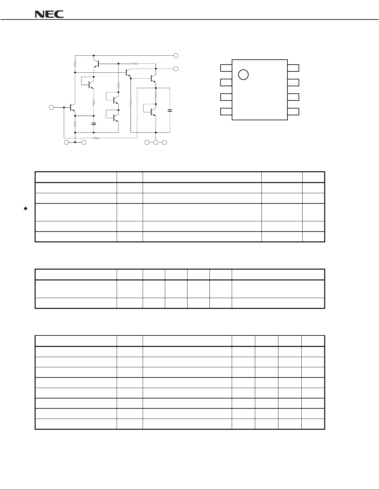
EQUIVALENT CIRCUIT PIN CONNECTIONS
µµµµ
PC1679G
IN 1
67 342
ABSOLUTE MAXIMUM RATINGS
Parameter Symbol Conditions Rating Unit
Supply Voltage V
Input Power P
Power Dissipation P
Operating Ambient Temperature T
Storage Temperature T
8 V
CC
5 OUT
INPUT
1
(Top View)
2GND
3GND
4GND
CC
TA = +25 °C, pin 5, pin 8 6 V
in
TA = +25 °C +10 dBm
D
Mounted on double copper clad 50 × 50 × 1.6 mm
A
epoxy glass PWB (T
A
stg
= +85 °C)
360 mW
45 to +85 °C
−
55 to +150 °C
−
8V
CC
7 GND
6 GND
5 OUTPUT
RECOMMENDED OPERATING RANGE
Parameter Symbol MIN. TYP. MAX. Unit Notice
Supply Voltage V
Operating Ambient Temperature T
ELECTRICAL CHARACTERISTICS (TA = +25 °C, VCC = V
Parameter Symbol Conditions MIN. TYP. MAX. Unit
Circuit Current I
Power Gain G
Noise Figure NF f = 500 MHz
Upper Limit Operating Frequency f
Isolation ISL f = 500 M Hz 29 34
Input Return Loss RL
Output Return Loss RL
Saturated Output Power P
CC
A
CC
P
u
out
O(sat)
4.5 5.0 5.5 V The same voltage should be applied
to pin 5 and 8
45 +25 +85 °C
−
out
= 5.0 V, ZS = ZL = 50
No signal 32 40 49 mA
f = 500 MHz 19.5 21.5 23.5 dB
−
3 dB down below the gain at 0.1 GHz
in
f = 500 MHz 9 12
1.5 1.8
f = 500 MHz 1 3
f = 500 MHz, Pin = +3 dBm +13.5 +15.5
)
ΩΩΩΩ
6.0 8.0 dB
−
−
−
−
−
GHz
dB
dB
dB
dBm
2
Data Sheet P12434EJ4V0DS00
Page 3
µµµµ
PC1679G
TEST CIRCUIT
V
CC
1 800 pF
C
3
L: 20.5 T, 2 mm I.D., 0.25 UEW
L
(about 300 nH)
C
2
50 Ω
OUT
IN
50 Ω
1
C
1 800 pF
8
1
5
1 800 pF
2, 3, 4, 6, 7
INDUCTOR FOR THE OUTPUT PIN
The internal output transistor of this IC consumes 30 mA, to output medium power. To supply current for output
CC
transistor, connect an inductor between the V
pin (pin 8) and output pin (pin 5). Select large value inductance, as
listed above.
The inductor has both DC and AC effects. In terms of DC, the inductor biases the output transistor with minimum
voltage drop to output enable high level. In terms of AC, the inductor make output-port impedance higher to get
enough gain. In this case, large inductance and Q is suitable.
φ
CAPACITORS FOR THE V
Capacitors of 1 800 pF are recommendable as the bypass capacitor for the V
CC
, INPUT AND OUTPUT PINS
CC
pin and the coupling capacitors
for the input and output pins.
The bypass capacitor connected to the VCC pin is used to minimize ground impedance of VCC pin. So, stable bias
can be supplied against VCC fluctuation.
The coupling capacitors, connected to the input and output pins, are used to cut the DC and minimize RF serial
impedance. Their capacitance are therefore selected as lower impedance against a 50 Ω load. The capacitors thus
perform as high pass filters, suppressing low frequencies to DC.
To obtain a flat gain from 100 MHz upwards, 1 800 pF capacitors are used in the test circuit. In the case of under
10 MHz operation, increase the value of coupling capacitor such as 10 000 pF. Because the coupling capacitors are
determined by equation, C = 1/(2 πRfc).
Data Sheet P12434EJ4V0DS00
3
Page 4
TYPICAL CHARACTERISTICS (Unless otherwise specified, TA = +25 °C)
CIRCUIT CURRENT vs. OPERATATING
CIRCUIT CURRENT vs. SUPPLY VOLTAGE
60
No Signal
50
AMBIENT TEMPERATURE
60
No Signal
CC
= 5.0 V
V
50
µµµµ
PC1679G
40
(mA)
CC
30
20
Circuit Current I
10
0
0123456 –60–40–200+20+40+60+80+100
NOISE FIGURE AND INSERTION
POWER GAIN vs. FREQUENCY
25
9
20
8
(dB)
P
15
7
10
6
Noise Figure NF (dB)
5
4
5
Insertion Power Gain G
0
40
(mA)
CC
30
20
Circuit Current I
10
0
Supply Voltage VCC (V) Operating Ambient Temperature T
INSERTION POWER GAIN vs. FREQUENCY
VCC = 5.5 V
G
P
VCC = 5.0 V
VCC = 4.5 V
25
20
(dB)
P
15
VCC = 5.0 V
TA = –45 °C
TA = +25 °C
TA = +85 °C
10
VCC = 5.5 V
5
NF
VCC = 5.0 V
Frequency f (GHz)
VCC = 4.5 V
3.01.00.30.10.030.01
Insertion Power Gain G
0
Frequency f (GHz)
A
(°C)
3.01.00.30.10.030.01
INPUT RETURN LOSS AND OUTPUT
ISOLATION vs. FREQUENCY
0
RETURN LOSS vs. FREQUENCY
+10
VCC = 5.0 VVCC = 5.0 V
–10
–20
–30
(dB)
(dB)
out
in
–10
–20
0
RL
RL
out
in
Isolation ISL (dB)
–40
–50
3.01.00.30.10.030.01
Frequency f (GHz)
4
Data Sheet P12434EJ4V0DS00
–30
Input Return Loss RL
Output Return Loss RL
–40
3.01.00.30.10.030.01
Frequency f (GHz)
Page 5

µµµµ
PC1679G
OUTPUT POWER vs. INPUT POWER
+25
f = 500 MHz
+20
(dBm)
out
+15
VCC = 5.0 V
+10
Output Power P
+5
0
–20 –15 –10 –5 0 +5 +10
VCC = 5.5 V
VCC = 4.5 V
Input Power Pin (dBm)
SATURATED OUTPUT POWER vs. FREQUENCY
+25
Pin = +3 dBm
+20
(dBm)
O(sat)
VCC = 5.5 V
+15
VCC = 5.0 V
+10
VCC = 4.5 V
OUTPUT POWER vs. INPUT POWER
+25
f = 500 MHz
CC
= 5.0 V
V
+20
(dBm)
out
+15
TA = +25 °C
TA = +85 °C
TA = –45 °C
+10
Output Power P
+5
0
–20 –15 –10 –5 0 +5 +10
Input Power Pin (dBm)
THIRD ORDER INTERMODULATION DISTORTION
vs. OUTPUT POWER OF EACH TONE
–60
(dBc)
–50
3
IM
–40
VCC = 5.0 V
f1 = 500 MHz
2
= 502 MHz
f
VCC = 5.5 V
–30
–20
VCC = 4.5 V
+5
Saturated Output Power P
0
Frequency f (GHz)
–10
Third Order Intermodulation Distortion
0
Output Power of Each Tone P
O(each)
+15+10+50–53.01.00.30.10.030.01
(dBm)
Data Sheet P12434EJ4V0DS00
5
Page 6

µµµµ
PC1679G
S-PARAMETER (TA = +25°C, VCC = V
S11-FREQUENCY
out
= 5.0 V)
3.0 G
1.0 G
0.1 G
2.0 G
S22-FREQUENCY
2.0 G
3.0 G
0.1 G
0.5 G
1.0 G
6
Data Sheet P12434EJ4V0DS00
Page 7

TYPICAL S-PARAMETER VALUES
PC1679G
µ
VCC = V
out
= 5.0 V, ICC = 40 mA
µµµµ
PC1679G
FREQUENCY S
MHz MAG. ANG. MAG. ANG. MAG. ANG. MAG. ANG.
100.0000 0.133 177.2 11.167
200.0000 0.154 171.2 11.585
300.0000 0.184 159.6 12.121
400.0000 0.217 147.3 12.690
500.0000 0.247 132.4 13.210
600.0000 0.279 117.7 13.509
700.0000 0.307 102.8 13.902
800.0000 0.333 88.3 13.966
900.0000 0.342 76.4 13.895
1000.0000 0.412 60.4 14.401
1100.0000 0.419 46.1 14.244
1200.0000 0.434 31.7 14.249
1300.0000 0.450 18.1 14.096
1400.0000 0.461 3.2 13.945
1500.0000 0.481
1600.0000 0.486
1700.0000 0.487
1800.0000 0.486
1900.0000 0.479
2000.0000 0.469
2100.0000 0.467
2200.0000 0.454
2300.0000 0.450
2400.0000 0.449
2500.0000 0.443 179.3 7.022 135.4 0.045
2600.0000 0.441 163.8 6.289 130.2 0.037
2700.0000 0.430 149.9 5.800 126.1 0.029
2800.0000 0.426 139.0 5.277 121.8 0.027
2900.0000 0.429 128.2 5.108 116.7 0.027 6.1 0.672 110.0 1.84
3000.0000 0.432 118.6 4.894 114.0 0.025 15.9 0.635 103.2 2.02
3100.0000 0.419 110.7 4.541 107.4 0.028 31.2 0.598 98.0 2.05
11
12.2 13.888
−
27.2 13.645
−
43.7 13.460
−
61.2 13.043
−
78.4 12.509
−
95.6 11.678 179.0 0.057 13.6 0.794
−
113.5 10.720 168.4 0.057 9.9 0.819
−
130.9 9.763 158.2 0.056 3.5 0.840 179.9 0.63
−
148.4 8.754 150.0 0.054
−
165.0 7.849 142.4 0.050
−
21
S
4.7 0.024
−
9.8 0.022
−
16.1 0.018
−
23.9 0.015 4.9 0.669
−
32.2 0.015 20.0 0.681
−
40.9 0.017 35.5 0.680
−
51.0 0.021 42.6 0.674
−
59.8 0.026 44.8 0.659
−
69.5 0.027 42.5 0.628
−
78.5 0.033 52.0 0.646
−
87.9 0.037 46.1 0.636
−
97.3 0.041 42.5 0.635
−
106.9 0.043 41.8 0.640
−
116.9 0.047 35.8 0.655
−
125.9 0.051 34.1 0.664
−
136.5 0.053 30.5 0.691
−
147.3 0.053 27.3 0.707
−
157.9 0.056 21.6 0.742
−
170.0 0.058 17.7 0.771
−
12
S
4.9 0.589
−
10.3 0.620
−
3.0 0.648
−
1.4 0.846 168.7 0.71
−
6.4 0.852 157.1 0.78
−
9.9 0.829 145.9 0.90
−
13.3 0.790 133.6 1.11
−
11.1 0.733 124.7 1.49
−
1.1 0.697 117.2 1.75
−
22
S
3.9 1.40
−
9.7 1.41
−
17.3 1.51
−
25.9 1.63
−
35.1 1.42
−
44.3 1.15
−
53.6 0.88
−
62.0 0.71
−
70.6 0.72
−
75.4 0.48
−
83.6 0.46
−
90.1 0.43
−
97.8 0.41
−
105.0 0.39
−
112.7 0.39
−
120.6 0.39
−
129.2 0.42
−
138.5 0.44
−
147.7 0.48
−
158.3 0.53
−
169.0 0.59
−
K
Data Sheet P12434EJ4V0DS00
7
Page 8

PACKAGE DIMENSIONS
8 PIN PLASTIC SOP (225 mil) (Unit: mm)
85
detail of lead end
P
µµµµ
PC1679G
1
4
A
F
G
S
B
E
D
NOTE
Each lead centerline is located within 0.12 mm of
its true position (T.P.) at maximum material condition.
C
M
M
H
I
L
K
ITEM MILLIMETERS
A
B
C
D 0.42
E
F
G
H
J
K 0.17
L 0.6±0.2
M
N
P3°
I
5.2±0.2
0.85 MAX.
1.27 (T.P.)
+0.08
−0.07
0.1±0.1
1.57±0.2
1.49
6.5±0.3
4.4±0.15
1.1±0.2
+0.08
−0.07
0.12
0.10
+7°
−3°
J
NS
8
Data Sheet P12434EJ4V0DS00
Page 9

µµµµ
PC1679G
NOTE ON CORRECT USE
(1) Observe precautions for handling because of electro-static sensitive devices.
(2) Form a ground pattern as widely as possible to minimize ground impedance (to prevent undesired oscillation).
All the ground pins must be connected together with wide ground pattern to decrease impedance difference.
(3) The bypass capacitor should be attached to VCC line.
(4) The inductor must be attached between VCC and output pins. The inductance value should be determined in
accordance with desired frequency.
(5) The DC cut capacitor must be attached to input pin.
RECOMMENDED SOLDERING CONDITIONS
This product should be soldered under the following recommended conditions. For soldering methods and
conditions other than those recommended below, contact your NEC sales representative.
Soldering Method Soldering Conditions Recommended Condition Symbol
Infrared Reflow Package peak temperature: 235 °C or below
Time: 30 seconds or less (at 210 °C)
Count: 3, Exposure limi t: None
VPS Package peak temperature: 215 °C or below
Time: 40 seconds or less (at 200 °C)
Count: 3, Exposure limi t: None
Wave Soldering Soldering bath temperature: 260 °C or below
Time: 10 seconds or less
Count: 1, Exposure limi t: None
Partial Heating Pin temperature: 300 °C
Time: 3 seconds or less (per side of device)
Exposure limit: None
After opening the dry pack, keep it in a place below 25 °C and 65 % RH for the allowable storage period.
Note
Note
Note
Note
Note
IR35-00-3
VP15-00-3
WS60-00-1
–
Caution Do not use different soldering methods together (except for partial heating).
For details of recommended soldering conditions for surface mounting, refer to information document
SEMICONDUCTOR DEVICE MOUNTING TECHNOLOGY MANUAL (C10535E).
Data Sheet P12434EJ4V0DS00
9
Page 10

[MEMO]
µµµµ
PC1679G
10
Data Sheet P12434EJ4V0DS00
Page 11

[MEMO]
µµµµ
PC1679G
Data Sheet P12434EJ4V0DS00
11
Page 12

µµµµ
PC1679G
NESAT (NEC Silicon Advanced Technology) is a trademark of NEC Corporation.
• The information in this document is subject to change without notice. Before using this document, please
confirm that this is the latest version.
• No part of this document may be copied or reproduced in any form or by any means without the prior written
consent of NEC Corporation. NEC Corporation assumes no responsibility for any errors which may appear in
this document.
• NEC Corporation does not assume any liability for infringement of patents, copyrights or other intellectual property
rights of third parties by or arising from use of a device described herein or any other liability arising from use
of such device. No license, either express, implied or otherwise, is granted under any patents, copyrights or other
intellectual property rights of NEC Corporation or others.
• Descriptions of circuits, software, and other related information in this document are provided for illustrative
purposes in semiconductor product operation and application examples. The incorporation of these circuits,
software, and information in the design of the customer's equipment shall be done under the full responsibility
of the customer. NEC Corporation assumes no responsibility for any losses incurred by the customer or third
parties arising from the use of these circuits, software, and information.
• While NEC Corporation has been making continuous effort to enhance the reliability of its semiconductor devices,
the possibility of defects cannot be eliminated entirely. To minimize risks of damage or injury to persons or
property arising from a defect in an NEC semiconductor device, customers must incorporate sufficient safety
measures in its design, such as redundancy, fire-containment, and anti-failure features.
• NEC devices are classified into the following three quality grades:
"Standard", "Special", and "Specific". The Specific quality grade applies only to devices developed based on a
customer designated "quality assurance program" for a specific application. The recommended applications of
a device depend on its quality grade, as indicated below. Customers must check the quality grade of each device
before using it in a particular application.
Standard: Computers, office equipment, communications equipment, test and measurement equipment,
audio and visual equipment, home electronic appliances, machine tools, personal electronic
equipment and industrial robots
Special: Transportation equipment (automobiles, trains, ships, etc.), traffic control systems, anti-disaster
systems, anti-crime systems, safety equipment and medical equipment (not specifically designed
for life support)
Specific: Aircraft, aerospace equipment, submersible repeaters, nuclear reactor control systems, life
support systems or medical equipment for life support, etc.
The quality grade of NEC devices is "Standard" unless otherwise specified in NEC's Data Sheets or Data Books.
If customers intend to use NEC devices for applications other than those specified for Standard quality grade,
they should contact an NEC sales representative in advance.
M7 98. 8
 Loading...