

Page 1

INTEGRATED CIRCUITS
DATA SH EET
TEA6821T
ICE car radio
Preliminary specification
File under Integrated Circuits, IC01
September 1993
Page 2

Philips Semiconductors Preliminary specification
ICE car radio TEA6821T
FEATURES
General
• FM mixer for conversion from FM IF
= 72.2 MHz to FM
1
IF2 = 10.7 MHz
• AM mixer for conversion from AM IF1 = 10.7 MHz to AM
IF2 = 450 kHz
• FM IF gain stage
• Crystal oscillator providing mixer frequencies and
references for IF count and stereo decoder
• FM quadrature demodulator with automatic centre
frequency adjust and THD compensation
• Level and multipath and noise detectors
• Soft mute
• Stereo noise cancelling and variable de-emphasis
• PLL stereo decoder
• Noise blanker
• AM IF amplifier and demodulator
• I2C-bus transceiver
• IF count for AM and FM
• Reference frequency generation for PLL synthesizer
• Reduced external components
• SW applicable.
Stereo decoder
• Adjustment-free PLL-VCO
• Pilot depending mono/stereo switching
• Analog control of mono/stereo blend
• Adjacent channel noise suppression (114 kHz)
• Pilot canceller
• Analog control of de-emphasis
• Integrated low-pass filters for 190 kHz adjacent channel
interferences and signal delay for interference
absorption circuit.
GENERAL DESCRIPTION
The TEA6821T together with the TEA6810T / TEA6811T
forms an AM/FM electronic tuned car radio in a double
conversion receiver concept for European, American and
Japanese frequency range.
QUICK REFERENCE DATA
SYMBOL PARAMETER CONDITIONS MIN. TYP. MAX. UNIT
V
s1
V
s1
I
s1
I
s1
V
s2
V
s2
I
s2
I
s2
supply voltage 1 (pins 56 and 28) note 1 7 8.5 10 V
operating range 8.1 8.5 8.9 V
supply current 1 FM − 28 − mA
supply current 1 AM − 24 − mA
supply voltage 2 (pin 5) note 1 4.5 5.0 5.5 V
operating range 4.75 5.0 5.25 V
supply current 2 FM − 31 − mA
supply current 2 AM − 28 − mA
S+N/N signal-to-noise AM m = 0.3 − 57 − dB
THD distortion AM − 12%
S+N/N signal-to-noise FM ∆f = 22.5 kHz at pins 43 and 47 66 72 − dB
THD distortion FM ∆f = 75 kHz − 0.1 0.35 %
α channel separation (adjusted) 40 −−dB
T
amb
operating ambient temperature −40 − +85 °C
Note to the quick reference data
1. IC is functional, specified parameters may deviate from limits which are valid for operating range.
September 1993 2
Page 3

Philips Semiconductors Preliminary specification
ICE car radio TEA6821T
ORDERING INFORMATION
TYPE
NUMBER
TEA6821T VSO56
NAME DESCRIPTION VERSION
PACKAGE
plastic very small outline package; 56 leads
SOT190-1
September 1993 3
Page 4
Philips Semiconductors Preliminary specification
ICE car radio TEA6821T
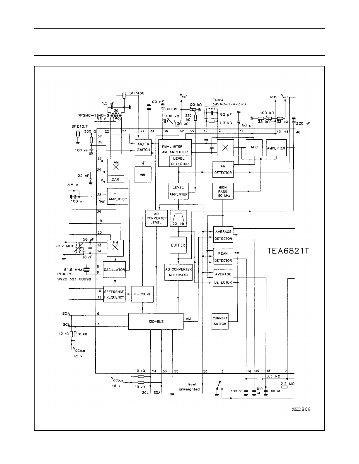
Fig.1 Block diagram (continued in Fig.2).
September 1993 4
Page 5
Philips Semiconductors Preliminary specification
ICE car radio TEA6821T
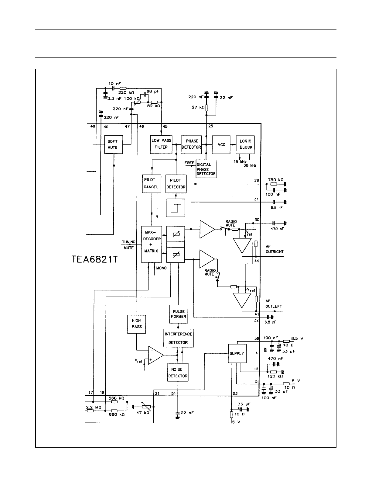
Fig.2 Block diagram (continued from Fig.1).
September 1993 5
Page 6
Philips Semiconductors Preliminary specification
ICE car radio TEA6821T
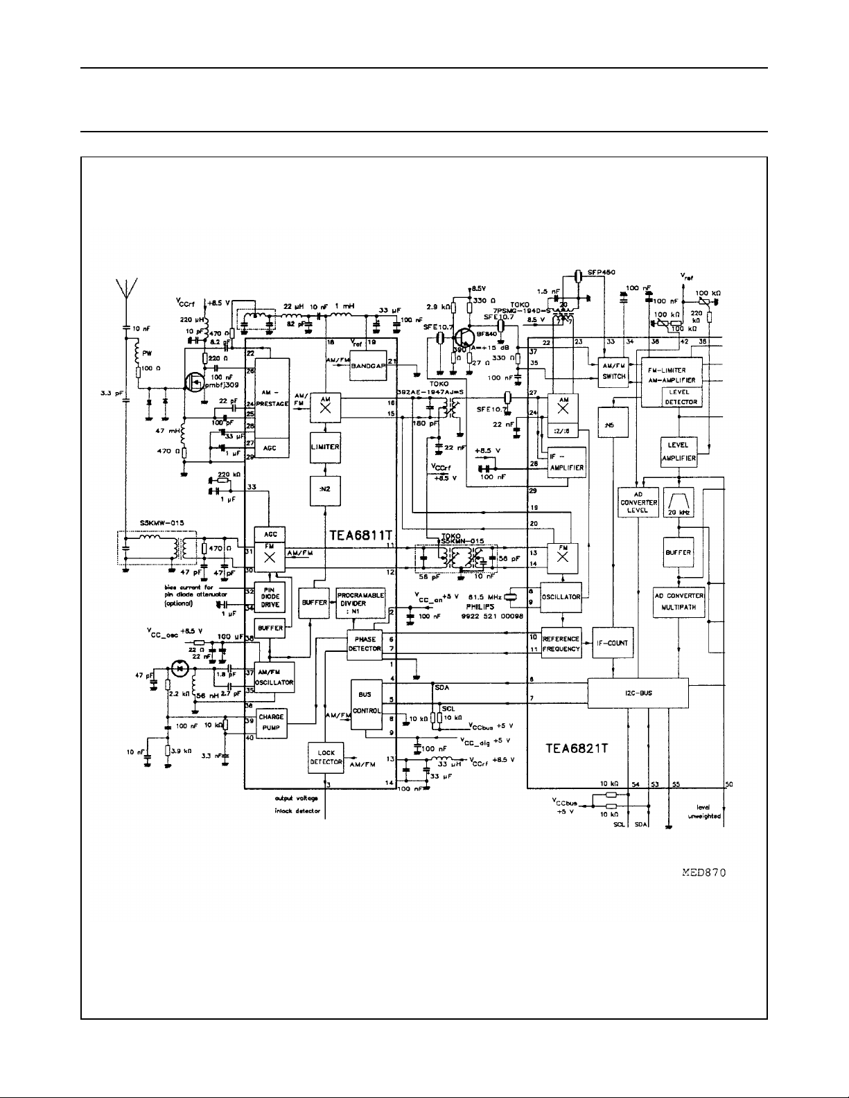
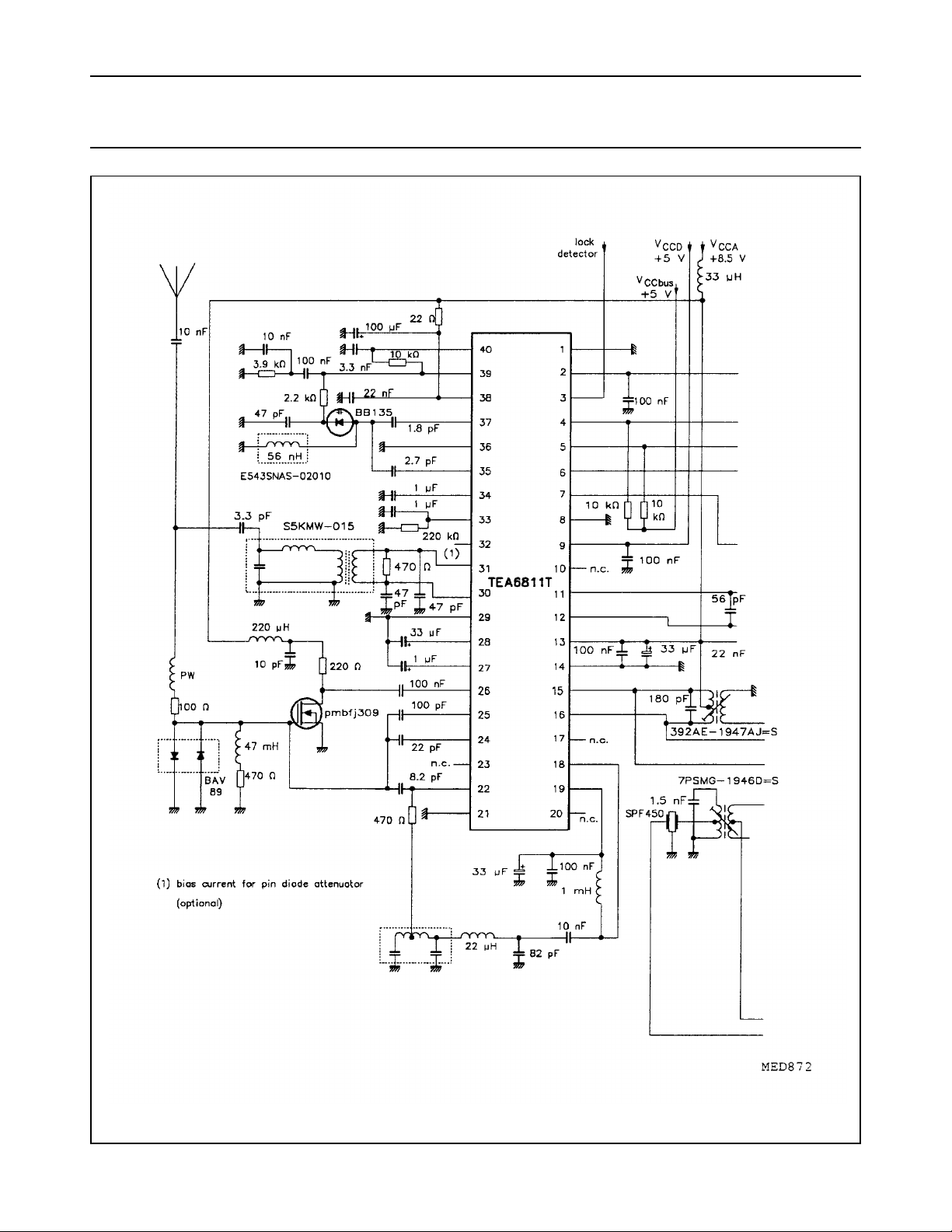
Fig.3 ICE91 application diagram (continued in Fig.4).
September 1993 6
Page 7
Philips Semiconductors Preliminary specification
ICE car radio TEA6821T
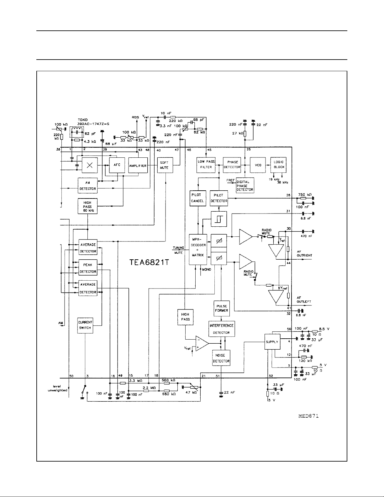
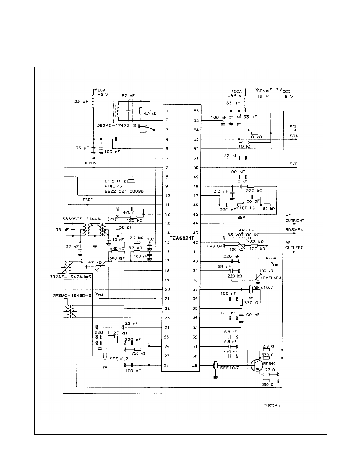
Fig.4 ICE91 application diagram (continued from Fig.3).
September 1993 7
Page 8
Philips Semiconductors Preliminary specification
ICE car radio TEA6821T
Fig.5 AM/FM car radio receiver with TEA6811T and TEA6821T (continued in Fig.6).
September 1993 8
Page 9
Philips Semiconductors Preliminary specification
ICE car radio TEA6821T
Fig.6 AM/FM car radio receiver with TEA6811T and TEA6821T (continued from Fig.5).
September 1993 9
Page 10

Philips Semiconductors Preliminary specification
ICE car radio TEA6821T
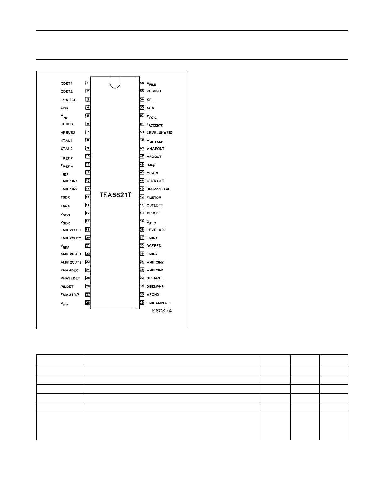
PINNING
SYMBOL PIN DESCRIPTION
QDET1 1 demodulator tank
QDET2 2 demodulator tank
TSWITCH 3 time switch
GND 4 analog ground
V
P5
5 5 V supply voltage
HFBUS1 6 HF bus, pull-up to 5 V
HFBUS2 7 HF bus, pull-up to 5 V
XTAL1 8 crystal oscillator
XTAL2 9 crystal oscillator
F
F
I
REF
REFP
REFN
10 PLL reference frequency
11 PLL reference frequency
12 reference current
FMIF1IN1 13 70 MHz FM-IF input
FMIF1IN2 14 70 MHz FM-IF input
TSDR 15 time constant for SDR
TSDS 16 time constant for SDS
V
V
SDS
SDR
17 SDS control voltage
18 SDR control voltage
FMIF2OUT1 19 FM mixer output
FMIF2OUT2 20 FM mixer output
V
REF
21 reference voltage
AMIF2OUT1 22 AM mixer output
AMIF2OUT2 23 AM mixer output
FMAMDEC 24 FM/AM 10.7 MHz decoupling
PHASEDET 25 phase detector
PILDET 26 pilot detector
FMAM10.7 27 FM/AM 10.7 MHz input
V
PIF
28 VP IF amplifier
SYMBOL PIN DESCRIPTION
FMIFAMPOUT 29 FM-IF amplifier output
AFGND 30 AF ground
DEEMPHR 31 de-emphasis capacitor right
DEEMPHL 32 de-emphasis capacitor left
AMIF2IN1 33 AM IF2 input 1
AMIF2IN2 34 AM IF2 input 2
FMIN2 35 FM limiter input
DCFEED 36 DC feed FM limiter
FMIN1 37 FM limiter input
LEVELADJ 38 level adjust
C
AFC
39 AFC capacitor
MPBUF 40 multipath buffer time constant
OUTLEFT 41 AF output left
FMSTOP 42 FMSTOP adjust
RDS/AMSTOP 43 MPX for RDS/AMSTOP adjust
OUTRIGHT 44 AF output right
MPXIN 45 stereo decoder MPX input
IAC
IN
46 IAC input
MPXOUT 47 FM demodulator MPX output
AMAFOUT 48 AM demodulator AF output
V
MUTAML
49 mute voltage / AM level
LEVELUNWEIG 50 level unweighted
I
ACCONTR
V
PDIG
51 IAC control voltage
52 VP digital
SDA 53 SDA, pull-up to 5 V
SCL 54 SCL, pull-up to 5 V
BUSGND 55 bus ground
V
P8.5
56 VP 8.5 V
September 1993 10
Page 11
Philips Semiconductors Preliminary specification
ICE car radio TEA6821T
Fig.7 Pin configuration.
LIMITING VALUES
In accordance with the Absolute Maximum Rating System (IEC 134).
SYMBOL PARAMETER MIN. MAX. UNIT
V
V
V
T
T
V
s1
s2
s3
stg
amb
ESD
supply voltage 1 (pins 56 and 28) −0.3 +12 V
supply voltage 2 (pin 5) −0.3 +6.5 V
supply voltage 3 (pin 52) −0.3 +6.5 V
storage temperature −55 +150 °C
operating ambient temperature −40 +85 °C
electrostatic handling (note 1)
for pins 8 and 9 −±100 V
for other pins −±300 V
Note to the limiting values
1. Charge device model class B: discharging a 200 pF capacitor through a 0 Ω series resistor.
September 1993 11
Page 12

Philips Semiconductors Preliminary specification
ICE car radio TEA6821T
CHARACTERISTICS
V
56-4=V28-4
= 8.5 V, V
SYMBOL PARAMETER CONDITIONS MIN. TYP. MAX. UNIT
Current consumption
I
s1
I
56
I
28
I
+ I
19
20
I
s1
I
56
I
+ I
22
23
I
s2
I
s3
supply current 1 FM 24 30 36 mA
supply current 1at pin 56 16 20 24 mA
supply current 1 at pin 28 2.4 3.0 3.6 mA
supply current 1 at pins 19 and 20 4.8 6.0 7.2 mA
supply current 1 AM 18 24 30 mA
supply current 1at pin 56 9.5 12 15 mA
supply current 1 at pins 22 and 23 8 10 12.5 mA
supply current 2 at pin 5 FM 18 21 25 mA
supply current 3 at pin 52 8 10 12 mA
FM IF path
5-4
= V
52-55
= 5 V, T
= +25 °C unless otherwise specified.
amb
AM 14 17 21 mA
FM mixer
R
13-14
C
13-4,C14-4
R
opt
R
19-20
, C
C
19-4
20-4
I
19IF2/V13-14IF1
I
, I
19
20
input resistance 5 7 − kΩ
input capacitance − 3 4.5 pF
optimum generator resistance − 1.2 − kΩ
output resistance 15 20 − kΩ
output capacitance − 57pF
conversion gain 1.65 1.9 2.2 mS
mixer bias current 2.4 3.0 3.6 mA
mixer leakage current in AM position −−2µA
V
19-20
maximum output voltage
12.0 14.0 − V
(peak-to-peak value)
IP3 third order intermodulation 114 124 − dBµV
Oscillator
f
osc
oscillator frequency − 61.5 − MHz
oscillator spread −−250 Hz
∆f
/∆T temperature dependence of
osc
oscillator frequency
R
1
C
0
crystal motional resistance −−70 Ω
crystal shunt capacitance −−5pF
crystal type PHILIPS
9922 521 00098
− 30 − ppm/K
FM IF2 amplifier
V
29-4/V27-24
amplifier gain loaded with 330 Ω;
8 1012dB
see Fig.9
V
27-24
maximum input voltage for 1 dB
80 110 − mV
compression point (RMS value)
September 1993 12
Page 13

Philips Semiconductors Preliminary specification
ICE car radio TEA6821T
SYMBOL PARAMETER CONDITIONS MIN. TYP. MAX. UNIT
V
29-4
R
27-24
C
, C
27-4
24-4
R
29-4
C
29-4
FM IF2 limiter
V
1-2/V37-35
C
37-4
R
1-2
C
1-2
V
1-2
maximum output voltage
220 270 − mV
(RMS value)
input resistance 300 330 360 Ω
input capacitance −−5pF
output resistance 300 330 360 Ω
output capacitance −−5pF
limiter gain see Fig.10 − 74 − dB
input capacitance −−5pF
output resistance −−1.0 kΩ
output capacitance 10 15 20 pF
limiter output voltage
500 700 − mV
(peak-to-peak value)
FM demodulator
f
= 1kHz; deviation = 22.5 kHz; Rg= 50 Ω; V
mod
= 10 mV; with de-emphasis = 50 µS; coil quality = 15 unless
37-35
otherwise specified.
V
R
47-4
47out
MPX output (RMS value) 160 200 240 mV
output resistance −−500 Ω
B AF bandwidth 200 −−kHz
V
R
43-4
43out
MPX output for RDS (RMS value) 160 200 240 mV
output resistance −−500 Ω
B AF bandwidth 200 −−kHz
V
V
37-35
37-35
start of limiting (RMS value) αAF = −3 dB − 40 60 µV
input voltage for
signal-plus-noise-to-noise ratio
(RMS value)
see Fig.11 for pin 47
(MPXOUT) and Fig.12 for
pin 43 (RDS/AMSTOP)
S+N/N = 26 dB − 40 55 µV
S+N/N = 46 dB − 100 140 µV
S + N/N signal-plus-noise-to-noise ratio 66 72 − dB
V
43FM/V43AM
suppression ∆f = 22.5 kHz; 55 60 − dB
f
= 1 kHz;
modAM
mAM= 30%;
= 3 mV to 300 mV
V
37-35
V
47FM/V47AM
suppression V
= 1 mV to 300 mV 55 60 − dB
37-35
September 1993 13
Page 14

Philips Semiconductors Preliminary specification
ICE car radio TEA6821T
SYMBOL PARAMETER CONDITIONS MIN. TYP. MAX. UNIT
THD total harmonic distortion detuning ≤ 50 kHz;
∆f = 75 kHz; f
without de-emphasis
L
= typical value
demod
pin 43 − 0.1 0.35 %
V
= 300 µV to 800 mV
37-35
pin 47 − 0.1 0.35 %
V
= 1 mV to 800 mV
37-35
∆V
43AFCdisabled
/∆V
43AFCactive
demodulator frequency control
(AFC) efficiency at 100 kHz detune
from exact tuning
∆V
43
residual DC-offset ∆L
= typical value;
demod
10 µV<V
80 µV<V
Unweighted level voltage
BW
50
R
out50
V
50-4
V/20 dB slope of level unweighted voltage
/VK temperature dependence V
∆V
50-4
Adjust of level unweighted voltage and V
∆V
50
∆V
/∆V
50-4
R
38
V
38-4
bandwidth 500 −−kHz
output resistance −−100 Ω
level unweighted voltage see Fig.13; V38 = 2.52 V;
V
≤ 2.5 µV 1.8 2.4 3.2 V
37-35
V
= 1.0 mV 2.7 3.4 4.7 V
37-35
V
≤ 100 µV
37-35
∆V
/∆V
50-4
37-35
; typical adjusting range see Figs 14 and 17.
mutaml
adjusting range V
adjusting gain −−0.9 −−
38-4
(RMS) < 300 mV
= 1 mV − 4.0 − mV/VK
37-35
= 1 mV (RMS) −±2−V
37-35
input resistance − 80 − kΩ
internal bias voltage − 2.6 − V
Muting dependence on adjust of level unweighted voltage; typical curve see Fig.15.
α = V
∆α /∆V
43/V47
49
start of mute V49/V21 = 0.6 − 3 −−
mute slope α= −6 dB − 25 − dB/V
Soft mute, time constant control, mono/stereo blend and high-cut control
Time constant control (see application diagram Fig.3): Slow or fast attack and decay time constants for soft mute,
mono/stereo and high-cut control can be chosen connecting pin 3 to GND or pin 21.
Mute voltage: The static mute voltage follows the level unweighted voltage as function of FM IF
adjust voltage V
of Tswitch. Typical curve for mute voltage dependence on V
V
49-4
. It additionally depends on multipath level, noise (adjacent channel interferences) and the position
38-4
see Fig.16.
37-35
mute voltage V38 = 2.52 V;
V
≤ 2.5 µV 1.8 2.2 3.2 V
37-35
= 1.0 mV 2.7 3.3 4.7 V
V
37-35
= 1 kHz
mod
30 34 − dB
<80µV − 100 1000 mV
37-35
< 800 mV − 10 30 mV
37-35
0.75 0.845 0.95 V
voltage and level
2
September 1993 14
Page 15

Philips Semiconductors Preliminary specification
ICE car radio TEA6821T
SYMBOL PARAMETER CONDITIONS MIN. TYP. MAX. UNIT
V/20 dB slope of mute voltage ∆V
∆V
/VK temperature dependence V
49-4
Attack and decay time for mute voltage.
I
49
charge current pin 3 connected to GND − 3.0 −µA
discharge current −−3.6 −µA
charge current pin 3 connected to pin 21 − 130 −µA
discharge current −−160 −µA
∆f muting activated by 60 kHz
FM interference
Time constant for mono/stereo blend voltage. The mono/stereo blend voltage is generated as a function of FM IF
voltage, multipath level, noise and position of Tswitch.
I
16
charge current V
discharge current pin 3 connected to GND −−18 −µA
charge current V
discharge current pin 3 connected to pin 21 −−800 −µA
m mono/stereo blend activated by
20 kHz AM interference
∆f mono/stereo blend activated by
60 kHz FM interference
Time constant for high-cut control voltage (SDR). The high-cut control voltage is generated as a function of FM IF
voltage, multipath level, noise and position of Tswitch.
I
15
charge current V
discharge current pin 3 connected to GND −−0.44 −µA
charge current V
discharge current pin 3 connected to pin 21 −−44 −µA
m high-cut control activated by 20 kHz
AM interference
∆f high-cut control activated by 60 kHz
FM interference
49-4
/∆V
37-35V37-35
≤ 100 µV
0.75 0.845 0.95 V
(RMS) < 300 mV
= 1 mV − 4.0 − mV/VK
37-35
pin 3 connected to GND;
V
= 3 mV;
37-35
V49 < 2 V; f
= 3 mV; − 0.5 −µA
37-35
= 3 mV; − 26 −µA
37-35
V
< 2 V; V
16
R
> 50 MΩ;
L16
= 20 kHz; pin 3
f
mod
= 60 kHz
mod
37-35
= 3 mV;
− 30 − kHz
− 45 − %
connected to GND
pin 3 connected to pin 21 − 40 − %
V
< 3 V; V
16
R
> 50 MΩ;
L16
f
= 60 kHz; pin 3
mod
37-35
= 3 mV;
− 30 − kHz
connected to GND
pin 3 connected to pin 21 − 22 − kHz
= 3 mV; − 0.4 −µA
37-35
= 3 mV; − 41 −µA
37-35
V
R
f
mod
15
L15
< 2 V; V
> 50 MΩ;
= 20 kHz;
37-35
= 3 mV;
pin 3 connected to GND − 40 − %
pin 3 connected to pin 21 − 35 − %
V
R
f
mod
15
L15
< 2 V; V
> 50 MΩ;
= 60 kHz;
37-35
= 3 mV;
pin 3 connected to GND − 25 − kHz
pin 3 connected to pin 21 − 20 − kHz
2
2
September 1993 15
Page 16

Philips Semiconductors Preliminary specification
ICE car radio TEA6821T
SYMBOL PARAMETER CONDITIONS MIN. TYP. MAX. UNIT
Multipath detector
f
MP
B
MP
Reference voltage
V
21-4
∆V
21-4
I
21
AM IF path
AM mixer; f
R
27-24
C
27-24
R
22-23
C
22-23
I
22IF2/V27-24IF1
I
, I
22
23
V
22-23
IP3 third order intermodulation − 137 − dBµV
multipath detector band-pass centre
− 20 − kHz
frequency
band-pass bandwidth 7.0 −−kHz
output voltage I21 = −1 mA 4.5 5.1 5.7 V
temperature dependence − 3.3 − mV/VK
output current −−1mA
= 10.7 MHz; f
IF1
= 450 kHz; (see Fig.18)
IF2
input resistance 300 330 360 Ω
input capacitance − 58pF
output resistance 10.0 20.0 − kΩ
output capacitance − 510pF
conversion gain 2.2 2.7 3.4 mS
mixer bias current 4.0 5.0 6.0 mA
mixer leakage current in FM position −−2µA
maximum output voltage
12 15 − V
(peak-to-peak value)
AM oscillator
The AM oscillator signal is generated by division of the 61.5 MHz crystal oscillator.
Two divider ratios programmable via I
AM detector f
V
48-4
V
33-34
= 450 kHz; f
AMIF2
AF output level (RMS value) R
sensitivity (RMS value) S+N/N = 26 dB − 150 250 µV
2
C-bus: division by 6 (AM IF1 = 10.7 MHz), division by 2 (AM IF1 = 30 MHz)
= 400 Hz; m = 30%
mod
> 500 kΩ; 190 240 290 mV
L48
300 µV ≤ V
33-34
≤ 300 mV
S+N/N = 46 dB − 500 700 µV
S+N/N signal-plus-noise-to-noise ratio 54 57 − dB
THD total harmonic distortion m = 0.8;
1 mV ≤ V
V
R
C
R
C
33-34
33-34
24-23
48out
48out
AM IF2 minimum input (RMS value) THD ≤ 5%; m = 0.8 −−500 µV
maximum input (RMS value) 800 −−mV
AM IF
2
IF2 input resistance 1.8 2.0 2.2 kΩ
IF2 input capacitance − 10 15 pF
output resistance 27 33 39 kΩ
output capacitance −−10 pF
24-23
≤ 300 mV
− 1.0 3.0 %
typical AM level curve see Fig.19
Stereo decoder; note 1
Input signal (∆f = 75 kHz) V
(p-p) = 1.7 V; modulation frequency f
MPX
= 1 kHz; de-emphasis time constant
mod
τ =50µs; nominal input resistor (pin 45) Ri = 168 kΩ.
September 1993 16
Page 17

Philips Semiconductors Preliminary specification
ICE car radio TEA6821T
SYMBOL PARAMETER CONDITIONS MIN. TYP. MAX. UNIT
MPX input overdrive margin THD = 1% 4 −−dB
V
, V
44-4
41-4
V
44-4/V41-4
R
, R
o44
o41
R
Imin
I
, I
44
41
V
, V
44-4
41-4
α channel separation (adjusted;
THD total harmonic distortion − 0.1 0.3 %
S+N/N signal-plus-noise-to-noise ratio f = 20 Hz to 20 kHz 74 80 − dB
Carrier and harmonic suppression at the output (note to the stereo decoder).
α
19
α
38
(4)
α
57
α
76
(2)
α
2
(3)
α
3
(4)
α
57
(5)
α
67
(6)
α
114
(7)
α
190
α
rr
Mono/stereo control
V
ipil
∆V
ipil
The stereo decoder can be set to mono via the I
Pilot presence indication via I
External Mono/stereo control
V
− 0.75V21control voltage channel separation see Fig.21
17
Muting functions (mute via I
α
mute
, ∆V
∆V
44
41
α
mute
∆V
, ∆V
44
41
AF output voltage (RMS value) 800 900 1000 mV
difference of output voltage −−±1dB
output resistor −−130 Ω
minimum load resistor 12 −−kΩ
maximum output current 150 −−µA
DC output voltage 3.3 3.8 4.3 V
40 −−dB
a typical roll-off at f
= 38 kHz of
MPX
1 dB is internally compensated)
pilot signal f = 19 kHz − 50 − dB
subcarrier f = 38 kHz − 50 − dB
f = 57 kHz − 46 − dB
f = 76 kHz − 60 − dB
intermodulation f
= 10 kHz; f
mod
f
= 13 kHz; f
mod
= 1 kHz − 60 − dB
spur
= 1 kHz − 58 − dB
spur
traffic radio (ARI) f = 57 kHz − 70 − dB
subsidiary communications
f = 67 kHz 70 −−dB
authorization
adjacent channel frequency f = 114 kHz − 80 − dB
f = 190 kHz − 70 − dB
ripple rejection at output fr = 100 Hz; Vr = 100 mV
− 30 − dB
eff
pilot threshold voltage stereo on − 24 30 mV
mono on 8 20 − mV
switch hysteresis V
2
C-bus
ion/Vioff
2
C-bus
− 2 − dB
α = 6 dB −−80 − mV
α = 16 dB −−40 − mV
2
C-bus)
tuned mute 60 −−dB
DC offset voltage −50 − +50 mV
radio mute (in combination with
80 −−dB
tuned mute)
DC offset voltage −300 − +300 mV
September 1993 17
Page 18

Philips Semiconductors Preliminary specification
ICE car radio TEA6821T
SYMBOL PARAMETER CONDITIONS MIN. TYP. MAX. UNIT
High-cut control (see Fig.22)
τ
deemph
V
− 0.75V21control voltage τ
18
The nominal de-emphasis value can be changed to 75 µs with C
Voltage controlled oscillator
The VCO is adjusted by means of a digital auxiliary PLL.
f
osc
Noise blanker
Interference detection at pin 50 level unweighted or MPXOUT (pin 47)
T
sup
f
c
IAC control
I
51
V
pulse
(pin 51) trigger threshold measured with
∆V
DC
V
(pin 46) VDC(pin 51) = 7.7 V − 10 − mV
tr
∆V
(pin 51) V
DC
(pin 46) VDC(pin 51) = 6.7 V − 100 − V
V
tr
I
os
control range of de-emphasis 50 − 80 µs
= 50 µs0−−mV
deemph
τ
= 80 µs −−300 − mV
deemph
, C32 = 10 nF.
31
oscillator frequency range 450 456 462 kHz
interference suppression time − 40 50 µs
high-pass input filter for interference
3 dB frequency 150 200 250 kHz
pulse, 2nd order
charge current (into 4 V) 5.0 10 18 µA
discharge current (from 8.5 V) −0.5 −1.0 −1.8 mA
trigger sensitivity τ
f
= 250 kHz
int
gate input offset current at pins 31
= 10 µs −−20 mV
pulse
V
(pin 46) = 10 mV − 200 − mV
noise
(pin 46) = 100 mV − 2.3 − V
noise
− 20 50 nA
and 32 during suppression pulse
duration
September 1993 18
Page 19

Philips Semiconductors Preliminary specification
ICE car radio TEA6821T
Notes to the characteristics
1. By changing the value of the input resistor at pin 12 the MPX input can be adapted to the level of the FM demodulator
output (see Fig.20). A 3rd order low-pass filter fg = 90 kHz at the MPX input provides extra 190 kHz ACI suppression.
For AM the VCO is switched off. Interference gate at MPX demodulator outputs.
2.
α
2
α
3.
3
α
4.
57
5.
α
67
α
6.
114
α
7.
190
V0signal()at 1 kHz()
----------------------------------------------------------------------spurious()at 1 kHz()
V
0
f
s
V0signal()at 1 kHz()
----------------------------------------------------------------------spurious()at 1 kHz()
V
0
signal()at 1 kHz()
V
ARI()
=
--------------------------------------------------------------------------------------------------V
0
spurious()at 1 kHz 23 Hz±()
0
f
s
V0signal()at 1 kHz()
-----------------------------------------------------------------------V
spurious()at 9 kHz()
0
V0signal()at 1 kHz()
-----------------------------------------------------------------------spurious()at 4 kHz()
V
0
V0signal()at 1 kHz()
-----------------------------------------------------------------------spurious()at 4 kHz()
V
0
2 x10 kHz()19 kHz–=;=
313kHz×()38 kHz–=;=
238kHz×()67 kHz–=;=
f
s
110 kHz 3 38kHz×()–=;=
f
s
186 kHz 5 38 kHz×()–=;=
f
s
September 1993 19
Page 20

Philips Semiconductors Preliminary specification
ICE car radio TEA6821T
Fig.8 Test circuit FM mixer.
Fig.9 Test circuit IF amplifier.
Fig.10 Test circuit limiter gain.
September 1993 20
Page 21

Philips Semiconductors Preliminary specification
ICE car radio TEA6821T
Fig.11 Signal and noise of muted MPX voltage.
Fig.12 Signal and noise of unmuted MPX voltage.
September 1993 21
Page 22

Philips Semiconductors Preliminary specification
ICE car radio TEA6821T
Fig.13 Level unweighted voltage (typical curve).
Fig.14 Adjustment range level unweighted voltage.
September 1993 22
Page 23

Philips Semiconductors Preliminary specification
ICE car radio TEA6821T
Fig.15 Muting dependence on adjust of level unweighted voltage (typical curve).
Fig.16 Typical mute voltage as function of FM IF2voltage.
September 1993 23
Page 24

Philips Semiconductors Preliminary specification
ICE car radio TEA6821T
Fig.17 Adjustment range mute voltage.
Fig.18 Test circuit AM mixer.
September 1993 24
Page 25

Philips Semiconductors Preliminary specification
ICE car radio TEA6821T
Fig.19 Signal, noise and distortion of AM AF output voltage and AM level voltage (typical curve).
September 1993 25
Page 26

Philips Semiconductors Preliminary specification
ICE car radio TEA6821T
Fig.20 Adaption of MPX input to FM-demodulator output level by variation of the input resistor.
Fig.21 Channel separation as function of control voltage.
September 1993 26
Page 27

Philips Semiconductors Preliminary specification
ICE car radio TEA6821T
Fig.22 High-cut as function of control voltage.
I2C-BUS SPECIFICA TION AND I2C-BUS CONTROLLED FUNCTIONS
2
I
C-bus specification
The standard I2C-bus specification is expanded by the
following definitions. Structure of the I2C-bus logic: slave
transceiver with auto increment and expansion to switch a
direct transfer of all transmissions to an output for the radio
front end IC (TEA6810T respectively TEA6811T).
Subaddresses are not used. Data transfer to the
TEA6821T Data sequence: address byte 1 byte 2
The data transfer has to be only in this order. The transfer
direction of the data bytes is defined by the LSB of the
address. The data becomes valid at the output of the
internal latches with the acknowledge of each byte. A stop
condition after any byte can shorten transmission times.
When writing to the transceiver by using the stop condition
before completion of the whole transfer:
• The remaining bytes will contain the old information
• If the transfer of a byte was not completed, this byte is
lost and the previous information is available.
Data transfer to an output of the front end IC.
A data bit in the transceiver of the TEA6821T enables or
disables a direct transfer of all transmissions to an
interface stage for the front end IC.
For a transmission to the front end IC the address and the
data format of the front end IC has to be used.
Hint: The pull-up resistors for the front end interface (pins
6 and 7) should not be connected to the 5 V supply voltage
of the front end IC, otherwise a bus pull-down (pin 53) can
occur during switching off the front end supply when the
interface stage is enabled.
Data transfer to the IF IC (TEA6821T) is independent of
the state of interface stage for the front end IC.
September 1993 27
Page 28

Philips Semiconductors Preliminary specification
ICE car radio TEA6821T
General specification
bus address of the TEA6821T 1100 001X
subaddress not used
hardware (pin) programmable address bits not available
default settings by power-on reset radio mute and 40 ms IF count time is enabled,
all other bits are random
2
C-bus data
I
Data to be received by the IC
data byte 1 bit 0 switch for mono: bit 0 = 1; stereo: bit 0 = 0
bit 1 LSB reference frequency for synthesizer; see Table 1
bit 2 reference frequency for synthesizer; see Table 1
bit 3 MSB reference frequency for synthesizer; see Table 1
bit 4 tuning mute, bit 4 = 1: off; bit 4 = 0: on
bit 5 SDS/SDR hold, bit 5 = 1: off; bit 5 = 0: on
bit 6 radio mute, bit 6 = 1: off; bit 6 = 0: on
2
bit 7 I
data byte 2 bit 0 AM/FM, bit 0 = 0: AM; bit 0 = 1: FM
bit 1 divider for AM mixer, bit 1 = 0: division by 2; bit 1 = 1: division by 6
bit 2 measure time IF count, bit 2 = 0: 40 ms; bit 2 = 1: 4 ms
bit 3 SDR off, bit 3 = 0: SDR off; bit 3 = 1: SDR on
bit 4 not used
bit 5 not used
bit 6 not used
bit 7 not used
C-bus to front end, bit 7 = 1: enabled; bit 7 = 0: disabled
Data to be transmitted by the IC
(1)
data byte 1
bit 0 LSB level information
bit 1 level information
bit 2 MSB level information
bit 3 LSB multipath information
bit 4 multipath information
bit 5 MSB multipath information
bit 6 bit 6 = 1: stereo pilot presence
bit 7 not used
September 1993 28
Page 29

Philips Semiconductors Preliminary specification
ICE car radio TEA6821T
data byte 2 bit 0 LSB of the IF-counter
bit 1 IF-counter
bit 2 IF-counter
bit 3 IF-counter
bit 4 IF-counter
bit 5 IF-counter
bit 6 IF-counter
bit 7 MSB of the IF-counter
Note
1. The A/D conversion for multipath and level will be done while a transmission of any address to the I2C-bus.
Table 1 Reference frequency setting in byte 1
BIT 3 BIT 2 BIT 1 REFERENCE FREQUENCY
0 0 0 3 kHz
0 0 1 5 kHz
0 1 0 10 kHz
0 1 1 15 kHz
1 0 0 25 kHz
1 0 1 50 kHz
1 1 0 not defined
1 1 1 not defined
Reference frequency generation; note 1
DIVISION RATIO REFERENCE FREQUENCY (kHz)
20500 3
12300 5
6150 10
4100 15
2460 25
1230 50
Note
1. All specified frequencies are valid for a crystal oscillator frequency of 61.5 MHz.
September 1993 29
Page 30

Philips Semiconductors Preliminary specification
ICE car radio TEA6821T
Output signal of reference frequency divider
SYMBOL PARAMETER MIN. TYP. MAX. UNIT
C
10-4,C11-4
R
10-52,R11-52
V
10-11
V
10-4,V11-4
IF-counter; note 1
SYMBOL PARAMETER MIN. UNIT
V
33-34
V
37-35
Note
1. Counting windows AM: 4 ms, (40 ms); FM: 40 ms, 4 ms
Counting resolution AM: 250 Hz, (25 Hz); FM: 5 kHz, 50 kHz
IF-prescaler AM: division by 1; FM: division by 200
output capacitance −−4pF
output resistance 800 1000 1200 Ω
differential output voltage (peak-to-peak value) 0.3 0.4 0.5 V
single-ended output voltage (peak-to-peak value) 0.15 0.2 0.3 V
IF-counter sensitivity for AM, m = 0 200 µV
IF-counter sensitivity for FM 200 µV
The IF-count windows are valid for a crystal oscillator frequency of 61.5 MHz.
The FM/AM switching is done by bit 0 of byte 2 of the received data of the IC.
The IF-counter operates continuously.
2
The IF-counter and window-counter will be resetted when the I
C-bus logic detects the address of the IC. This disables
changes in the latches for the IF-count, while reading this value. If the transmission to the front end IC will be disabled
after the synthesizer loop of the TEA6811T front end IC has locked for a new frequency, the IF-count will be available
after the set measuring time.
The IF-counter starts at 0. The IF-counter output are the 8 least significant bits of the counting result.
Fig.23 IF-counter structure.
September 1993 30
Page 31

Philips Semiconductors Preliminary specification
ICE car radio TEA6821T
A/D converters for level and multipath voltage
SYMBOL PARAMETER MIN. TYP. MAX. UNIT
A/D converter for FM level information
The FM level information V
∆V
50-4
AD conversion step size − 6 − dB/step
FM stop
∆V
stop
variation of stop level as function of V
A/D converter for AM level information
The AM level information V
∆V
49-4
AD conversion step size − 6 − dB/step
AM stop
∆V
stop
variation of stop level as function of V
A/D converter for multipath information
The multipath information V
f
=20kHz
mod
m multipath conversion step 0 −−−%
multipath conversion step 1 − 15 − %
multipath conversion step 2 − 30 − %
multipath conversion step 3 − 40 − %
multipath conversion step 4 − 50 − %
multipath conversion step 5 − 58 − %
multipath conversion step 6 − 66 − %
multipath conversion step 7 − 74 − %
is A/D converted with 3 bit
50-3
42-4
is A/D converted with 3 bit
49-4
43-4
is A/D converted with 3 bit covering an IF2amplitude modulation range 0.15 ≤ m ≤ 0.9;
40-4
− 30 − dB/V
− 30 − dB/V
September 1993 31
Page 32

Philips Semiconductors Preliminary specification
ICE car radio TEA6821T
Table 2 Equivalent pin circuits and pin voltages.
PIN
NO.
PIN NAME
DC VOLTAGE (V)
AM FM
1 QDET1 4.0 4.0
2 QDET2 4.0 4.0
3 TSWITCH open 0/V
INTERNAL CIRCUIT
21
4 GND
5V
P5
5.0 5.0
6 HFBUS1 5.0 5.0
September 1993 32
Page 33

Philips Semiconductors Preliminary specification
ICE car radio TEA6821T
PIN
NO.
PIN NAME
DC VOLTAGE (V)
AM FM
7 HFBUS2 5.0 5.0
8 XTAL1 4.1 4.1
9 XTAL2 4.1 4.1
INTERNAL CIRCUIT
10 F
11 F
REFP
REFN
4.9 4.9
4.9 4.9
September 1993 33
Page 34

Philips Semiconductors Preliminary specification
ICE car radio TEA6821T
PIN
NO.
12 I
13 FMIFIN1 2.3 2.3
14 FMIFIN2 2.3 2.3
PIN NAME
REF
DC VOLTAGE (V)
AM FM
4.3 4.3
INTERNAL CIRCUIT
15 TSDR 0.7 − 5.5 0.7 − 5.5
September 1993 34
Page 35

Philips Semiconductors Preliminary specification
ICE car radio TEA6821T
PIN
NO.
PIN NAME
DC VOLTAGE (V)
AM FM
16 TSDS 0.7 − 5.5 0.7 − 5.5
17 V
18 V
SDS
SDR
3.0 − 5.5 3.0 − 5.5
3.0 − 5.5 3.0 − 5.5
INTERNAL CIRCUIT
September 1993 35
Page 36

Philips Semiconductors Preliminary specification
ICE car radio TEA6821T
PIN
NO.
19 FMIF2OUT1 8.5 8.5
20 FMIF2OUT2 8.5 8.5
21 V
PIN NAME
REF
DC VOLTAGE (V)
AM FM
5.1 5.1
INTERNAL CIRCUIT
September 1993 36
Page 37

Philips Semiconductors Preliminary specification
ICE car radio TEA6821T
PIN
NO.
22 AMIF2OUT1 8.5 8.5
23 AMIF2OUT2 8.5 8.5
24 FMAMDEC 3.0 3.0
PIN NAME
DC VOLTAGE (V)
AM FM
INTERNAL CIRCUIT
25 PHASEDET 3.0 − 7.0 3.0 − 7.0
September 1993 37
Page 38

Philips Semiconductors Preliminary specification
ICE car radio TEA6821T
PIN
NO.
26 PILDET 0.7 0.7 − 7.0
27 FMAM10.7 3.0 3.0
28 V
29 FMIFAMPOUT 6.0 6.0
PIN NAME
PIF
DC VOLTAGE (V)
AM FM
8.5 8.5
INTERNAL CIRCUIT
30 AFGND 3.6 3.6
September 1993 38
Page 39

Philips Semiconductors Preliminary specification
ICE car radio TEA6821T
PIN
NO.
31 DEEMPHR 2.3 2.3
32 DEEMPHL 2.3 2.3
PIN NAME
DC VOLTAGE (V)
AM FM
INTERNAL CIRCUIT
33 AMIF2IN1 2.7 0.7
34 AMIF2IN2 2.7 0.7
September 1993 39
Page 40

Philips Semiconductors Preliminary specification
ICE car radio TEA6821T
PIN
NO.
35 FMIN2 0.7 2.7
36 DCFEED 2.7 2.7
37 FMIN1 0.7 2.7
PIN NAME
DC VOLTAGE (V)
AM FM
INTERNAL CIRCUIT
38 LEVELADJ 2.6 2.6
39 C
AFC
1.0 − 2.2 1.0 − 7.0
September 1993 40
Page 41

Philips Semiconductors Preliminary specification
ICE car radio TEA6821T
PIN
NO.
40 MPBUF 0.7 − 6.0 0.7 − 6.0
41 OUTLEFT 3.6 3.6
PIN NAME
DC VOLTAGE (V)
AM FM
INTERNAL CIRCUIT
42 FMSTOP 0 − 5.2 0 − 5.2
43 RDS/AMSTOP 0 − 5.2 3.0
September 1993 41
Page 42

Philips Semiconductors Preliminary specification
ICE car radio TEA6821T
PIN
NO.
44 OUTRIGHT 3.6 3.6
45 MPXIN 2.8 2.8
PIN NAME
DC VOLTAGE (V)
AM FM
INTERNAL CIRCUIT
46 IAC
47 MPXOUT 0 3.0
IN
00
September 1993 42
Page 43

Philips Semiconductors Preliminary specification
ICE car radio TEA6821T
PIN
NO.
PIN NAME
DC VOLTAGE (V)
AM FM
48 AMAFOUT 3.7 4.8
49 V
MUTAML
1.0 − 5.5 1.0 − 5.5
INTERNAL CIRCUIT
50 LEVELUNWEIG 1.0 − 7.0 1.0 − 7.0
51 I
52 V
ACCONTR
PDIG
0 6.0
5.0 5.0
September 1993 43
Page 44

Philips Semiconductors Preliminary specification
ICE car radio TEA6821T
PIN
NO.
53 SDA 5.0 5.0
54 SCL 5.0 5.0
PIN NAME
DC VOLTAGE (V)
AM FM
INTERNAL CIRCUIT
55 BUSGND 0 0
56 V
P8.5
8.5 8.5
September 1993 44
Page 45

Philips Semiconductors Preliminary specification
ICE car radio TEA6821T
PACKAGE OUTLINE
VSO56: plastic very small outline package; 56 leads
D
y
Z
56
pin 1 index
SOT190-1
E
c
H
E
29
Q
A
2
A
1
L
p
L
(A )
A
X
v M
A
A
3
θ
281
w M
b
e
0 5 10 mm
DIMENSIONS (inch dimensions are derived from the original mm dimensions)
UNIT A1A2A
mm
inches
Note
1. Plastic or metal protrusions of 0.3 mm maximum per side are not included.
2. Plastic interlead protrusions of 0.25 mm maximum per side are not included.
A
max.
3.3
0.13
OUTLINE
VERSION
SOT190-1
0.3
0.1
0.012
0.004
b
3
p
3.0
2.8
0.12
0.11
IEC JEDEC EIAJ
0.25
0.01
0.42
0.30
0.017
0.012
0.22
0.14
0.0087
0.0055
(1)E(2)
cD
21.65
21.35
0.85
0.84
REFERENCES
p
scale
eHELLpQZywv θ
11.1
0.75
11.0
0.44
0.0295
0.43
15.8
15.2
0.62
0.60
2.25
0.089
1.6
1.4
0.063
0.055
detail X
1.45
0.2
1.30
0.057
0.008 0.004
0.051
EUROPEAN
PROJECTION
0.1 0.1
0.004
(1)
0.90
0.55
0.035
0.022
ISSUE DATE
96-04-02
97-08-11
o
7
o
0
September 1993 45
Page 46

Philips Semiconductors Preliminary specification
ICE car radio TEA6821T
SOLDERING
Introduction
There is no soldering method that is ideal for all IC
packages. Wave soldering is often preferred when
through-hole and surface mounted components are mixed
on one printed-circuit board. However, wave soldering is
not always suitable for surface mounted ICs, or for
printed-circuits with high population densities. In these
situations reflow soldering is often used.
This text gives a very brief insight to a complex technology.
A more in-depth account of soldering ICs can be found in
“IC Package Databook”
our
Reflow soldering
Reflow soldering techniques are suitable for all VSO
packages.
Reflow soldering requires solder paste (a suspension of
fine solder particles, flux and binding agent) to be applied
to the printed-circuit board by screen printing, stencilling or
pressure-syringe dispensing before package placement.
Several techniques exist for reflowing; for example,
thermal conduction by heated belt. Dwell times vary
between 50 and 300 seconds depending on heating
method. Typical reflow temperatures range from
215 to 250 °C.
Preheating is necessary to dry the paste and evaporate
the binding agent. Preheating duration: 45 minutes at
45 °C.
(order code 9398 652 90011).
Wave soldering
Wave soldering techniques can be used for all VSO
packages if the following conditions are observed:
• A double-wave (a turbulent wave with high upward
pressure followed by a smooth laminar wave) soldering
technique should be used.
• The longitudinal axis of the package footprint must be
parallel to the solder flow.
• The package footprint must incorporate solder thieves at
the downstream end.
During placement and before soldering, the package must
be fixed with a droplet of adhesive. The adhesive can be
applied by screen printing, pin transfer or syringe
dispensing. The package can be soldered after the
adhesive is cured.
Maximum permissible solder temperature is 260 °C, and
maximum duration of package immersion in solder is
10 seconds, if cooled to less than 150 °C within
6 seconds. Typical dwell time is 4 seconds at 250 °C.
A mildly-activated flux will eliminate the need for removal
of corrosive residues in most applications.
Repairing soldered joints
Fix the component by first soldering two diagonallyopposite end leads. Use only a low voltage soldering iron
(less than 24 V) applied to the flat part of the lead. Contact
time must be limited to 10 seconds at up to 300 °C. When
using a dedicated tool, all other leads can be soldered in
one operation within 2 to 5 seconds between
270 and 320 °C.
September 1993 46
Page 47

Philips Semiconductors Preliminary specification
ICE car radio TEA6821T
DEFINITIONS
Data sheet status
Objective specification This data sheet contains target or goal specifications for product development.
Preliminary specification This data sheet contains preliminary data; supplementary data may be published later.
Product specification This data sheet contains final product specifications.
Limiting values
Limiting values given are in accordance with the Absolute Maximum Rating System (IEC 134). Stress above one or
more of the limiting values may cause permanent damage to the device. These are stress ratings only and operation
of the device at these or at any other conditions above those given in the Characteristics sections of the specification
is not implied. Exposure to limiting values for extended periods may affect device reliability.
Application information
Where application information is given, it is advisory and does not form part of the specification.
LIFE SUPPORT APPLICATIONS
These products are not designed for use in life support appliances, devices, or systems where malfunction of these
products can reasonably be expected to result in personal injury. Philips customers using or selling these products for
use in such applications do so at their own risk and agree to fully indemnify Philips for any damages resulting from such
improper use or sale.
2
PURCHASE OF PHILIPS I
C COMPONENTS
Purchase of Philips I
components in the I
2
C components conveys a license under the Philips’ I2C patent to use the
2
C system provided the system conforms to the I2C specification defined by
Philips. This specification can be ordered using the code 9398 393 40011.
September 1993 47
 Loading...