

Page 1

INTEGRATED CIRCUITS
DATA SH EET
TEA6100
FM/IF system and
microcomputer-based tuning
interface
Product specification
File under Integrated Circuits, IC01
August 1987
Page 2

Philips Semiconductors Product specification
FM/IF system and microcomputer-based
tuning interface
GENERAL DESCRIPTION
The TEA6100 is a FM/IF system circuit intended for
microcomputer controlled radio receivers. The circuit
includes highly sensitive analogue circuitry. The digital
circuitry, including an I2C bus, controls the analogue
circuitry and the AM/FM tuning and stop information for the
microcomputer.
Features
• 4-stage symmetrical IF limiting amplifier
• Software selectable AM or FM input
• Symmetrical quadrature demodulator
• Single-ended LF output stage
• D.C. output level determined by the input signal
• Semi-adjustable AM and FM level voltage
• Multi-path detector/rectifier/amplifier circuitry
• 3-bit level information and 3-bit multi-path information
TEA6100
• Signal dependent 'soft' muting circuit; externally
adjustable
• Reference voltage output (FM mode only)
• 8-bit AM/FM frequency counter with selectable counter
resolution
• Possibility to measure the AM IF frequency at 460 kHz
(250 Hz resolution) and 10,7 MHz (500 Hz resolution)
• Reference frequency can be directly connected to the
reference frequency output of a frequency synthesizer
(TSA6057, 40 kHz) .
PACKAGE OUTLINE
20-lead DIL; plastic (SOT146); SOT146-1; 1996 August 13.
August 1987 2
Page 3

Philips Semiconductors Product specification
FM/IF system and microcomputer-based
TEA6100
tuning interface
QUICK REFERENCE DATA
PARAMETER CONDITIONS SYMBOL MIN. TYP. MAX. UNIT
P1
P1
, V
+ I
P2
P2
Supply voltage V
Supply current I
FM/IF sensitivity −3 dB before
limiting V
i
Signal plus noise ∆f = 75 kHz;
to noise ratio VI= 10 mV (S + N)/N − 85 − dB
Audio output voltage
after limiting ∆f = 22,5 kHz V
AM suppression V
= 600 µV
IFM
o
to 600 mV;
m = 0,3 AMS − 60 − dB
Frequency counter
sensitivity
AM pin 19,
f = 10,7 MHz V
f = 460 kHz V
i(AM)
i(AM)
FM pin 18,
f = 10,7 MHz V
i(FM)
Resolution of the reference
frequency counter frequency of
40 kHz;
AM IF = 460 kHz f
IF = 10,7 MHz f
FM f
(AM) − 250 − Hz
s
(AM) − 500 − Hz
s
(FM) − 6,4 − kHz
s
− 8,5 − V
− 35 − mA
− 15 −µV
− 200 − mV
− 45 −µV
− 20 −µV
− 45 −µV
August 1987 3
Page 4
This text is here in white to force landscape pages to be rotated correctly when browsing through the pdf in the Acrobat reader.This text is here in
_white to force landscape pages to be rotated correctly when browsing through the pdf in the Acrobat reader.This text is here inThis text is here in
white to force landscape pages to be rotated correctly when browsing through the pdf in the Acrobat reader. white to force landscape pages to be ...
August 1987 4
Philips Semiconductors Product specification
FM/IF system and microcomputer-based
tuning interface
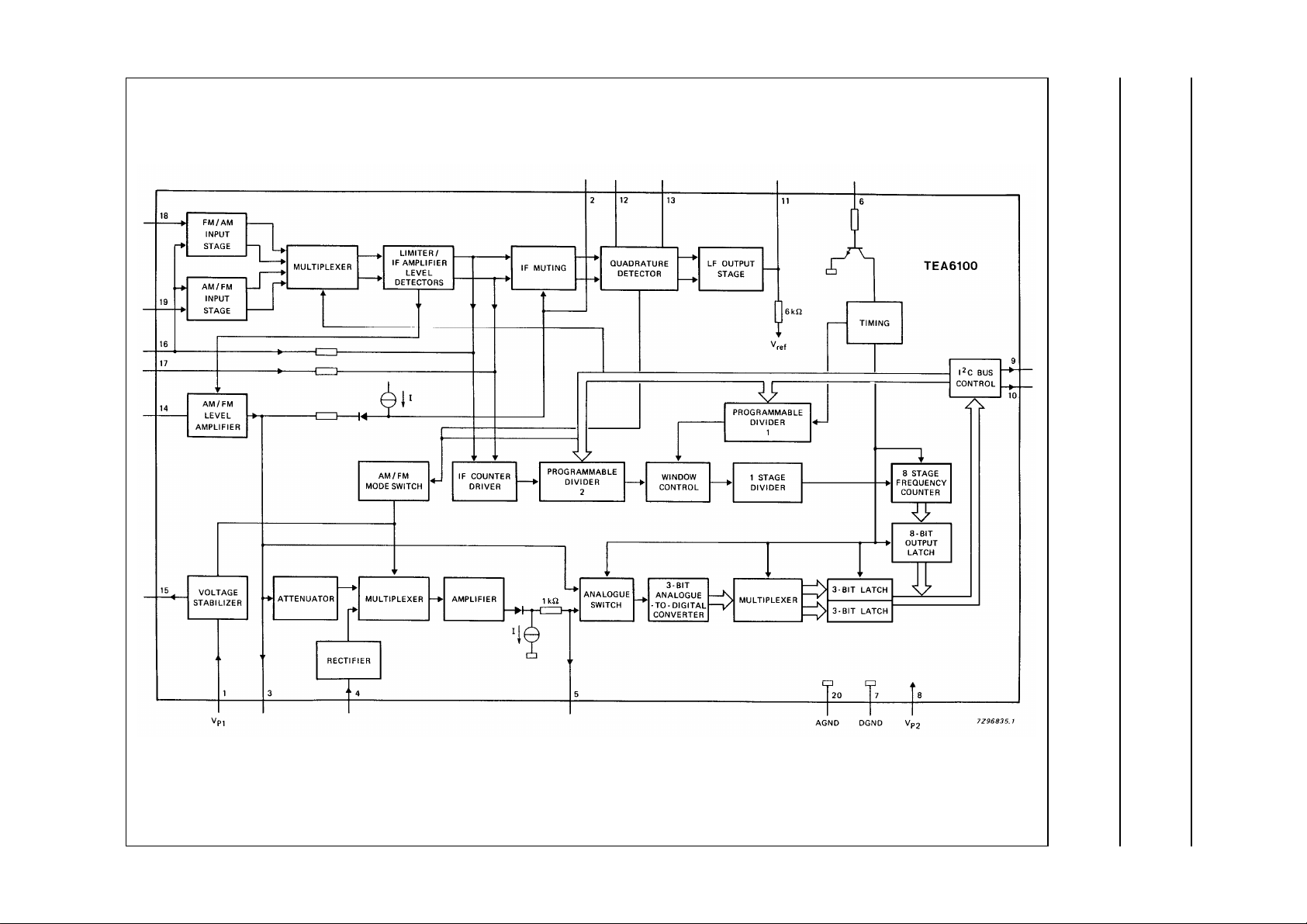
Fig.1 Block diagram.
TEA6100
Page 5
Philips Semiconductors Product specification
FM/IF system and microcomputer-based
tuning interface
PINNING
1V
P1
2 MUTE IN mute input
3 LA OUT level amplifier output
4 RT/A IN rectifier/amplifier input
5 RT/A OUT rectifier/amplifier output
6F
ref
7 DGND digital ground
8V
P2
9 SCL serial clock line; I
10 SDA serial data line; I
11 LF OUT audio output signal
12 Q-DET phase shift for quadrature
13 Q-DET phase shift for quadrature
14 LADJ level amplifier adjustment
15 V
ref
16 FB DEC decoupled feedback
17 FB DEC decoupled feedback
18 INPUT 1 FM/AM IF input
19 INPUT 2 AM/FM IF input
20 AGND analogue ground
analogue supply voltage
reference frequency input
digital supply voltage
2
C bus
2
C bus
detector
detector
reference voltage
TEA6100
Fig.2 Pinning diagram.
FUNCTIONAL DESCRIPTION (see Figs 1 and 16) The IF amplifier consists of four balanced limiting amplifier stages, two separate inputs (AM and FM) and one output.
Software programming (see Table 2; Figs 4 and 5) allows the input signals (AM/FM) to be inserted on either input (pin
18 or 19). The output drives the frequency counter and via the mute stage, drives the quadrature detector. The output of
the quadrature detector is applied to an audio stage (which has a single-ended output). The AM/FM level amplifier, which
is driven by 5 IF level detectors, generates a signal dependent d.c. voltage. The level output voltage is used internally to
control the mute stage and, if required, the signal can be used externally to control the stereo channel separation and
frequency response of a stereo decoder. The signal is also feed to the analogue-to-digital converter (ADC). Due to the
front-end spread in the amplification, the level voltage is made adjustable (LADJ, pin 14). The level voltage amplifier
controls the mute stage and this insures the −3 dB limiting point remains constant, independent of the front-end spread.
AM and FM mode have different front-end circuitry, therefore LADJ must be adjustable for both inputs.
The output voltage of the level amplifier is dependent upon the field strength of the input signal. The multi-path of the FM
signal exists in the AM modulation of the input signal. The following method is used to determine the level information
and the amount of multi-path (as a DC voltage):
• the IF level detector detects the multi-path and feds the signal, via the level amplifiers, to the external bandpass filter
(pin 3) and ADC1
• the signal is then fed to an internal rectifier
• the rectified signal is then fed to an amplifier, so at pin 5 the DC level information is externally available and internally
used by ADC2
In the FM mode, the DC information concerning the multi-path is available at pin 5 and the level information is available
at pin 3.
August 1987 5
Page 6

Philips Semiconductors Product specification
FM/IF system and microcomputer-based
TEA6100
tuning interface
In the AM mode, the level information at pin 3 cannot be directly used owing to AM modulation on the output signal of
the level amplifier. This signal requires filtering, which is achieved by the following method:
• the multiplexer is switched to a position which causes the signal to be applied to the attenuator
• after attenuation the signal is fed to an amplifier (the resultant gain of attenuator and amplifier is unity), after
amplification the signal is filtered by an internal resistor and external capacitor
• after filtering the signal is applied to ADC2 and is externally available
In AM mode pin 5 contains the level information.
The voltages on pin 3 and 5 are converted into two 3-bit digital words by the ADC, which can then be read out by the
I2C bus. The meaning of the 3- bit words is shown in Table 1.
Table 1 3-bit words
WORD
FM AM
1 multipath level without modulation
2 level level with modulation
The FM modulated signal is converted into an audio signal by the symmetrical quadrature detector. The main advantage
of such a detector is that it requires few external components.
POSITION
An FM signal requires good AM suppression, and as a result, the IF amplifiers must act as limiters. To achieve good
suppression on small input signals the IF amplifiers must have a high gain and thus a high sensitivity. High sensitivity is
an undesirable property when used in car radio applications, this problem is solved by having an externally adjustable
mute stage to control the overall sensitivity of the device.
The IF mute stage is controlled by the level amplifier (soft muting) and is only active in FM mode. If the input falls below
a predetermined level, the mute stage becomes active. To avoid the 'ON/OFF' effect of the audio signal due to
fluctuations of the input signal, the mute stage is activated rapidly but de-activated slowly. The mute stage is de-activated
slowly, via a current source and an external capacitor at pin 2, to avoid aggressive behaviour of the audio signal. It is
possible to adjust the '−3 dB limiting point' of the audio output via the level voltage due to the level signal being externally
adjustable. If hard muting is required then pin 2 must be switched to ground.
The 8-bit counter allows accurate stop information to be obtained, because exact tuning is achieved when the measured
frequency is equal to the centre frequency of the IF filter.
To measure the input frequency, the number of pulses which occur in a defined time must be counted. This defined time
is refered to as 'window'. A wide window indicates a long measuring time and therefore a high accuracy. The counter
resolution is defined as Hertz per count. Due to the TEA6100 having to measure the IF frequencies of AM and FM, the
counter resolution must be adjustable (different channel spacing). The counter resolution depends on the setting of
dividers 1 (N1), divider 2 (N2) and the reference frequency (F
software (see section PROGRAMMING INFORMATION). In Table 3 the window and counter resolution has been
calculated for a reference frequency of 40 kHz. The accuracy is controlled by bit 7 of the input word. Although the
resolution is the same for bit 7 = logic 0 and bit 7 = logic 1, the width of the window doubles when bit 7 = logic 1.
• bit 7 = 0, accuracy = ± counter resolution
• bit 7 = 1, accuracy = ± 1⁄2 counter resolution
). The divider ratios of N1 and N2 are controlled by
ref
August 1987 6
Page 7
Philips Semiconductors Product specification
FM/IF system and microcomputer-based
TEA6100
tuning interface
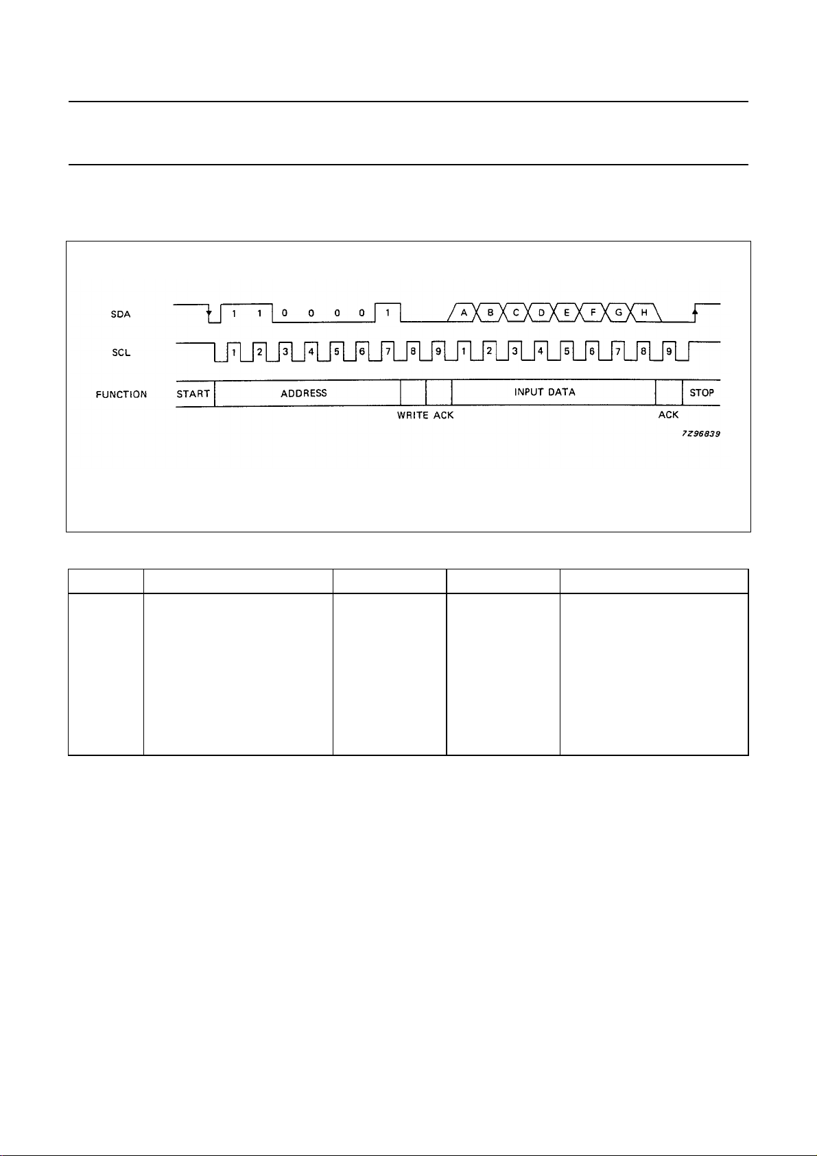
Communication between TEA6100 and the microcomputer is via a two wire bidirectional I2C bus. The power supply lines
are fully isolated to avoid cross talk between the digital and analogue parts of the circuit.
Fig.3 Input data format waveforms.
Table 2 Input bits
BIT FUNCTION LOGIC 0 LOGIC 1 SEE Fig.5 AND 6
1 reference frequency 32 kHz 40 kHz A
2 IF mode AM FM B
3 IF input pin 19 pin 18 C
4 counter input 460 kHz 10,7 MHz D
5 counter mode AM FM E
6 resolution divide by 8 divide by 1 F
7 accuracy LOW HIGH G
8 test mode OFF ON H
August 1987 7
Page 8
This text is here in white to force landscape pages to be rotated correctly when browsing through the pdf in the Acrobat reader.This text is here in
_white to force landscape pages to be rotated correctly when browsing through the pdf in the Acrobat reader.This text is here inThis text is here in
white to force landscape pages to be rotated correctly when browsing through the pdf in the Acrobat reader. white to force landscape pages to be ...
August 1987 8
Philips Semiconductors Product specification
FM/IF system and microcomputer-based
tuning interface
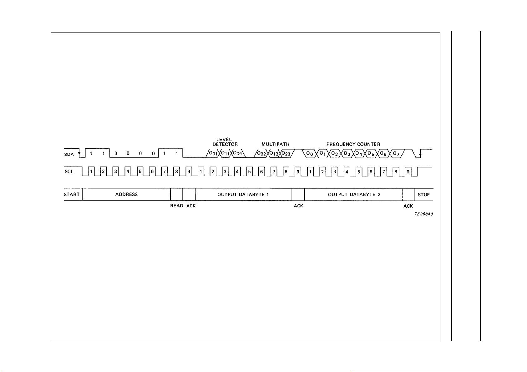
Fig.4 Output data format waveforms.
TEA6100
Page 9
Philips Semiconductors Product specification
FM/IF system and microcomputer-based
tuning interface
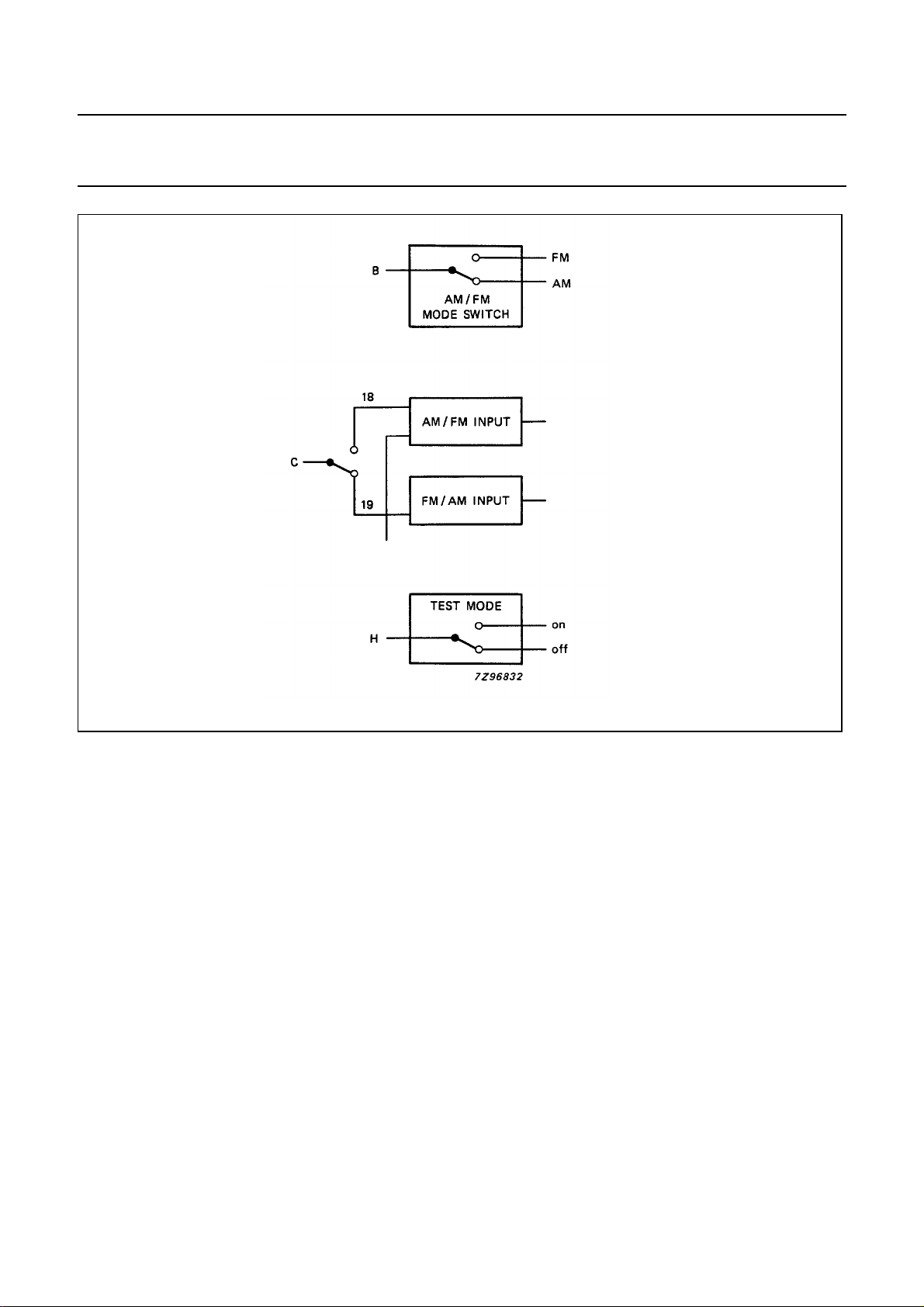
TEA6100
Fig.5 Switch positions, analogue part (switches drawn in logic 0 state).
August 1987 9
Page 10

This text is here in white to force landscape pages to be rotated correctly when browsing through the pdf in the Acrobat reader.This text is here in
_white to force landscape pages to be rotated correctly when browsing through the pdf in the Acrobat reader.This text is here inThis text is here in
white to force landscape pages to be rotated correctly when browsing through the pdf in the Acrobat reader. white to force landscape pages to be ...
August 1987 10
Philips Semiconductors Product specification
FM/IF system and microcomputer-based
tuning interface
Fig.6 Switch positions, digital part (switches drawn in logic 0 state, see Tables 2 and 3).
TEA6100
Page 11

Philips Semiconductors Product specification
FM/IF system and microcomputer-based
TEA6100
tuning interface
Table 3 Possible window settings and counter resolutions with a 40 kHz reference frequency (see Figs 5 and 6)
POSITION OF
SWITCH
ADEFG
00000 25,6 39,1 460,0 4F 456,914 466,875
10000 32,0 31,3 460,0 CF 453,531 461,500
00001 51,2 39,1 460,0 4F 456,914 466,875
10001 64,0 31,3 460,0 CF 453,531 461,500
00100 128,0 1000,0 460,0 C3 265,000 520,000
10100 160,0 800,0 460,0 36 416,800 620,800
00101 256,0 1000,0 460,0 C3 256,000 520,000
10101 320,0 800,0 460,0 36 416,800 620,800
00010 3,2 312,5 460,0 0F 455,312 535,000
10010 4,0 250,0 460,0 7F 428,250 492,000
00011 6,1 312,5 460,0 0F 455,312 535,000
10011 8,0 250,0 460,0 7F 428,250 492,000
00110 16,0 8000,0 460,0 30 76,000 2116,000
10110 20,0 6400,0 460,0 3F 56,800 1688,800
00111 32,0 8000,0 460,0 30 76,800 2116,000
10111 40,0 6400,0 460,0 3F 56,800 1688,800
01000 25,6 625,0 10700,0 2F 10670,625 10830,000
11000 32,0 500,0 10700,0 E7 10584,500 10712,000
01001 51,2 625,0 10700,0 2F 10670,625 10830,000
11001 64,0 500,0 10700,0 E7 10584,000 10712,000
01100 128,0 1000,0 10700,0 C3 10505,000 10760,000
11100 160,0 800,0 10700,0 36 10656,800 10860,800
01101 256,0 1000,0 10700,0 C3 10505,000 10760,000
11101 320,0 800,0 10700,0 36 10656,800 10860,000
01010 3,2 5000,0 10700,0 AB 9845,000 11120,000
11010 4,0 4000,0 10700,0 C2 9924,000 10944,000
01011 6,4 5000,0 10700,0 AB 9845,000 11120,000
11011 8,0 4000,0 10700,0 C2 9924,000 10944,000
01110 16,0 8000,0 10700,0 30 10316,000 12356,000
11110 20,0 6400,0 10700,0 7F 9887,200 11519,200
01111 32,0 8000,0 10700,0 30 10316,000 12356,000
11111 40,0 6400,0 10700,0 7F 9887,200 11519,200
WINDOW (ms)
COUNTER
RESOLUTION
Hz / COUNT
IF
FREQUENCY
(kHz)
READ OUT BY
IF FREQUENCY
(HEX)
RANGE (kHz)
MIN. MAX.
August 1987 11
Page 12

Philips Semiconductors Product specification
FM/IF system and microcomputer-based
tuning interface
RATINGS
Limiting values in accordance with the Absolute Maximum System (IEC 134)
PARAMETER CONDITIONS SYMBOL MIN. MAX. UNIT
Supply voltage pins 1 and 8 V
Total power dissipation P
Storage temperature range T
Operating ambient temperature range T
THERMAL RESISTANCE
From junction to ambient R
P1
tot
stg
amb
, V
P2
0 13,2 V
see Fig.7
−65 +150 °C
−30 +85 °C
th j-a
TEA6100
70 K/W
Fig.7 Power derating curve.
DC CHARACTERISTICS (note)
= VP2 = 8,5 V; T
V
P1
= 25°C; all currents positive into the IC; unless otherwise specified
amb
PARAMETER CONDITIONS SYMBOL MIN. TYP. MAX. UNIT
Supply voltage pins 1 and 8 V
Supply current
FM mode V
AM mode V
> 2,4 V I
ADJ
> 2,4 V I
ADJ
digital part I
Power dissipation P
August 1987 12
P1
P1
P2
P1
d
, V
P2
7,5 8,5 12 V
− 19 25 mA
− 15 25 mA
− 16 23 mA
− 280 − mW
Page 13

Philips Semiconductors Product specification
FM/IF system and microcomputer-based
TEA6100
tuning interface
AC CHARACTERISTICS (note 1) V
= 8,5 V; V
P
PARAMETER CONDITIONS SYMBOL MIN. TYP. MAX. UNIT
IF amplifier, quadrature
detector and LF amplifier
output
Sensitivity −3 dB before limiting;
Sensitivity S/N = 26 dB;
Signal plus noise V
to noise ratio bandwidth = 0,3 to
IF input range AM suppression
Audio output
voltage after
limiting ∆f = 22,5 kHz V
Total harmonic
distortion for
single tuned
circuit ∆f = 75 kHz THD − 0,65 − %
AM suppression note 2; see Figs 8, 9 and 10;
Supply voltage
ripple rejection 200 Hz; 20 log (V
IF counter inputs
Frequency counter minimum input voltage
sensitivity for a readout ±1 bit;
FM mode 10,7 MHz V
AM mode 10,7 MHz V
AM mode 460 kHz V
Maximum input
voltage V
= 1 mV; f = 10,7 MHz; ∆f = 22,5 kHz; fm = 1 kHz; FM mode; unless otherwise specified
i(FM)
pin 11
inactive mute V
inactive mute V
= 10 mV;
i(FM)
i(FM)
i(FM)
− 15 30 µV
− 12 −µV
15 kHz;
∆f = 75 kHz (S + N)/N − 85 − dB
> 40 db V
i(FM)
− 0,09 to
1000
160 200 240 mV
V
range = 200 µV
i(AM)
o
to 600 mV AMS − 60 − dB
V
range = 200 µV
i(AM)
to 600 µV AMS − 55 − dB
/ Vo) SVRR 38 40 − dB
i
i(FM)
i(AM)
i(AM)
i
−−60 µV
−−60 µV
−−45 µV
−−1V
− mV
August 1987 13
Page 14

Philips Semiconductors Product specification
FM/IF system and microcomputer-based
tuning interface
PARAMETER CONDITIONS SYMBOL MIN. TYP. MAX. UNIT
FM level performance
Output voltage
adjustment range V
Maximum output
voltage pins 3 and 14 V
Adjustable gain V
Level voltage slope V
Output impedance
of level amplifier V
AM level
performance
Output voltage
adjustment range V
Adjustable gain V
Level voltage slope V
IF soft muting
Mute operating
range V
Mute voltage −3 dB output
Maximum muting V
IF hard muting
Mute voltage −60 dB output
Mute discharge
current V
Mute charging V
current mute OFF −I
see Fig.11
= 0 V;
i(FM)
pins 3 and 14 V
i(FM)/VADJ
= 2,4 V;
ADJ
V
= 100 to 10 mV S
i(FM)
> 1 V |Zo| − 100 −Ω
LFM
see Fig.12
= 0 V;
i(AM)
pins 5 and 14 V
V
= 10 mV;
i(AM)
pins 5 and 14 V
/ V
V
V
i(AM)
ADJ
i(FM)
LFM
ADJ
= 2,4 V;
= 100 to 10 mV S
; pin 3;
see Fig.13
attenuation V
= 0,1 V V
LFM
V
; pin 2
MUTE
attenuation V
= 1 V;
MUTE
V
LEVEL
= 0 V;
mute ON; pin 2 +I
= 0 V;
MUTE
LFM
LFM
G
i(FM)
LFM
LAM
G
i(AM)
LFM
LFM
MUTE
MUTE
ADJ
ADJ
2
2
TEA6100
− 0,1 to 4,6 − V
VP−1,5 −−V
−−2−dB
1,4 1,6 1,8 V/dec
− 0,1 to 4,6 − V
6 −−V
−−2−dB
1,3 1,5 1,7 V/dec
− 0,1 to 2,5 − V
1,20 1,45 1,75 V
− 19 − dB
− 460 − mV
− 270 −µA
− 1,5 −µA
(6)
(6)
August 1987 14
Page 15

Philips Semiconductors Product specification
FM/IF system and microcomputer-based
tuning interface
PARAMETER CONDITIONS SYMBOL MIN. TYP. MAX. UNIT
Rectifier/amplifier
Input impedance pin 4 |Z
Conversion gain pins 4 and 5;
AC to DC bandwith = 100 Hz to
120 kHz;
20 log V
V
(a.c.) G
i(MP)
DC output voltage
range V
Output characteristics
see Fig.16; note 3
Discharge current I
Output ripple in f
AM mode (peak- V
= 200 Hz; m = 0,8;
m
range = 100 µV
i(AM)
to-peak value) to 30 mV V
Multi-path output
Reference voltage
see Figs 14 and 15; note 4
pin 15, FM only
output
Output voltage V
Output sink current +I
Output impedance |Z
Output charge
current −I
Output voltage AM mode V
Output impedance AM mode |Z
2
C bus data format
I
see Fig.3 and 4;
Table 2
3-bit ADC
multi-path and level
information, note 5
Trip level LOW V
Trip level HIGH V
Reference
pin 6
frequency input
Reference range F
Input voltage LOW V
Input current HIGH I
O(MP)
(d.c.)/
TEA6100
| 7 10 13 kΩ
i
A
O(MP)
o
ripple
ref
15
| −−10 Ω
O
15
ref
| − 14 − kΩ
O
TL
TH
ref
IL
IH
− 30 − dB
− 0,2 to 6 − V
− 200 −µA
− 300 400 mV
− 4,4 − V
−−1,5 mA
5 −−mA
− 0 − V
1,20 1,45 1,75 V
4,25 4,50 4,75 V
−−40 kHz
−−0,4 V
5 −−µA
August 1987 15
Page 16

Philips Semiconductors Product specification
FM/IF system and microcomputer-based
tuning interface
Notes
1. All characteristics are measured from the circuit shown in Fig.16.
2. Conditions for this parameter are:
20 log V
3. Voltage source followed by diode and resistor.
4. A DC shift can be achieved by connecting a 1,8 MΩ resistor between pin 4 and pin 15.
5. Step size between trip levels:
(VTH− VTL) / 6 ± 0,07 V.
6. V/dec = voltage per decade.
; m = 0,3 or 20 log V
o(FM)
o(AM)
; m = 0,3.
TEA6100
August 1987 16
Page 17

Philips Semiconductors Product specification
FM/IF system and microcomputer-based
tuning interface
(1) Audio (∆f = 22,5 kHz and f
(2) Noise (with dBA filter) for V
(3) AM suppression (m = 0,3 and f
= 1 kHz) for V
mod
= 0 V.
ADJ
= 1 kHz) for V
mod
ADJ
= 0 V.
ADJ
= 0 V.
TEA6100
Fig.8 Audio output voltage performance plotted against input signal, V
(1) Audio (∆f = 22,5 kHz and f
(2) Noise (with dBA filter) for V
= 1 kHz) for V
mod
= 2,4 V.
ADJ
ADJ
= 2,4 V.
i(FM)
.
Fig.9 Audio output voltage performance plotted against input signal, V
August 1987 17
i(FM)
.
Page 18

Philips Semiconductors Product specification
FM/IF system and microcomputer-based
tuning interface
TEA6100
(1) V
(2) V
(3) V
ADJ
ADJ
ADJ
= 1,4 V.
= 2,4 V.
= 3,4 V.
Fig.10 Total harmonic distortion; ∆f = 75 kHz, f
= 1 kHz and V
mod
ADJ
= O V.
Fig.11 Level voltage output (V
) plotted against IF input signal, V
LFM
August 1987 18
; IF = 10,7 MHz.
i(FM)
Page 19

Philips Semiconductors Product specification
FM/IF system and microcomputer-based
tuning interface
(1) V
= 1,4 V.
ADJ
(2) V
= 2,4 V.
ADJ
(3) V
= 3,4 V.
ADJ
TEA6100
Fig.12 Level voltage output (V
) plotted against IF input signal, V
LAM
; IF = 10,7 MHz or 460 kHz.
i(AM)
Fig.13 Soft muting plotted against level output voltage; V
August 1987 19
= 1 mV and ∆f = 22,5 kHz.
i(FM)
Page 20

Philips Semiconductors Product specification
FM/IF system and microcomputer-based
tuning interface
(1) mod = 0,2
(2) mod = 0,3
(3) mod = 0,4
TEA6100
Fig.14 Multi-path output plotted against IF input signal, V
and 1,8 MΩ resistor connected between pin 4 and pin 15.
(1) mod = 0,2
(2) mod = 0,3
(3) mod = 0,4
i(FM)
; f
= 3 kHz (AM, no FM modulation), V
mod
ADJ
= 2,4 V
Fig.15 Multi-path output plotted against IF input signal, V
August 1987 20
i(FM)
; f
= 3 kHz (AM, no FM modulation), V
mod
ADJ
= 2,4 V.
Page 21

Philips Semiconductors Product specification
FM/IF system and microcomputer-based
tuning interface
APPLICATION INFORMATION
TEA6100
Fig.16 Application diagram.
August 1987 21
Page 22

Philips Semiconductors Product specification
FM/IF system and microcomputer-based
tuning interface
TEA6100
Fig.17 Track side of printed circuit board.
Fig.18 Component side of printed circuit board.
August 1987 22
Page 23

Philips Semiconductors Product specification
FM/IF system and microcomputer-based
tuning interface
Double tuned circuit
TEA6100
R1 = 5,1 kΩ, R2 = 1,5 kΩ
C1 = C2 = 150 pF (n = 220)
C3 = C4 = 10 pF
L1 = L2 = 1,6 µH
Fig.19 Double tuned demodulator circuit.
Alignment of the circuit is obtained with an IF input signal > 200 µV. Tuning the circuit is performed by, detuning L2,
adjusting L1 to obtain a minimum distortion level and then adjusting L2 to obtain a minimum distortion level.
Fig.20 Total harmonic distortion plotted against IF detuning; for ∆f = ± 75 kHz, f
August 1987 23
= 1 kHz and VO = 500 mV.
mod
Page 24

Philips Semiconductors Product specification
FM/IF system and microcomputer-based
TEA6100
tuning interface
PROGRAMMING INFORMATION
Converting the read out of the counters into frequency
The counter resolution at the input is defined as:
• resolution = divider ratio of N2/window
For every increment of the counter the counted frequency increases relative to the resolution in Hertz, as shown in
example:
• window = 20 ms; N2 = 128; IF frequency = 10,7 MHz; resolution = 128/0,02 = 6,4 kHz per count
The counter consists of 8 bits. Therefore, the maximum frequency range that can be counted is
256 × resolution = 1,6384 MHz. In the example the frequency to be counted is 10,7 MHz, therefore, the counter will
overflow (in the example above, 7 times). The real measured frequency is:
• f
= (read out + overflow × 256) × resolution
real
The overflow indicates the off-set on the frequency scale which must be added to the read out. Due to the bandwidth of
the IF filter, the frequencies at the input to the TEA6100 are known, for example:
• IF filter for FM has a center frequency of 10,7 MHz and −3 dB bandwidth of 300 kHz. Only the frequencies of 10,7 MHz
± 150 kHz occur at the input of the TEA6100. For this reason it is not necessary to count the overflow.
The read out of the counter has to be translated into frequency. This translation depends upon the counter resolution.
The preferred way to calculate the input frequency is to:
• calculate the read out of the target IF frequency. Compare this value with that of the measured read out and multiply
the difference by the resolution.
The formulae for calculating the target IF read out and the resolution are as follows (A, D, E, F and G refer to the bits of
the I2C bus input data as shown in Fig.3 and 4 and to the counter/timer block diagram shown in Fig.6. An, Dn, En, Fn
and Gn are inverted values of the variables A, D, E, F and G. Table 3 shows the following formulae calculated for a
reference frequency of 40 kHz):
• N1 = (An × 4 + A × 5) × (En × 4 + E × 5) × 8 × (2
• Window (T) = N1/F
• N2 = (E × 16 × 8 + En × [Dn × 1 +D × 16]) × (G × 2 + Gn × 1)
• Target decimal read out (TDEC) = T × (TIFF/N2 + (E × 247 + En × 79). TIFF is the symbol for target IF frequency
• Target read out hexadecimal (THEX), convert the target decimal read out to hexadecimal and use the 2 least
significant digits (Do not use overflow value). The symbol for measured hexadecimal is MHEX
• Resolution (R) = N2/T
• Measured frequency (FI) = (TIFF) + R × (MHEX − THEX).
Note
Care should be taken if TIFF +
or if TIFF −1⁄2 filter bandwith is less than the frequency at read out for hexadecimal value 00.
• Counter accuracy (AW and AN), with bit 7 (G) the accuracy can be chosen with the same resolution. If bit 7 is logic 1
the accuracy is HIGH and if bit 7 is logic 0 then the accuracy is LOW.
bit 7 = 0, AN = ± (N2/T)
bit 7 = 1, AW = ± (1⁄2× N2/T)
ref
1
⁄2 filter bandwidth is greater than the frequency for the read out of hexadecimal value FF,
[E × 2+G × 1]
) × (F × 1 + Fn × 8)
August 1987 24
Page 25

Philips Semiconductors Product specification
FM/IF system and microcomputer-based
tuning interface
Example
The example uses the following values:
TIFF = 10,7 MHz; accuracy = LOW (G = 0); F
resolution = N1 (F = 1) and counter mode = FM (E = 1)
N1 = (0 × 4 + 1 × 5) × (0 × 4 + 1 × 5) × 8 × (2
T = 800/40 = 20 ms
N2 = (1 × 16 × 8 + 0 × [1 × 1 + 0 × 16]) × (0 × 2 + 1 × 1) = 128
TDEC = 20 × 10,7/128 + (1 × 247 + 0 × 79) = 1919
THEX; 1919 is hexadecimal 77F and the least significant 2 digits are 7F, so THEX = 7 F
R = 128/20 = 6400 Hz/count
Assume the readout is '6E', the measured frequency will be:
= 10,7 + (6E − 7F) × 6400 = 10,59 MHz
• F
I
Assume the readout is '83', the measured frequency will be:
• FI = 10,7 + (83 − 7F) × 6400 = 10,726
= 40 kHz (A = 1); IF frequency = 10, 7 MHz (D = 1);
ref
[1 × 2 + 0 × 1]
) × (1 × 1 + 0 × 8) = 800
TEA6100
August 1987 25
Page 26

Philips Semiconductors Product specification
FM/IF system and microcomputer-based
tuning interface
PACKAGE OUTLINE
DIP20: plastic dual in-line package; 20 leads (300 mil)
D
seating plane
L
Z
20
e
b
TEA6100
SOT146-1
M
E
A
2
A
A
1
w M
b
1
11
c
(e )
1
M
H
pin 1 index
1
0 5 10 mm
scale
DIMENSIONS (inch dimensions are derived from the original mm dimensions)
A
A
A
UNIT
inches
Note
1. Plastic or metal protrusions of 0.25 mm maximum per side are not included.
max.
mm
OUTLINE
VERSION
SOT146-1
1 2
min.
max.
1.73
1.30
0.068
0.051
IEC JEDEC EIAJ
b
b
1
0.53
0.38
0.021
0.015
0.36
0.23
0.014
0.009
REFERENCES
cD E e M
(1) (1)
26.92
26.54
1.060
1.045
SC603
6.40
6.22
0.25
0.24
E
10
(1)
M
e
L
1
3.60
8.25
3.05
7.80
0.14
0.32
0.12
0.31
EUROPEAN
PROJECTION
H
E
10.0
0.2542.54 7.62
8.3
0.39
0.010.10 0.30
0.33
ISSUE DATE
w
92-11-17
95-05-24
Z
max.
2.04.2 0.51 3.2
0.0780.17 0.020 0.13
August 1987 26
Page 27

Philips Semiconductors Product specification
FM/IF system and microcomputer-based
tuning interface
SOLDERING
Introduction
There is no soldering method that is ideal for all IC
packages. Wave soldering is often preferred when
through-hole and surface mounted components are mixed
on one printed-circuit board. However, wave soldering is
not always suitable for surface mounted ICs, or for
printed-circuits with high population densities. In these
situations reflow soldering is often used.
This text gives a very brief insight to a complex technology.
A more in-depth account of soldering ICs can be found in
our
“IC Package Databook”
Soldering by dipping or by wave
The maximum permissible temperature of the solder is
260 °C; solder at this temperature must not be in contact
DEFINITIONS
(order code 9398 652 90011).
TEA6100
with the joint for more than 5 seconds. The total contact
time of successive solder waves must not exceed
5 seconds.
The device may be mounted up to the seating plane, but
the temperature of the plastic body must not exceed the
specified maximum storage temperature (T
printed-circuit board has been pre-heated, forced cooling
may be necessary immediately after soldering to keep the
temperature within the permissible limit.
Repairing soldered joints
Apply a low voltage soldering iron (less than 24 V) to the
lead(s) of the package, below the seating plane or not
more than 2 mm above it. If the temperature of the
soldering iron bit is less than 300 °C it may remain in
contact for up to 10 seconds. If the bit temperature is
between 300 and 400 °C, contact may be up to 5 seconds.
stg max
). If the
Data sheet status
Objective specification This data sheet contains target or goal specifications for product development.
Preliminary specification This data sheet contains preliminary data; supplementary data may be published later.
Product specification This data sheet contains final product specifications.
Limiting values
Limiting values given are in accordance with the Absolute Maximum Rating System (IEC 134). Stress above one or
more of the limiting values may cause permanent damage to the device. These are stress ratings only and operation
of the device at these or at any other conditions above those given in the Characteristics sections of the specification
is not implied. Exposure to limiting values for extended periods may affect device reliability.
Application information
Where application information is given, it is advisory and does not form part of the specification.
LIFE SUPPORT APPLICATIONS
These products are not designed for use in life support appliances, devices, or systems where malfunction of these
products can reasonably be expected to result in personal injury. Philips customers using or selling these products for
use in such applications do so at their own risk and agree to fully indemnify Philips for any damages resulting from such
improper use or sale.
2
PURCHASE OF PHILIPS I
C COMPONENTS
Purchase of Philips I
components in the I2C system provided the system conforms to the I2C specification defined by
Philips. This specification can be ordered using the code 9398 393 40011.
August 1987 27
2
C components conveys a license under the Philips’ I2C patent to use the
 Loading...