

Page 1
.
1 VIDEO OUTPUT 75Ω-1V
SWITCHED
.
1 SWITCHEDVIDEOOUTPUT 2V
.
VIDEOCROSSTALK : 50dB TYPICAL
.
SHORT CIRCUIT PROTECTION OF INPUTS
ANDOUTPUTS
.
CLAMPEDVIDEO INPUTS
PP
PP
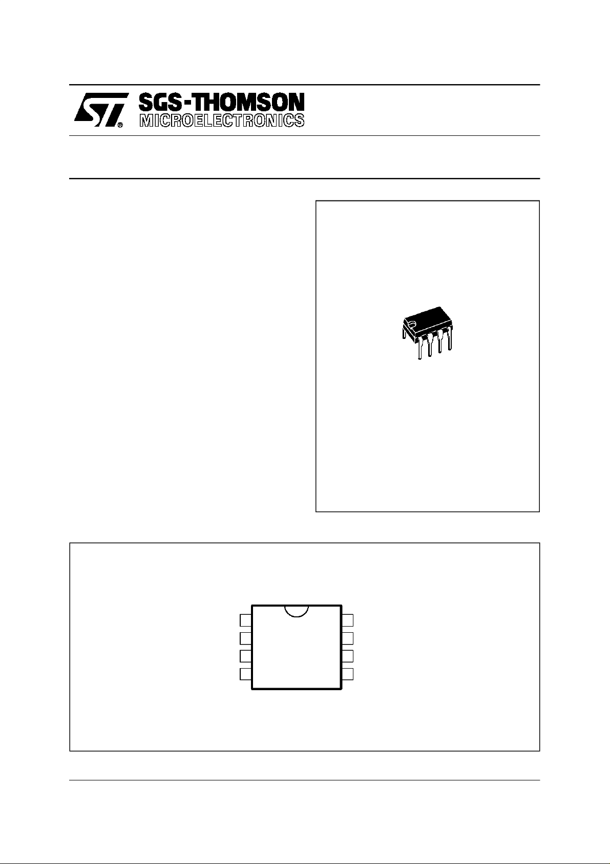
TEA2014A
VIDEO SWITCH
NOT
DIP8
(Plastic package)
ORDER CODE : TEA2014A
DESCRIPTION
This integrated circuit providesall video switching
allowingconnectionsbetweentheperi TV plugand
video sections in the TV set. The TEA2014A is
suppliedin a DIP8.
PINCONNECTIONS
GROUND
75ΩVIDEO OUTPUT
INTERNAL VIDEO INPUT
NOT TO BE USED
1
2
3
4
8
EXTERNAL VIDEO INPUT
7
SUPPLY VOLTAGE
6
SWITCHED VIDEO OUTPUT
5
SWITCHING INPUT
2014A-01.EPS
May 1996
1/4
Page 2

TEA2014A
ABSOLUTE MAXIMUM RATINGS
Symbol Parameter Value Unit
V
CC
T
oper
T
T
stg
– Minimum DC Load Resistor PIN6
THERMALDATA
Symbol Parameter Value Unit
R
th (j-a)
ELECTRICAL CHARACTERISTICS
=+25°C, VCC= 9 V (unless otherwisespecified)
T
amb
Symbol Parameter Min. Typ. Max. Unit
V
CC
I
CC
I
CC
P
tot
INPUTS (pin8 and pin3)
– Internal Video Input Swing from Picture IF (positive Video) – – 4.5 Vpp
– Internal Video Input Impedance (positivevideo) 50 – – kΩ
– Internal Video Input Bias Current (positive video) 6 25 40 µA
– External Video Input Swing (positivevideo) – – 2 Vpp
– External Video Input Impedance (positive video) 50 – – kΩ
SWITCHED OUTPUT (pin 6) - R
– VideoOutput Swing 4 – – Vpp
– VideoOutput Dynamic Impedance – – 25 Ω
– VideoDC Output Voltage (sync. pulselevel note 1) 1.7 2 2.4 V
– VideoBandwith Pin 6 – from Internal Input Pin3 (– 1 dB) 6 – – MHz
– VideoBandwith Pin 6 – from External Input Pin 8 (– 3 dB) 6 – – MHz
– Output Gain Pin 6 – Pin 8 +5 +6 + 7 dB
– Output Gain Pin 6 – Pin 3 – 1 – 0.5 0 dB
EXTERNAL OUTPUT (pin2) - R
– VideoOutput Swing 2.2 – – Vpp
– VideoOutput Dynamic Impedance – 10 – Ω
– VideoDC Output Voltage (sync. pulselevel , note) 1.7 2 2.4 V
– VideoBandwidth (– 1dB) 6 – – MHz
– VideoOutput Gain (pin2 – pin 3) – 1.8 – 1 – 0.4 dB
SWITCHING INPUT (pin 5)
– SwitchingInput Unactive Low Level or Unconnected Pin(TV receiving) 0 – 3 V
– SwitchingInput Active Level (ext. receiving) 7 – V
– SwitchingInput Impedance 10 – – kΩ
Note : Use a video signal witha synchro pulse in order to make the clamp work in acorrect way.
(75Ω to the ground and 10µF in series).
Supply Voltage 18 V
Operating Temperature
with Load > 150 Ω onPIN 2
with Load = 75 Ω on PIN2
Junction Temperature – 40, + 150 °C
j
0, + 100
0, + 70
Storage Temperature – 40, + 150 °C
600
Minimum DC Load Resistor PIN2
75
Junction-ambient Thermal Resistance Typ. 90 °C/W
Supply Voltage Range 8 – 14 V
Supply Current (no loadon Pin 2 and Pin 6) – – 20 mA
Supply Current (with 75 Ω Pin 2.1, with 600 Ω betweenPin 6.1) – 45 – mA
Total Power Dissipation with Load – 400 – mW
= 600 Ω
LOAD
=75Ω
LOAD
CC
°C
Ω
Ω
2014A-01.TBL
2014A-02.TBL
V
2014A-03.TBL
2/4
Page 3

TEA2014A
ELECTRICAL CHARACTERISTICS (continued)
=+25°C, VCC= 9 V (unless otherwisespecified)
T
amb
Symbol Parameter Min. Typ. Max. Unit
OTHER DYNAMIC FEATURES
– Videorejection Between Two Inputs
– LinearityDistortion
Luma (test line 17)
Chroma (test line 331)
Intermodulation Luma – Chroma (testline 331)
– SupplyVoltage Rejection(1 kHz) 40 50 – dB
TYPICALAPPLICATION
External
Video Input
1MHz
1kHz
–
–50–––dB
–50
–
2
–
–
V
CC
O or no connected = Video TV
–
2
–
5
–
Switching Input
7V = External Video
10kΩ
7
5
G=2
8
dB
%
%
%
2014A-04.TBL
Reference
(low impedance)
Video coming
from TV 2Vpp
3
2mA
G=1
TEA2014A
75Ω
We advice to protect the 75 Ω output through a 75 Ω resistor for supply voltage higher than 9 V.
Video
1Vpp
75
Ω
6
600
Video
2Vpp
Ω
12
2014A-02.EPS
3/4
Page 4

TEA2014A
PACKAGEMECHANICALDATA
8 PINS– PLASTICDIP
Dimensions
Min. Typ. Max. Min. Typ. Max.
Millimeters Inches
A 3.32 0.131
a1 0.51 0.020
B 1.15 1.65 0.045 0.065
b 0.356 0.55 0.014 0.022
b1 0.204 0.304 0.008 0.012
D 10.92 0.430
E 7.95 9.75 0.313 0.384
e 2.54 0.100
e3 7.62 0.300
e4 7.62 0.300
F 6.6 0260
I 5.08 0.200
L 3.18 3.81 0.125 0.150
Z 1.52 0.060
Information furnishedis believed to be accurate and reliable. However, SGS-THOMSON Microelectronicsassumes no responsibility
for the consequences of use of such information norfor any infringement of patents or otherrights of third parties which may result
from its use. Nolicence is granted by implication or otherwise under any patent or patent rights of SGS-THOMSON Microelectronics.
Specifications mentioned in this publication are subject to change without notice. This publication supersedes and replaces all
information previouslysupplied. SGS-THOMSON Microelectronics products are not authorized for use as critical components in life
support devices or systems without express written approval of SGS-THOMSON Microelectronics.
1996 SGS-THOMSON Microelectronics - All Rights Reserved
Purchase of I
2
I
C Patent. Rights to use these components in a I2C system, is granted provided that the system conformsto
Australia - Brazil -Canada - China - France - Germany - Hong Kong - Italy -Japan - Korea - Malaysia - Malta - Morocco
The Netherlands - Singapore - Spain - Sweden - Switzerland - Taiwan - Thailand - United Kingdom -U.S.A.
2
C Components of SGS-THOMSON Microelectronics, conveys a license under the Philips
2
the I
C Standard Specifications as defined by Philips.
SGS-THOMSON Microelectronics GROUP OF COMPANIES
PM-DIP8.EPS
DIP8.TBL
4/4
 Loading...