

Page 1

查询TEA1566供应商
INTEGRATED CIRCUITS
DATA SH EET
TEA1566
GreenChip; SMPS module
Preliminary specification
File under Integrated Circuits, IC11
1999 Apr 20
Page 2
Philips Semiconductors Preliminary specification
GreenChip; SMPS module TEA1566
FEATURES
Distinctive features
• High level of integration results in 20 to 50 fewer
components compared to a power supply with discrete
components
• On-chip 600 V MOSFET
• On/off function replaces expensive mains switch with
functional switch
• Direct off-line operation (90 to 276 VAC)
• On-chip 5% accurate oscillator.
Green features
• Low power consumption in off-mode (<100 mW)
• On-chip efficient start-up current source giving fast
start-up
• Burst mode stand-by (<2 W) for overall improved
system efficiency
• Low power operation mode with lower frequency to
reduce switching losses.
Protection features
APPLICATIONS
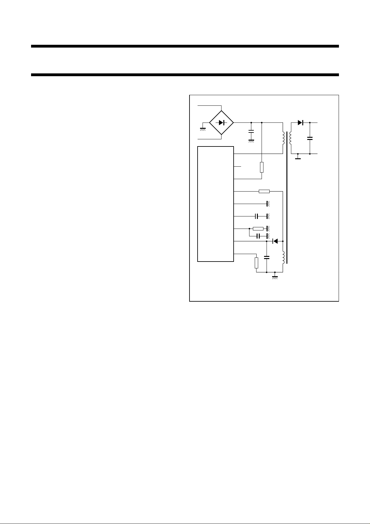
mains
TEA1566
9
8
7
6
5
4
3
2
1
output
Vin
NC
OOB
Dem
Gnd
Vctrl
Iref
Vaux
Isense
• Demagnetization protection
• Cycle by cycle current limitation with programmable
current trip level
• Over voltage protection
• Over temperature protection
• Safe-restart mode with reduced power for system fault
conditions.
Highly versatile
• Usable in Buck and flyback topology
• Interfaces both primary and secondary side feedback.
MGR691
Fig.1 Typical flyback application.
GENERAL DESCRIPTION
The GreenChip, intended for off-line 90 to 276 VAC
power supply applications, is a monolithic high voltage
family of ICs that combines analog and digital circuits to
implement all necessary control functions for a switched
mode power supply. The functions include integrated high
voltage start-up current source, voltage mode PWM
control, 5% accurate trimmed oscillator, band gap derived
reference voltages, comprehensive fault protection, and
leading edge blanking. High level of integration leads to
cost effective power supplies that are compact, weigh less,
and at the same time give higher efficiency, are more
reliable and simple to design. Efficient green features lead
to very low power operation modes and a novel on/off
function helps replace the expensive mains switch with a
low cost functional switch.
1999 Apr 20 2
Page 3
Philips Semiconductors Preliminary specification
GreenChip; SMPS module TEA1566
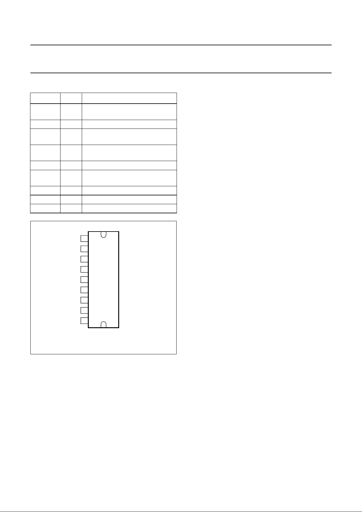
ORDERING INFORMATION
TYPE NUMBER
PACKAGE
NAME DESCRIPTION VERSION
TEA1566S SIL9P plastic single in-line power package; 9 leads SOT131-2
TEA1566J DBS9P plastic DIL-bent-SIL power package; 9 leads (lead length12 mm) SOT157-2
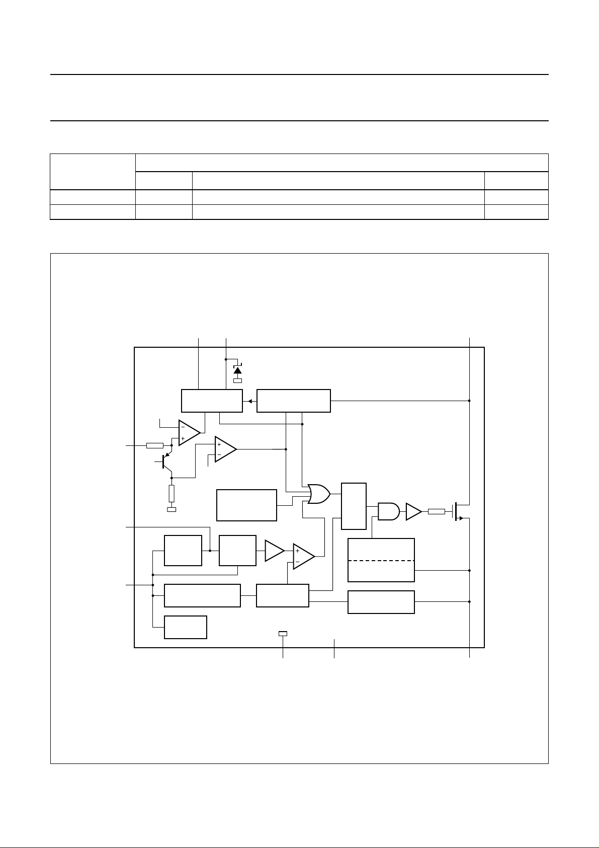
BLOCK DIAGRAM
handbook, full pagewidth
OOB
Vaux
VAUX
ON/OFF
1 kΩ
7
MANAGEMENT
CURRENT SOURCE
START-UP
TEA1566
VinIref
923
Vctrl
Dem
4
6
5.5 V
SAMPLE
AND
HOLD1
DEMAGNETIZATION
NEGATIVE
CLAMP
burst mode
stand-by
TEMPERATURE
MANAGEMENT
OVER
PROTECTION
SAMPLE
AND
HOLD2
amplifier
OSCILLATOR
Fig.2 Block diagram.
error
5
Gnd
PWM
comparator
R
Q
S
OVER CURRENT
PROTECTION
LEADING EDGE
BLANKING
FREQUENCY
CONTROL
81
NC
driver
stage
power
MOSFET
6 Ω
MGR692
Isense
1999 Apr 20 3
Page 4
Philips Semiconductors Preliminary specification
GreenChip; SMPS module TEA1566
PINNING
SYMBOL PIN DESCRIPTION
Isense 1 programmable current sense
resistor
Vaux 2 IC supply capacitor
Iref 3 reference resistor for setting
internal reference currents
Vctrl 4 feedback voltage for duty cycle
control
Gnd 5 ground
Dem 6 demagnetization input signal from
primary side auxiliary winding
OOB 7 on/off/burst mode input signal
NC 8 not connected
Vin 9 MOSFET drain connection
handbook, halfpage
Isense
Vaux
Iref
Vctrl
Gnd
Dem
OOB
NC
Vin
1
2
3
4
5
6
7
8
9
TEA1566
MGR693
Fig.3 Pin configuration.
FUNCTIONAL DESCRIPTION
The GreenChip family of ICs are highly integrated, with
most common PWM functions like error amplifier,
oscillator, bias current generator, and band gap based
reference voltage circuits fully integrated in the ICs.
High level of integration leads to easy and cost effective
design of power supplies.The ICs have been fabricated in
a Philips proprietary high voltage BCDMOS process that
enables devices of up to 720 V to be fabricated on the
same chip with low voltage circuitry.
An efficient on-chip start-up circuit enables fast start-up
and dissipates negligible power after start up. On-chip
accurate oscillator generates a saw tooth waveform which
is used by the voltage mode feedback control circuitry to
generate a pulse width modulated signal for driving the
gate of the power MOSFET. A novel regulation scheme is
used to implement both primary and secondary side
regulation to minimize external component count.
Protection features like over voltage, over current, over
temperature, and demagnetization protection, give
comprehensive safety against system fault conditions.
The GreenChip offers some advanced features that
greatly enhance the efficiency of the overall system.
Off-mode reduces the power consumption of the IC below
100 mW. Burst mode stand-by reduces the power
consumption of the system to below 2 W. Low power
operation mode reduces the operating frequency of the
system, when the system is working under low load
conditions, to reduce the switching losses.
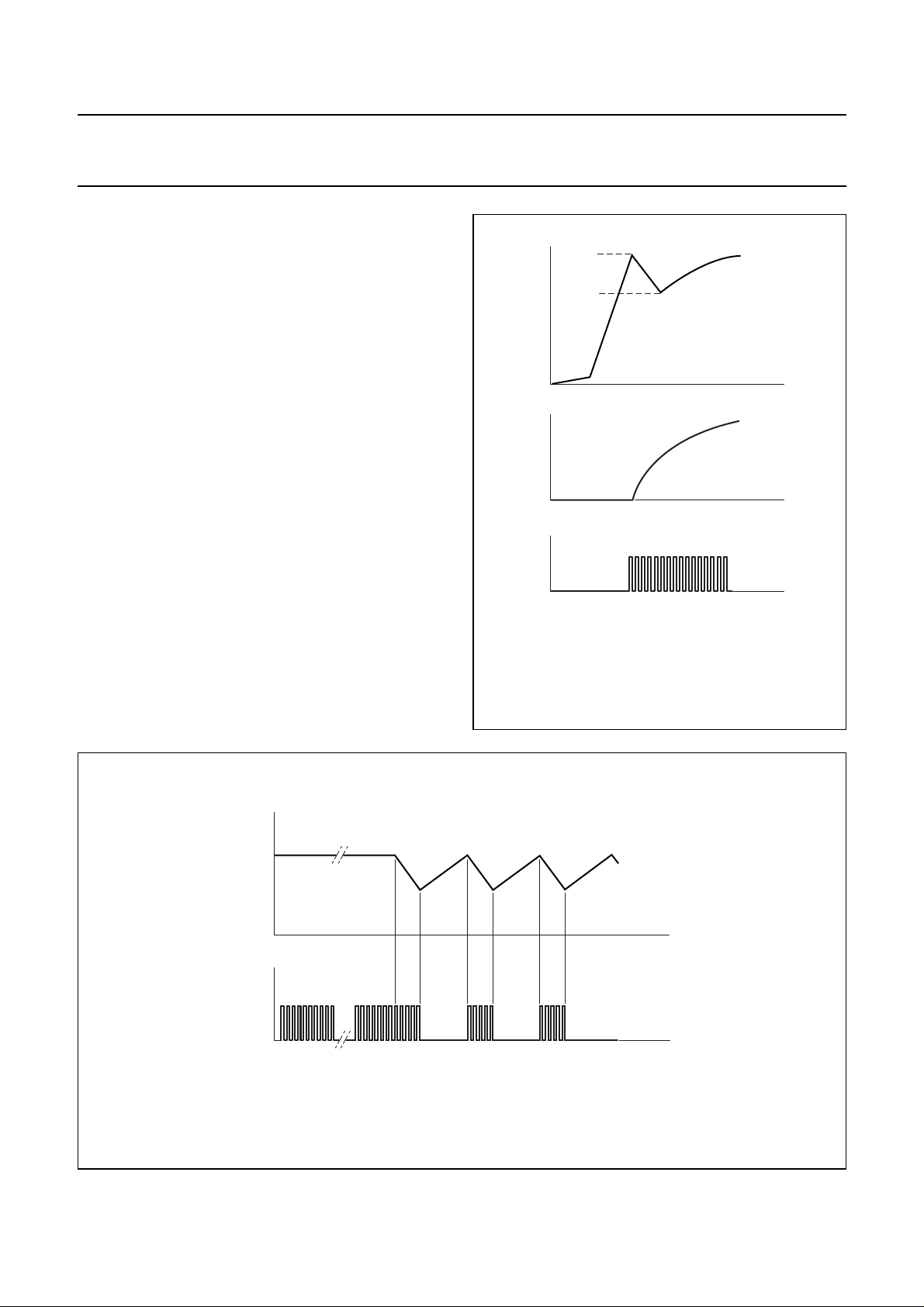
Start-up current source and Vaux management
A versatile on-chip start-up current source makes an
external, highly dissipating, trickle-charge circuit
unnecessary. See Fig.2 for the block diagram of the IC.
The start-up current source derives power from the mains
via pin Vin (drain). It supplies current (see symbols
‘Istart-low’ and ‘Istart-high’ of Chapter “Characteristics”) to
charge the Vaux (IC supply) capacitor and at the same
time provides current to the control circuitry of the IC. Once
the Vaux capacitor is charged to its start-up voltage level
(11 V), the on-chip oscillator starts oscillating and the IC
starts switching the power MOSFET. Power is then
supplied to the load capacitor via the secondary winding.
Figure 1 shows a typical flyback application diagram.
The Vaux capacitor is also supplied by an auxiliary
winding on the primary side. This winding is coupled to the
secondary side winding supplying the output capacitor.
As the output capacitor voltage increases and approaches
its nominal value, the re-supply of the Vaux capacitor is
done by the auxiliary winding. Figure 4 shows relevant
waveforms at start-up. For successful take over of supply
of Vaux capacitor by the auxiliary winding, it is important
that the re-supply of Vaux capacitor starts before its
voltage drops to its Under Voltage Lockout (UVLO) level of
8.05 V of the system and stops delivering power to the
output.
1999 Apr 20 4
Page 5
Philips Semiconductors Preliminary specification
GreenChip; SMPS module TEA1566
In case of output short circuit, the Vaux capacitor is no
longer supplied by the auxiliary winding and its voltage
drops till it reaches the UVLO level. If the output is an open
circuit, the output voltage will rise till it reaches the Over
Voltage Protection (OVP) level. The IC will detect this state
and stop switching.
In absence of switching of the power device, the Vaux
capacitor will not be re-supplied and its voltage will drop till
it reaches UVLO level. Once the Vaux voltage drops to
UVLO level, the start-up current source is re-activated and
it charges the Vaux capacitor to its start level and the
system goes through a cycle similar to the start-up cycle.
Figure 5 shows the relevant waveforms during safe-restart
mode. The charging current (see symbol ‘Irestart-prot’ in
Chapter “Characteristics”) from the start-up circuit during
the safe-restart mode is lower than the normal start-up
current (see symbol ‘Istart-high’ in
Chapter “Characteristics”) in order to implement a low
“hiccup” duty cycle. This helps insure devices on the
output secondary winding do not get destroyed during
output short circuit, violating safety conditions.
The start-up current source also plays a key role in
implementation of burst mode stand-by (see symbol
‘Irestart-stby’ in Chapter “Characteristics”), which will be
explained later.
Vaux
Vout
Vgate
(1) Start-up current charges capacitor V
(2) Charging of capacitor V
11 V
(2)
8.05 V
(1)
switchingoff
.
is taken-over by the auxiliary winding.
aux
aux
Fig.4 Normal start-up waveforms.
t
t
t
MGR694
handbook, full pagewidth
(1) Start-up current source charges capacitor V
Vaux
Vgate
normal operation
.
aux
fault condition
(1)
switching off
Fig.5 Safe-start mode waveforms.
1999 Apr 20 5
MGR695
t
t
Page 6
Philips Semiconductors Preliminary specification
GreenChip; SMPS module TEA1566
Reference
All reference voltages are derived from a temperature
compensated, on-chip, band gap. The band gap reference
voltage is also used, together with an external resistor
connected at pin Iref, to generate accurate, temperature
independent, bias currents in the chip:
V
REF
I
REF
=
------------- R
REF
[A]
The frequency of the controller is also set by the reference
resistor Rref (also see Section “Oscillator”).
Sample and hold
GreenChip ICs employ voltage mode feedback for
regulating the output voltage. In primary feedback mode, a
novel sample and hold circuit is used. The sample and
hold circuit works by sampling the current into pin Dem,
which is related to the output voltage via Rdem, during the
time that the secondary current is flowing:
a × V
V
dem+
out=Iref
× R
dem+Vdem+
where:
is specified in chapter “Characteristics”
a = a constant determined by turn ratio of the
transformer.
This sampled current information is stored on the external
capacitor connected to pin Vctrl. The pulse width
modulator uses this voltage information to set the duty
cycle of operation for the power MOSFET. In secondary
feedback, the feedback voltage is provided by an
opto-coupler.
Oscillator
The oscillator is used to set the switching duty cycle by
comparing the oscillator ramp to the output of the error
amplifier in the pulse width modulator circuit.The oscillator
is fully integrated and works by charging and discharging
an internal capacitor between two voltage levels to create
a sawtooth waveform with a rising edge which is 80% of
the oscillator cycle. This ratio is used to set a maximum
switching duty cycle of 80% for the IC. The oscillator is
internally trimmed to 5% accuracy. The oscillator
frequency can be adjusted between 50 to 100 kHz
(see symbol f
osc-h-range
in Chapter “Characteristics”) by
changing the external reference resistor (see symbol Rref
in Chapter “Characteristics”) that sets the chip bias
currents. This gives additional flexibility to the power
supply designer in the choice of his system
components.The frequency is correlated with the value of
the reference resistor Rref (see Fig.6).
In Chapter “Characteristics” f
osc-typical
osc-l
and f
osc-h
and
, f
the Rref operating resistor range are specified.
MGR936
110
handbook, halfpage
high
frequency
(kHz)
90
55
low
frequency
(kHz)
45
Pulse width modulator
The pulse width modulator, which is made up of an
inverting error amplifier and a comparator (see Fig.2),
drives the power MOSFET with a duty cycle which is
inversely proportional to the voltage on pin Vctrl.
In primary feedback mode, this is the voltage on the
sample and hold capacitor and in secondary feedback
mode, this voltage is provided by an opto-coupler. A signal
from the oscillator sets a latch that turns on the power
MOSFET. The latch is reset by the signal from the pulse
width modulator or by the duty cycle limiting circuit.
The latching PWM mode of operation prevents multiple
switching of the power switch. The maximum duty cycle is
set internally at 80%.
Figure 7 shows the normal switching operation of the IC.
1999 Apr 20 6
70
50
30
10 20 30 40
(1) High frequency mode.
(2) Low frequency mode.
(1)
(2)
Fig.6 Frequency as function of the R
R
REF
(kΩ)
REF
35
25
15
value.
Page 7

Philips Semiconductors Preliminary specification
GreenChip; SMPS module TEA1566
Multi frequency control
The oscillator is also capable of working at a lower
frequency (see f
in Chapter “Characteristics”). A ratio
osc-l
of 1 : 2.5 is maintained between high and low frequency of
the oscillator. Low frequency operation is invoked if the
power supply is working at or below one ninth of its peak
power. By working at a lower frequency, the switching
losses in the power supply are reduced. A novel scheme
is used to ensure that the transfer of high to low frequency
and vice versa has no effect on the regulation of the output
voltage.
Gate driver
The gate driver has a totem-pole output stage that has
current sourcing capability of 120 mA and a current sink
capability of 550 mA. This is to enable fast turn on and turn
off of the power device for efficient operation.
A lower driver source current has been chosen in order to
limit the ∆V/∆t at switch-on. This is advantageous for EMI
(ElectroMagnetic Interference) and reduces the current
spike across Rsense.
Demagnetization protection
This feature guarantees discontinuous conduction mode
operation for the power supply which simplifies the design
of feedback control and gives faster transient response.
Demagnetization protection is an additional protection
feature that protects against saturation of the
transformer/inductor. Demagnetization protection also
protects the power supply components against excessive
stresses at start-up, when all energy storage components
are completely discharged. The converter is cycle by cycle
protected during shorted output system fault condition due
to the demagnetization protection. The value of the
demagnetization resistor (R
) can be calculated with the
dem
formula given in Section “Sample and hold”.
Negative clamp
The negative clamp circuit does not let the voltage on
pin Dem go below −0.4 V, when the auxiliary winding
voltage goes negative during the time that the power
device is turned on, to ensure correct operation of the IC.
Over voltage protection
An Over Voltage Protection (OVP) mode has been
implemented in the GreenChip series. This circuit works
by sensing the Vaux voltage. If the output voltage exceeds
the preset voltage limit, the OVP circuit turns off the power
MOSFET. With no switching of the power device, the Vaux
capacitor is not re-supplied and discharges to UVLO level
and the system goes into the low dissipation safe-restart
mode described earlier. The system recovers from the
safe-restart mode only if the OVP condition is removed.
Over current protection
Cycle by cycle Over Current Protection (OCP) is provided
by sensing the voltage on an external resistor which is
connected to the source of the power MOSFET.
The voltage on the current sense resistor, which reflects
the amplitude of the primary current, is compared
internally with a reference voltage using a high speed
comparator. This threshold voltage is specified as V
th(Imax)
in the chapter “Characteristics”. The maximum primary
V
(protection) current is therefore: [A]
I
prot
th Imax()
=
-----------------------R
sense
If the power device current exceeds the current limit, the
comparator trips and turns off the power device.
The power device is typically turned off in 210 ns
(see tDin Chapter “Characteristics”).
The availability of the current sense resistor off-chip for
programming the OCP trip level increases design flexibility
for the power supply designer. An off-chip current sense
resistor also reduces the risk of an OCP condition being
sensed incorrectly. At power MOSFET turn-on the
∆V/∆t limiters capacitance discharge current does not
have to flow through the sense resistor, because this
capacitor can be connected between drain and source of
the power MOSFET directly.
The Leading Edge Blanking (LEB) circuit works together
with the OCP circuit and inhibits the operation of the OCP
comparator for a short duration (see t
LEB
in
Chapter “Characteristics”) when the power device is
turned on. This ensures that the power device is not turned
off prematurely due to false sensing of an OCP condition
because of current spikes caused by discharge of
primary-side snubber and parasitic capacitances.
LEB time is not fixed and it tracks the oscillator frequency.
1999 Apr 20 7
Page 8

Philips Semiconductors Preliminary specification
GreenChip; SMPS module TEA1566
Over temperature protection
Protection against excessive temperature is provided by
an analog temperature sensing circuit that turns off the
power device when the temperature exceeds typically
140 °C.
On/off mode
The expensive mains switch can be replaced by an
in-expensive functional switch by using the on/off mode.
Figure 13 shows a flyback converter configured to use the
on/off mode. Depending upon the position of switch S1,
either voltage close to ground or a voltage of greater than
typical 2.5 V exists on pin OOB.
The difference between these voltages is detected
internally by the IC. The IC goes into the off-mode if the
voltage is low, where it consumes a current of typical
350 µA (see Iin-off in Chapter “Characteristics”). If the
voltage on pin OOB is typically 2.5 V (see Von/off in
Chapter “Characteristics”), the IC goes through the
start-up sequence and commences normal operation.
In Fig.14 a Mains Under Voltage Lock Out (MUVLO)
function has been created using 3 resistors. Assuming that
R3 is chosen very high ohmic, the GreenChip™ starts
operating if:
V
MAINS
R1
------- R2
V
OOB
R1 R2»()×≈
Burst mode stand-by
Pin OOB is also used to implement the burst mode
stand-by. In burst mode stand-by, the power supply goes
into a special low dissipation state where it typically
consumes less than 2 W of power. Figure 14 shows a
flyback converter using the burst mode stand-by feature.
The system enters burst mode when the microcontroller
closes switches S2 and S3 on the secondary side.
Switch S2 shorts the output capacitor to the voltage level
of the microcontroller capacitor. The output secondary
winding now supplies the microcontroller capacitor. When
the voltage on the microcontroller capacitor exceeds the
zener voltage (V
) the opto-coupler is activated which
z
sends a signal to pin OOB. In response to this signal, the
IC stops switching and goes into a “hiccup” mode.
Figure 7 shows the burst-mode operation graphically.
The hiccup mode during burst mode operation differs from
the hiccup in safe-restart mode during system fault. For
safe restart mode, the power has to be reduced. For burst
mode, sufficient power to supply the microcontroller has to
be delivered. To prevent transformer rattle, the
transformer peak current is reduced by a factor of 3.
Burst mode stand-by operation continues till the
microcontroller opens switches S2 and S3. The system
then goes through the start-up sequence and commences
normal switching behaviour.
In this way it is assured that the power supply only starts
working above a Vmains of e.g. 80 V. The bleeder current
through R1 should be low (e.g. 30 µA at 300 V).
1999 Apr 20 8
Page 9

Philips Semiconductors Preliminary specification
GreenChip; SMPS module TEA1566
handbook, full pagewidth
Vin
Vin
Vdrain
Vout
Vaux
Vgate
Iaux
burst mode
VµP
0
(1)
start up
sequence
normal
operation
over voltage
protection
output short
circuit
burst mode stand-by
normal
operation
MGR696
(1) All negative currents are currents out the chip.
Fig.7 Typical waveforms.
1999 Apr 20 9
Page 10

Philips Semiconductors Preliminary specification
GreenChip; SMPS module TEA1566
LIMITING VALUES
In accordance with the Absolute Maximum Rating System (IEC 134); unless noted all voltages are measured with
respect to pin GND.
SYMBOL PARAMETER CONDITIONS MIN. MAX. UNIT
V
I(max)
I
D
V
OOB
I
OOB
I
demag
V
ctrl
V
lsense
I
ref
V
aux
T
j
T
stg
V
es
maximum DC input voltage − 600 V
during inductive turn-off;
− 720 V
note 1
supply current − 7A
mode detect input voltage −0.3 +14 V
mode detect input current −+2mA
demagnetization input current −±1mA
feedback input voltage −0.3 +5 V
current sense input voltage −0.3 +5 V
reference input current −−1mA
auxiliary supply voltage −0.3 +18 V
operating junction temperature −10 +140 °C
storage temperature −40 +150 °C
electrostatic handling voltage class 2
human body model; note 3 − 2500 V
machine model; note 4 − 250 V
Notes
1. Repetitive clamped inductive turn-off energy <15 mJ.
2. Single pulse avalanche energy at T
<25°C: 570 mJ.
j
3. Equivalent to discharging a 100 pF capacitor through a 1.5 kΩ resistor.
4. Equivalent to discharging a 200 pF capacitor through a 0.75 mH coil.
THERMAL CHARACTERISTICS
SYMBOL PARAMETER VALUE UNIT
IC controller
R
R
th(j-a)
th(j-c)
thermal resistance from junction to ambient 70 K/W
thermal resistance from junction to case 31 K/W
Power FET
R
R
th(j-a)
th(j-c)
thermal resistance from junction to ambient 37 K/W
thermal resistance from junction to case 0.85 K/W
QUALITY SPECIFICATION
In accordance with
“SNW-FQ-611 part E”
.
1999 Apr 20 10
Page 11

Philips Semiconductors Preliminary specification
GreenChip; SMPS module TEA1566
CHARACTERISTICS
= −10 to +110 °C; Vin= 300 V; V
T
j
currents out of the chip are negative; all voltages are measured with respect to ground.
SYMBOL PARAMETER CONDITIONS MIN. TYP. MAX. UNIT
Input voltage and current on pin 9
V
dlow
I
in
I
in(off)
minimum start drain voltage 100 −−V
input current normal operation 20 60 100 µA
off mode current V
Start-up current source and Vaux management on pin 2
V
start
V
uvlo
V
hys
I
start(low)
I
start(high)
l
aux
I
restart(prot)
I
restart(stdby)
V
clamp
start-up voltage 10.4 11 11.6 V
under voltage lockout 7.4 8.05 8.6 V
operation voltage hysteresis V
start-up current 0 V < V
start-up current 0.5 V < V
IC supply current in high frequency mode 7.0 7.7 8.5 mA
restart current in protection mode −600 −530 −460 µA
restart current in stand-by mode −2.5 −2.1 −1.7 mA
clamp voltage level l
Reference input on pin 3
V
ref
R
ref
reference voltage capacitor pin Iref = 50 nF 2.37 2.47 2.57 V
operating resistor range 16.9 24.9 33.2 kΩ
Oscillator
f
osc-l
f
osc-h
δ
max
f
ratio
f
osc-h-range
low frequency low power mode;
high frequency normal mode;
maximum duty cycle f = f
ratio f
osc-h/fosc-l
range of f
osc-h
Demagnetization input on pin 6
V
th(comp)
t
PD
demag comparator threshold V
propagation delay to output
buffer
I
bias
V
clamp(neg)
V
clamp(pos)
input bias current V
negative clamp level I
positive clamp level I
Sample and hold input on pin 6
I
dem
l
) sample threshold current % of Idem 78 83 88 %
th(sh
t
PD
normal control current lref = 100 µA 90 100 110 µA
propagation delay of current
comparator
= 8.6 to 13 V; R
aux
= 24.9 kΩ±0.1%; all currents into the chip are positive and all
Iref
< 1.95 V 150 350 550 µA
OOB
start-Vuvlo
< 0.5 V −270 −230 −190 µA
aux
aux<Vstart
= 5 mA (non switching) 15 − 18 V
aux
2.60 2.95 3.30 V
−5.0 −3.0 −1.0 mA
27.5 29 30.5 kHz
C
=50nF
IREF
66 70 74 kHz
C
=50nF
IREF
osc-h
78 80 82 %
2.30 2.45 2.60
with changing R
decreasing 50 65 80 mV
dem
IREF
50 70 100 kHz
300 500 700 ns
=65mV −0.50
dem
= −500 µA −0.45 −0.35 0 V
dem
= 100µA 2.3 2.6 2.9 V
dem
(1)
−−0.10
(1)
µA
δVdemag/δt positive 170 450 730 ns
δVdemag/δt negative 20 90 160 ns
1999 Apr 20 11
Page 12

Philips Semiconductors Preliminary specification
GreenChip; SMPS module TEA1566
SYMBOL PARAMETER CONDITIONS MIN. TYP. MAX. UNIT
Over voltage protection on pin 2
V
OVP
t
d(OVP)
Isense and low power on pin 1
t
LEB
V
th(Imax)
t
d
V
th(lopower)
Control
dδ/dV gain f
V
CTRL(min)
V
CTRL(max)
I
CTRL(leak)
absolute maximum OVP level fixed maximum level 14.0 14.7 15.5 V
OVP delay time 350 550 800 ns
leading edge blanking time R
= 0.7 × R
ref
R
ref=Rref(nom)
= 1.3 × R
R
ref
ref(nom)
ref(nom)
180 260 340 ns
240 340 440 ns
415 470 560 ns
maximum current limit voltage 0.46 0.49 0.53 V
delay to MOSFET off time to MOSFET off at
150 210 270 ns
dV/dt = 200 mV/µs;
Cgs = 500 pF
threshold voltage for switch over to low power 155 165 175 mV
−95 −85 −75 %/V
−60 −50 −40 %/V
2.00 2.15 2.30 V
minimum control voltage on
osc-h
f
osc-l
pin 4
maximum control voltage on
2.90 3.05 3.20 V
pin 4
leakage current in/out on
note 1 −1 − +1 µA
pin 4
Over temperature protection
T
trip
temperature limit 130 140 155 °C
On/off/burst mode selection input on pin 7
V
V
on/off
burst
on/off trip level 2.3 2.5 2.8 V
burst mode trip level active 6.5 − 7.5 V
inactive −−5.5 V
I
OOB
output current on pin OOB V
> 400 mV; note 1 −5 − -0.1 µA
OOB
Power MOSFET 7N60E; note 2
V
DS(break)
R
DS(on)
drain-to-source breakdown
voltage
drain-to-source on-state
resistance
Tj=25°C;
Vgs = 0 V; Id = 0.25 mA
Tj=25°C;
Vgs=10V;Vaux=10V;
600 −−V
− 1.0 1.2 Ω
Id = 7A
Notes
1. Min. and max. values are guaranteed by design.
2. The power MOSFET outputs of these devices are similar to the Philips Semiconductor type PHP7N60. These
devices feature an excellent combination of fast switching, ruggedized device design, low on-resistance and cost
effectiveness.
1999 Apr 20 12
Page 13

Philips Semiconductors Preliminary specification
GreenChip; SMPS module TEA1566
160
handbook, halfpage
P
(W)
120
80
40
0
0 40 80 160
MGR937
120
T
case
Fig.8 Normalised power derating.
(°C)
3
10
handbook, halfpage
C
j
(pF)
2
10
10
11010
Coss
2103
VDS (V)
Fig.9 Junction capacitance.
MGR939
handbook, halfpage
3
a
2
1
0
−80
a = R
DS(on)/RDS(on)
ID= 6.2A; V
aux
at 25 °C.
>10V.
0 16080
Tj (°C)
Fig.10 Normalised drain-to-source on-state
resistance.
MGR938
1.2
handbook, halfpage
a
1.1
1
0.9
−100 0 100 200
Tj (°C)
Fig.11 Normalised drain-to-source breakdown
voltage.
MGR940
1999 Apr 20 13
Page 14

Philips Semiconductors Preliminary specification
GreenChip; SMPS module TEA1566
handbook, full pagewidth
I
VS= 50V; I
V
= 0.5 V; V
dem
IVC= 6mA; V
L =25 mH
MAX
=7A
aux
CLAMP
closed
=11V
= 720V
open
vc
Vctrl
Vaux
Vin
TEA1566
Dem Gnd
Fig.12 Clamped inductive test circuit.
APPLICATION INFORMATION
A converter using the GreenChip is usually a flyback or
a Buck converter that is made up of the EMI filter, full
bridge rectifier, filter capacitor, transformer, output
stage(s), and some snubber circuitry.
Depending upon the type of feedback used, either an
auxiliary winding (primary regulation) or an opto-coupler
(secondary regulation) is used. GreenChip, due to its
high level of integration uses very few external
components. A sense resistor converts the primary current
into a voltage on pin Isense. The IC uses this information
for setting the peak current in the converter.
A capacitor supplied by an auxiliary winding buffers the
internal supply of the IC and is connected on pin Vaux.
L
V
MGR941
S
Isense
I
MAX
CURRENT
SENSING
CIRCUIT
CLAMP
CIRCUIT
The primary side auxiliary winding is connected via a
resistor to pin Dem. Besides being used for
demagnetization protection, pin Dem is also used for
primary side regulation.
Pin OBB is a multi use pin and depending upon connection
can be used for implementation of the on/off/burst mode
functions.
Pin 8 is not connected and serves as a high voltage spacer
pin.
Pin Vin is the connection for the drain of the internal power
MOSFET and is a high voltage pin. The internal start-up
current source also uses this pin as a supply for charging
up the Vaux capacitor during start-up and safe-restart
modes.
The auxiliary winding is also used for primary mode output
voltage regulation. A resistor connected on pin Iref sets
the reference currents in the IC. A small capacitor
(0.2 to 2 nF) connected on pin Vctrl is used by the internal
sample and hold circuit for regulation in primary feedback
scheme. The same pin is also used for secondary sensing
and serves as the input for the signal from the
opto-coupler.
Pin Gnd is the ground connection pin.
1999 Apr 20 14
GreenChip is a versatile IC that can be used in flyback
and Buck converter topologies and can be configured to
work in different modes. The application diagrams on the
next pages give some examples.
For additional information also see:
•
Application note AN98011: “200 W SMPS with
TEA1504”
•
Application note AN98058: “75 W SMPS with
TEA1566”
.
Page 15

Philips Semiconductors Preliminary specification
GreenChip; SMPS module TEA1566
handbook, full pagewidth
mains
TEA1566
9
8
7
6
5
4
3
2
1
Vin
NC
OOB
Dem
Gnd
Vctrl
Iref
Vaux
Isense
R
SENSE
C
R
DEM
R
REF
REF
C
R
AUX
OOB
S1
MGR697
R
CTRL
output
Fig.13 Typical flyback configuration with secondary sensing and on/off feature.
1999 Apr 20 15
Page 16

Philips Semiconductors Preliminary specification
GreenChip; SMPS module TEA1566
handbook, full pagewidth
mains
TEA1566
9
8
7
6
5
4
3
2
1
Vin
NC
OOB
Dem
Gnd
Vctrl
Iref
Vaux
Isense
R1
R2
S1
S2
output
from
microcontroller
microcontroller
supply
V
z
R3
Fig.14 Flyback configuration using the burst mode stand-by, MUVLO and on/off features.
1999 Apr 20 16
MGR698
Page 17

Philips Semiconductors Preliminary specification
GreenChip; SMPS module TEA1566
handbook, full pagewidth
mains
output
Vin
9
NC
8
OOB
7
Dem
6
Gnd
TEA1566
5
4
3
2
1
Vctrl
Iref
Vaux
Isense
MGR699
Fig.15 Typical Buck configuration with primary sensing.
handbook, full pagewidth
mains
output
Vin
9
NC
8
OOB
7
Dem
6
Gnd
TEA1566
5
Vctrl
4
Iref
3
Vaux
2
Isense
1
MGR700
Fig.16 Typical Buck configuration with secondary sensing.
1999 Apr 20 17
Page 18

Philips Semiconductors Preliminary specification
GreenChip; SMPS module TEA1566
PACKAGE OUTLINES
SIL9P: plastic single in-line power package; 9 leads
D
d
seating plane
b
SOT131-2
non-concave
x
E
h
view B: mounting base side
A
B
j
A
1
D
h
2
E
19
Z
DIMENSIONS (mm are the original dimensions)
A
UNIT A
mm
Note
1. Plastic or metal protrusions of 0.25 mm maximum per side are not included.
1
max.
2.0
OUTLINE
VERSION
SOT131-2
4.6
4.2
e
b
b
cD
max.
1.1
p2
0.75
0.48
0.60
0.38
IEC JEDEC EIAJ
b
p
(1)
24.0
23.6
REFERENCES
w M
0 5 10 mm
scale
deD
h
20.0
10 2.54
19.6
1999 Apr 20 18
E
12.2
11.8
L
c
Q
(1)
E
h
6
3.4
3.1
Lj
Q
17.2
2.1
16.5
1.8
EUROPEAN
PROJECTION
0.25w0.03
ISSUE DATE
92-11-17
95-03-11
(1)
Z
x
2.00
1.45
Page 19

Philips Semiconductors Preliminary specification
GreenChip; SMPS module TEA1566
DBS9P: plastic DIL-bent-SIL power package; 9 leads (lead length 12 mm)
non-concave
D
d
j
x
E
h
B
D
h
view B: mounting base side
A
2
E
A
SOT157-2
19
e
Z
DIMENSIONS (mm are the original dimensions)
UNIT A A e
17.0
15.5
4.6
4.2
mm
Note
1. Plastic or metal protrusions of 0.25 mm maximum per side are not included.
OUTLINE
VERSION
SOT157-2
1
e
(1)
cD
0.75
0.48
0.60
0.38
IEC JEDEC EIAJ
deD
24.0
20.0
23.6
19.6
w M
b
p
E
h
12.2
10 5.08
11.8
REFERENCES
0 5 10 mm
scale
(1)
12bp
2.54
e
5.08
L
3
L
E
2
h
6
Q
LL3m
3.4
12.4
3.1
11.0
c
m
e
2.4
1.6
PROJECTION
2
4.3
EUROPEAN
2.1
1.8
v M
(1)
v
Qj
0.8
0.25w0.03
ISSUE DATE
95-03-11
97-12-16
Z
x
2.00
1.45
1999 Apr 20 19
Page 20

Philips Semiconductors Preliminary specification
GreenChip; SMPS module TEA1566
SOLDERING
Introduction to soldering through-hole mount
packages
This text gives a brief insight to wave, dip and manual
soldering. A more in-depth account of soldering ICs can be
found in our
Packages”
Wave soldering is the preferred method for mounting of
through-hole mount IC packages on a printed-circuit
board.
Soldering by dipping or by solder wave
The maximum permissible temperature of the solder is
260 °C; solder at this temperature must not be in contact
with the joints for more than 5 seconds.
Suitability of through-hole mount IC packages for dipping and wave soldering methods
DBS, DIP, HDIP, SDIP, SIL suitable suitable
“Data Handbook IC26; Integrated Circuit
(document order number 9398 652 90011).
PACKAGE
The total contact time of successive solder waves must not
exceed 5 seconds.
The device may be mounted up to the seating plane, but
the temperature of the plastic body must not exceed the
specified maximum storage temperature (T
printed-circuit board has been pre-heated, forced cooling
may be necessary immediately after soldering to keep the
temperature within the permissible limit.
Manual soldering
Apply the soldering iron (24 V or less) to the lead(s) of the
package, either below the seating plane or not more than
2 mm above it. If the temperature of the soldering iron bit
is less than 300 °C it may remain in contact for up to
10 seconds. If the bit temperature is between
300 and 400 °C, contact may be up to 5 seconds.
SOLDERING METHOD
DIPPING WAVE
(1)
stg(max)
). If the
Note
1. For SDIP packages, the longitudinal axis must be parallel to the transport direction of the printed-circuit board.
DEFINITIONS
Data sheet status
Objective specification This data sheet contains target or goal specifications for product development.
Preliminary specification This data sheet contains preliminary data; supplementary data may be published later.
Product specification This data sheet contains final product specifications.
Limiting values
Limiting values given are in accordance with the Absolute Maximum Rating System (IEC 134). Stress above one or
more of the limiting values may cause permanent damage to the device. These are stress ratings only and operation
of the device at these or at any other conditions above those given in the Characteristics sections of the specification
is not implied. Exposure to limiting values for extended periods may affect device reliability.
Application information
Where application information is given, it is advisory and does not form part of the specification.
LIFE SUPPORT APPLICATIONS
These products are not designed for use in life support appliances, devices, or systems where malfunction of these
products can reasonably be expected to result in personal injury. Philips customers using or selling these products for
use in such applications do so at their own risk and agree to fully indemnify Philips for any damages resulting from such
improper use or sale.
1999 Apr 20 20
Page 21

Philips Semiconductors Preliminary specification
GreenChip; SMPS module TEA1566
NOTES
1999 Apr 20 21
Page 22

Philips Semiconductors Preliminary specification
GreenChip; SMPS module TEA1566
NOTES
1999 Apr 20 22
Page 23

Philips Semiconductors Preliminary specification
GreenChip; SMPS module TEA1566
NOTES
1999 Apr 20 23
Page 24

Philips Semiconductors – a worldwide company
Argentina: see South America
Australia: 34 Waterloo Road, NORTH RYDE, NSW 2113,
Tel. +61 2 9805 4455, Fax. +61 2 9805 4466
Austria: Computerstr. 6, A-1101 WIEN, P.O. Box 213,
Tel. +43 1 60 101 1248, Fax. +43 1 60 101 1210
Belarus: Hotel Minsk Business Center, Bld. 3, r. 1211, Volodarski Str. 6,
220050 MINSK, Tel. +375 172 20 0733, Fax. +375 172 20 0773
Belgium: see The Netherlands
Brazil: see South America
Bulgaria: Philips Bulgaria Ltd., Energoproject, 15th floor,
51 James Bourchier Blvd., 1407 SOFIA,
Tel. +359 2 68 9211, Fax. +359 2 68 9102
Canada: PHILIPS SEMICONDUCTORS/COMPONENTS,
Tel. +1 800 234 7381, Fax. +1 800 943 0087
China/Hong Kong: 501 Hong Kong Industrial Technology Centre,
72 Tat Chee Avenue, Kowloon Tong, HONG KONG,
Tel. +852 2319 7888, Fax. +852 2319 7700
Colombia: see South America
Czech Republic: see Austria
Denmark: Sydhavnsgade 23, 1780 COPENHAGEN V,
Tel. +45 33 29 3333, Fax. +45 33 29 3905
Finland: Sinikalliontie 3, FIN-02630 ESPOO,
Tel. +358 9 615 800, Fax. +358 9 6158 0920
France: 51 Rue Carnot, BP317, 92156 SURESNES Cedex,
Tel. +33 1 4099 6161, Fax. +33 1 4099 6427
Germany: Hammerbrookstraße 69, D-20097 HAMBURG,
Tel. +49 40 2353 60, Fax. +49 40 2353 6300
Hungary: see Austria
India: Philips INDIA Ltd, Band Box Building, 2nd floor,
254-D, Dr. Annie Besant Road, Worli, MUMBAI 400 025,
Tel. +91 22 493 8541, Fax. +91 22 493 0966
Indonesia: PT Philips Development Corporation, Semiconductors Division,
Gedung Philips, Jl. Buncit Raya Kav.99-100, JAKARTA 12510,
Tel. +62 21 794 0040 ext. 2501, Fax. +62 21 794 0080
Ireland: Newstead, Clonskeagh, DUBLIN 14,
Tel. +353 1 7640 000, Fax. +353 1 7640 200
Israel: RAPAC Electronics, 7 Kehilat Saloniki St, PO Box 18053,
TEL AVIV 61180, Tel. +972 3 645 0444, Fax. +972 3 649 1007
Italy: PHILIPS SEMICONDUCTORS, Piazza IV Novembre 3,
20124 MILANO, Tel. +39 2 6752 2531, Fax. +39 2 6752 2557
Japan: Philips Bldg 13-37, Kohnan 2-chome, Minato-ku,
TOKYO 108-8507, Tel. +81 3 3740 5130, Fax. +81 3 3740 5077
Korea: Philips House, 260-199 Itaewon-dong, Yongsan-ku, SEOUL,
Tel. +82 2 709 1412, Fax. +82 2 709 1415
Malaysia: No. 76 Jalan Universiti, 46200 PETALING JAYA, SELANGOR,
Tel. +60 3 750 5214, Fax. +60 3 757 4880
Mexico: 5900 Gateway East, Suite 200, EL PASO, TEXAS 79905,
Tel. +9-5 800 234 7381, Fax +9-5 800 943 0087
Middle East: see Italy
Netherlands: Postbus 90050, 5600PB EINDHOVEN, Bldg. VB,
Tel. +31 40 27 82785, Fax. +31 40 27 88399
New Zealand: 2 Wagener Place, C.P.O. Box 1041, AUCKLAND,
Tel. +64 9 849 4160, Fax. +64 9 849 7811
Norway: Box 1, Manglerud 0612, OSLO,
Tel. +47 22 74 8000, Fax. +47 22 74 8341
Pakistan: see Singapore
Philippines: Philips Semiconductors Philippines Inc.,
106 Valero St. Salcedo Village, P.O. Box 2108 MCC, MAKATI,
Metro MANILA, Tel. +63 2 816 6380, Fax. +63 2 817 3474
Poland: Ul. Lukiska 10, PL 04-123 WARSZAWA,
Tel. +48 22 612 2831, Fax. +48 22 612 2327
Portugal: see Spain
Romania: see Italy
Russia: Philips Russia, Ul. Usatcheva 35A, 119048 MOSCOW,
Tel. +7 095 755 6918, Fax. +7 095 755 6919
Singapore: Lorong 1, Toa Payoh, SINGAPORE 319762,
Tel. +65 350 2538, Fax. +65 251 6500
Slovakia: see Austria
Slovenia: see Italy
South Africa: S.A. PHILIPS Pty Ltd., 195-215 Main Road Martindale,
2092 JOHANNESBURG, P.O. Box 7430 Johannesburg 2000,
Tel. +27 11 470 5911, Fax. +27 11 470 5494
South America: Al. Vicente Pinzon, 173, 6th floor,
04547-130 SÃO PAULO, SP, Brazil,
Tel. +55 11 821 2333, Fax. +55 11 821 2382
Spain: Balmes 22, 08007 BARCELONA,
Tel. +34 93 301 6312, Fax. +34 93 301 4107
Sweden: Kottbygatan 7, Akalla, S-16485 STOCKHOLM,
Tel. +46 8 5985 2000, Fax. +46 8 5985 2745
Switzerland: Allmendstrasse 140, CH-8027 ZÜRICH,
Tel. +41 1 488 2741 Fax. +41 1 488 3263
Taiwan: Philips Semiconductors, 6F, No. 96, Chien Kuo N. Rd., Sec. 1,
TAIPEI, Taiwan Tel. +886 2 2134 2886, Fax. +886 2 2134 2874
Thailand: PHILIPS ELECTRONICS (THAILAND) Ltd.,
209/2 Sanpavuth-Bangna Road Prakanong, BANGKOK 10260,
Tel. +66 2 745 4090, Fax. +66 2 398 0793
Turkey: Talatpasa Cad. No. 5, 80640 GÜLTEPE/ISTANBUL,
Tel. +90 212 279 2770, Fax. +90 212 282 6707
Ukraine: PHILIPS UKRAINE, 4 Patrice Lumumba str., Building B, Floor 7,
252042 KIEV, Tel. +380 44 264 2776, Fax. +380 44 268 0461
United Kingdom: Philips Semiconductors Ltd., 276 Bath Road, Hayes,
MIDDLESEX UB3 5BX, Tel. +44 181 730 5000, Fax. +44 181 754 8421
United States: 811 East Arques Avenue, SUNNYVALE, CA 94088-3409,
Tel. +1 800 234 7381, Fax. +1 800 943 0087
Uruguay: see South America
Vietnam: see Singapore
Yugoslavia: PHILIPS, Trg N. Pasica 5/v, 11000 BEOGRAD,
Tel. +381 11 62 5344, Fax.+381 11 63 5777
For all other countries apply to: Philips Semiconductors,
International Marketing & Sales Communications, Building BE-p, P.O. Box 218,
5600 MD EINDHOVEN, The Netherlands, Fax. +31 40 27 24825
© Philips Electronics N.V. 1999 SCA63
All rights are reserved. Reproduction in whole or in part is prohibited without the prior written consent of the copyright owner.
The information presented in this document does not form part of any quotation or contract, is believed to be accurate and reliable and may be changed
without notice. No liability will be accepted by the publisher for any consequence of its use. Publication thereof does not convey nor imply any license
under patent- or other industrial or intellectual property rights.
Internet: http://www.semiconductors.philips.com
Printed in The Netherlands 295002/50/01/pp24 Date of release: 1999 Apr 20 Document order number: 9397 750 03312
 Loading...