

Page 1
TDA1302_1 2 Wed Sep 14 13:30:56 1994
Philips Semiconductors Preliminary specification
Data amplifier and laser supply circuit for
CD player and read only optical systems
FEATURES
• Six input buffer amplifiers with low-pass filtering and with
virtually no offset
• HF data amplifier with a high or low gain mode
• Two built-in equalizers for single or double-speed mode
ensuring high performance in both modes
• Fully automatic laser control including stabilization and
an ON/OFF switch, plus a separate supply (V
DDL
) for
power reduction
• Adjustable laser bandwidth and laser switch-on current
slope
• Protection circuit to prevent laser damage due to supply
voltage dip
• Optimized interconnectiion between pick-up detector
and digital servo processor (TDA1301T)
• Wide supply voltage range
• Wide temperature range
GENERAL DESCRIPTION
The TDA1302T is a data amplifier and laser supply circuit
for three-beam pick-up detectors applied in a wide range
of mechanisms for Compact Disc and read only optical
systems. The device contains 6 amplifiers which amplify
and filter the focus and radial diode signals and provides
an equalized RF signal suitable for single or double speed
mode; the mode can be switched by means of the speed
control pin. The device can accommodate astigmatic,
single foucault and double foucault detectors and can be
applied to all N-sub laser/monitor diode units even though
the circuit has been optimized for the Philips CDM12
mechanisms and the digital servo controller TDA1301T.
After a single initial adjustment the circuit will maintain
control over the laser diode current thus resulting in a
constant light output power which is independent of
ageing. The IC is mounted in a small-outline package to
enable it to be mounted close to the laser pick-up unit on
the sledge.
TDA1302T
• Low power consumption.
QUICK REFERENCE DATA
SYMBOL PARAMETER CONDITIONS MIN. TYP. MAX. UNIT
V
DD
supply voltage (pin 18) 3.4 − 5.5 V
Diode current amplifiers
G
dn
I
os(d)
B 3 dB bandwidth I
amplification − 1.55 − dB
diode output offset current − − 100 nA
= 1.67 µA 50 − − kHz
i(d)
RFE amplifier (built-in equalizer)
t
d(eq)
t
d(f)
equalization delay fi= 0.3 MHz − 320 − ns
flatness delay double-speed − 5 − ns
Laser supply
I
o(l)
output current V
= 3 V − − −100 mA
DDL
ORDERING INFORMATION
TYPE NUMBER
NAME DESCRIPTION VERSION
PACKAGE
TDA1302T SO24 plastic small outline package; 24 leads; body width 7.5 mm SOT137-1
September 1994 2
Page 2
Philips Semiconductors Preliminary specification
VV
V
V
V
Fig.1 Schematic diagram for CD player.
Data amplifier and laser supply circuit for
CD player and read only optical systems
SCHEMATIC DIAGRAM
TDA1302T
September 1994 3
TDA1302_1 3 Wed Sep 14 13:30:56 1994
Page 3
TDA1302_1 4 Wed Sep 14 13:30:56 1994
Fig.2 Block diagram.
Philips Semiconductors Preliminary specification
Data amplifier and laser supply circuit for
CD player and read only optical systems
BLOCK DIAGRAM
TDA1302T
September 1994 4
Page 4
TDA1302_1 5 Wed Sep 14 13:30:56 1994
Fig.3 Pin configuration.
Philips Semiconductors Preliminary specification
Data amplifier and laser supply circuit for
CD player and read only optical systems
PINNING
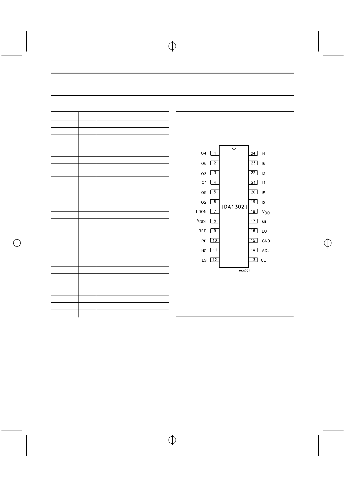
SYMBOL PIN DESCRIPTION
O4 1 output of diode current amplifier 4
O6 2 output of diode current amplifier 6
O3 3 output of diode current amplifier 3
O1 4 output of diode current amplifier 1
O5 5 output of diode current amplifier 5
O2 6 output of diode current amplifier 2
LDON 7 control pin for switching the laser
ON and OFF
V
DDL
RFE 9 equalized output voltage of sum
RF 10 unequalized output
HG 11 control pin for gain switch
LS 12 control pin for speed switch
CL 13 external capacitor
ADJ 14 reference input normally
GND 15 0 V supply; substrate connection
LO 16 current output to the laser diode
MI 17 laser monitor diode input
V
DD
I2 19 photo detector input 2 (central)
I5 20 photo detector input 5 (satellite)
I1 21 photo detector input 1 (central)
I3 22 photo detector input 3 (central)
I6 23 photo detector input 6 (satellite)
I4 24 photo detector input 4 (central)
8 laser supply voltage
signal of amplifiers 1 to 4
connected to ground via a resistor
(ground)
18 amplifier supply voltage
TDA1302T
September 1994 5
Page 5
TDA1302_1 6 Wed Sep 14 13:30:56 1994
Philips Semiconductors Preliminary specification
Data amplifier and laser supply circuit for
CD player and read only optical systems
FUNCTIONAL DESCRIPTION
The TDA1302T can be divided into two main sections, the
laser control circuit and the photo diode signal filter and
amplification section.
Laser control circuit
The main function of the laser control circuit is to control
the laser diode current in order to achieve a constant light
output power which is based on the current of the monitor
diode which is continuously monitored. The circuit is built
up into three parts.
The first part is the input stage which compares the
monitor diode current with a current which is 10 times the
value of the adjustable current. The adjustable current is
derived from a bandgap reference source, to be
temperature independent, and can be further adjusted by
the external resistor R
parameters of the laser/monitor diode unit to be used. The
difference is fed to the second part.
The second part is the integrator stage which makes use
of an external capacitor CL. This capacitor has two
different functions.
During switch-on of the laser current, it provides a current
slope of typically: dILO/dt ≅ 10−6/CL (A/s).
After switch-on it ensures that the bandwidth conforms to
the typical formula: fB≅ K × A
where A
represents the AC gain of an extra loop
ext
amplifier, if applied, and K = dI
determined by the laser/monitor unit.
is the average current (pin 17) at typical light
I
MON
emission power of the laser diode.
in order to adapt the circuit to the
ADJ
× 90−9/(CL × I
ext
monitor
/dI
laser
MON
which is
) (Hz).
TDA1302T
The third part is the power output stage, its input being the
integrator output signal. This stage has a separate supply
voltage (V
power consumption by supplying this pin with the minimum
voltage necessary.
It also has a laser diode protection circuit which is enabled
prior to the output drive transistor becoming saturated due
to a large voltage dip on V
lower current from the laser diode, which is normally
followed immediately by an increment of the voltage from
the external capacitor CL, which could cause damage to
the laser diode at the end of the voltage dip. The protection
circuit prevents an increment of the capacitor voltage and
thus offers full protection to the laser diode under these
circumstances.
Photo diode signal filter and amplification section
This section has 6 identical current amplifiers. Amplifiers 1
to 4 are designed to amplify the focus photo diode signals.
Each amplifier has two outputs, an LF output and an
internal RF output. Amplifiers 5 and 6 are used for the
radial photo diode currents and have only an LF output. All
6 output signals are low-pass filtered with a corner
frequency at 65 kHz. The internal RF output signals are
summed together and converted into a voltage by means
of a selectable transresistance of 120 kΩ or 240 kΩ. This
signal is available directly at pin 10, however, there is also
an unfiltered signal available at pin 9. The equalization
filter used has 2 different filter curves, one for single-speed
mode and one for double-speed mode.
) thereby offering the possibility of reduced
DDL
. Saturation will result in a
DDL
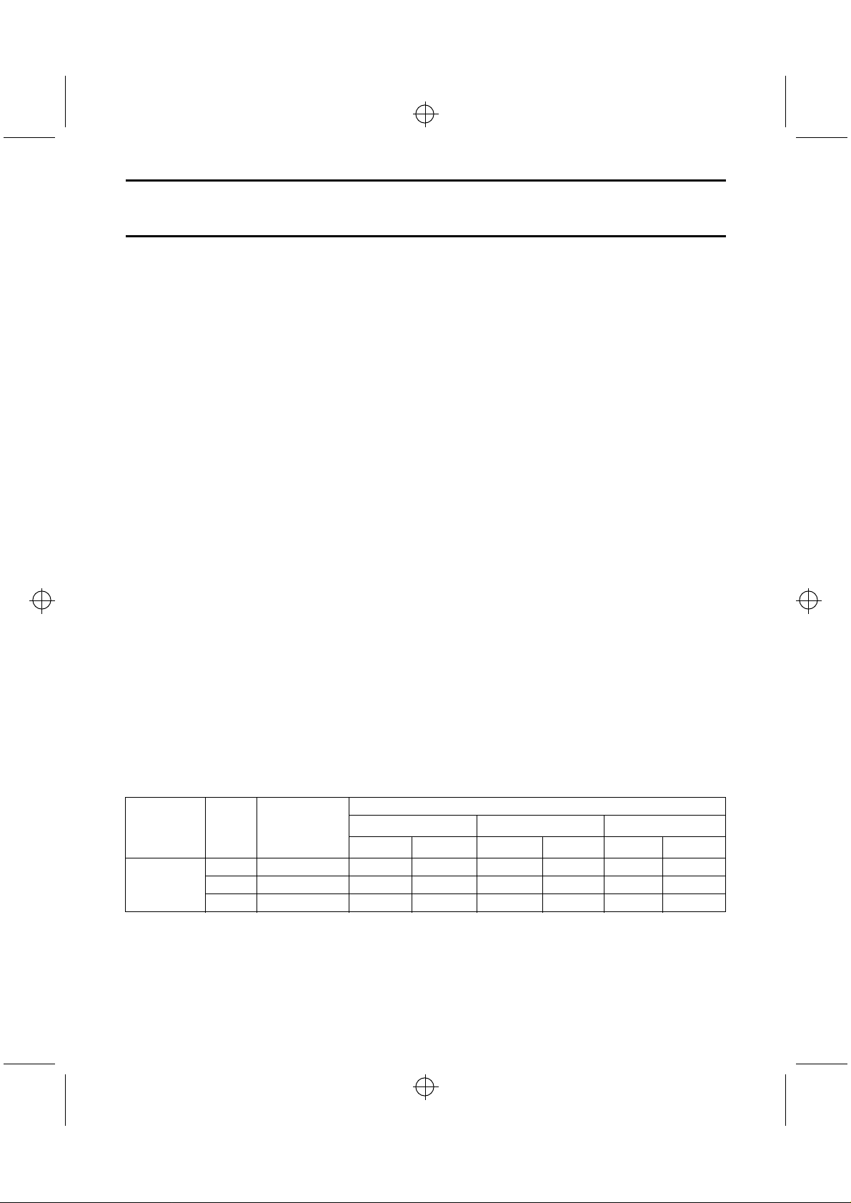
Table 1 Operational modes.
IF NOT
SWITCH PIN
CONNECTED
DEFAULT
GAIN SPEED LASER
HIGH LOW SINGLE DOUBLE ON OFF
HG 1 1 0 X X X X
Control pin
LS 1 X X 1 0 X X
LDON 1 X X X X 1 0
Note
1. Where X = don’t care.
September 1994 6
MODE
(1)
Page 6
TDA1302_1 7 Wed Sep 14 13:30:56 1994
Philips Semiconductors Preliminary specification
Data amplifier and laser supply circuit for
CD player and read only optical systems
TDA1302T
LIMITING VALUES
In accordance with the Absolute Maximum Rating System (IEC 134).
SYMBOL PARAMETER MIN. MAX. UNIT
V
DD
P
tot
T
stg
T
amb
supply voltage − 8.0 V
total power dissipation − 300 mW
storage temperature −65 +150 °C
operating ambient temperature −40 +85 °C
HANDLING
Classification A: human body model; C = 100 pF; R = 1500 Ω; V = ± 2000 V.
Charge device model: C = 200 pF; L = 2.5 µH; R = 0 Ω; V = 250 V.
THERMAL RESISTANCE
SYMBOL PARAMETER THERMAL RESISTANCE
R
th j-a
from junction to ambient in free air 60 K/W
QUALITY SPECIFICATION
In accordance with
“SNW-FQ-611 part E”
Reference Handbook”
. The handbook can be ordered using the code 9398 510 63011.
. The numbers of the quality specification can be found in the
“Quality
CHARACTERISTICS
VDD= 3.4 V; V
(R
= 750 Ω, C
ext
= 2.5 V; T
DDL
= 47 pF) at pin 9; unless otherwise specified.
ext
= 25 °C; R
amb
= 48 kΩ; HG = logic 1; LS = logic 1; with an external LP filter
ADJ
SYMBOL PARAMETER CONDITIONS MIN. TYP. MAX. UNIT
Supply
I
DD
V
DD
V
DDL
P
diss
amplifier supply current laser OFF − 8 − mA
amplifier supply voltage 3.4 − 5.5 V
laser control supply voltage 2.5 − 5.5 V
power dissipation laser OFF; VDD= 3.4 V − 27 − mW
Diode current amplifiers (1 to 6)
I
i(d)
N
eq
V
i(d)
V
o(d)
G
dn
I
os(d)
Z
o(d)
B 3 dB bandwidth I
G
mm
diode input current note 1 − − 10 µA
equivalent noise input − 1 − pA/√Hz
diode input voltage I
= 1.67 µA − 0.9 − V
i(d)
diode output voltage −0.2 − VDD− 1 V
amplification I
diode output offset current I
output impedance Idi= 1.67 µA; V
mismatch in amplification Idi= 1.67 µA;
= 1.67 µA;
i(d)
V
= 0 V; note 2
o(dn)
= I
csin
i(d)
= 0; note 3 − − 100 nA
tsin
o(dn)
= 1.67 µA 50 68 − kHz
1.43 1.55 1.67 dB
= 0 V 500 − − kΩ
− − 3 %
V
= V
o(dn)
o(dm)
September 1994 7
Page 7

TDA1302_1 8 Wed Sep 14 13:30:56 1994
Philips Semiconductors Preliminary specification
Data amplifier and laser supply circuit for
CD player and read only optical systems
TDA1302T
SYMBOL PARAMETER CONDITIONS MIN. TYP. MAX. UNIT
Data amplifier; equalized single and double speed
V
RFO
R
RF
DC output voltage I
= 0 − 0.3 − V
csin
transresistance fi= 100 kHz; note 4 100 120 143 kΩ
fi= 100 kHz; note 5 200 240 285 kΩ
V
SR
Z
t
d(eq)
t
d(f)
G
B
RFMO
RF
oRF
R
RF
output voltage note 6 − − VDD− 1.2 V
slew rate VSR= 1 V (p-p) − 6 − V/µs
output impedance fi= 1 MHz − 100 − Ω
equalization delay note 7 − 320 − ns
flatness delay (Φ/ω) LS = 1 or 0; notes 7 and 8 − 10.5 − ns
gain ratio note 8 4.5 6 − dB
unequalized output bandwidth I
= 1.67 µA 3 5 − MHz
i(d)
Control pins LDON, LS and HG (with 47 kΩ internal pull-up resistor)
V
IL
V
IH
I
IL
LOW level input voltage −0.2 − +0.5 V
HIGH level input voltage VDD− 1 − VDD+ 0.2 V
LOW level input current − − 100 µA
Laser output
V
o(l)
I
o(l)
output voltage I
= 100 mA −0.2 − VDD− 0.7 V
o(l)
output current − − −100 mA
Monitor diode input
V
) monitor input voltage I
i(mon
I
i(mon)
Reference source V
V
ref
monitor input current − − 2 mA
and laser adjustment current I
GAP
reference voltage R
∆T reference temperature drift R
SR
ref
I
ADJ
Z
i
d
/dt slew rate output current CL = 1 nF − 1 − mA/µs
lo(l)
M multiplying factor (I
reference supply rejection − − 1 %
adjustment current R
input impedance R
i(mon)/IADJ
) − 10 −
= −1 mA − VDD− 0.7 − V
i(mon)
ADJ
= 48 kΩ 1.15 1.24 1.31 V
ADJ
= 48 kΩ − 40 × 10−6−
ADJ
= 5.6 kΩ − − 200 µA
ADJ
= 48 kΩ − 1 − kΩ
ADJ
September 1994 8
Page 8

TDA1302_1 9 Wed Sep 14 13:30:56 1994
Philips Semiconductors Preliminary specification
Data amplifier and laser supply circuit for
CD player and read only optical systems
TDA1302T
Notes to the characteristics
1. The maximum input current is defined as the current in which the gain reaches its minimum. Increasing the supply
voltage to VDD= 5 V increases the maximum input current (see also Figs 4 and 5).
2. The gain increases if a larger supply voltage is used (see also Fig.6).
3. I
is the sum of the diode input currents 1 to 4; I
csin
is the sum of the diode input currents 5 and 6.
tsin
4. Transresistance 120 kΩ means LOW gain, selected if HG = logic 0 (see Table 1).
5. Transresistance 240 kΩ means HIGH gain, selected if HG = logic 1 (see Table 1).
6. Output voltage swing will be: V
SRRF
= V
RFMO
= V
RFO(p-p)
.
7. Refers to equalized output only.
8. For single speed the gain ratio is defined as gain difference between 1 MHz and 100 kHz, while the flatness delay
is defined up to 1 MHz (see also Fig.7). For double speed the gain ratio is defined as gain difference between 2 MHz
and 200 kHz, while the flatness delay is defined up to 2 MHz.
Transfer function
The equalized amplifier including C
ext
and R
has the following transfer functions, where ‘rfe’ refers to equalized output
ext
only and ‘rf’ refers to equalized and not equalized outputs.
FOR SINGLE SPEED (SP = LOGIC 1)
V
rfe
---------I
csin
1 ks2–
R
rf
-----------------------------------------------------------------------1 1 Q⁄ s ωos⁄ s2ω
2
ω
⁄
os
2
⁄+×+
os
1
----------------------1 s ω
⁄+
×××=
-----------------------------------------1 sR
1
extCext
1
×+
(1)
FOR DOUBLE SPEED (SP = LOGIC 0)
V
---------I
csin
rfe
R
rf
1 ks2–
------------------------------------------------------------------------1 1 Q⁄ s ωod⁄ s2ω
2
⁄
ω
os
××=
2
⁄+×+
od
1
-----------------------------------------1 sR
×+
extCext
The denominator forms the denominator of a Bessel low-pass filter.
Table 2 Transresistance.
SYMBOL DESCRIPTION TYP. UNIT
k internally defined 4
ω
os/ω1
= ωod/ω
2
internally defined 1.094
Q internally defined 0.691
ωod= 2 × ω
R
RF
R
ext
C
ext
os
internally defined 17.6 × 10
see Chapter “Characteristics” −
external resistor 750 Ω
external capacitor 47 pF
September 1994 9
(2)
−6
rad/s
Page 9

TDA1302_1 10 Wed Sep 14 13:30:56 1994
V
V
V
Fig.4 Maximum input current as a function of VDD.
↑ =test limit.
BBB
BBB
Fig.5 Output current as a function of input current.
→ =test limit.
Philips Semiconductors Preliminary specification
Data amplifier and laser supply circuit for
CD player and read only optical systems
TDA1302T
September 1994 10
Page 10

TDA1302_1 11 Wed Sep 14 13:30:56 1994
I
Fig.6 Gain as a function of VDD.
↓ = test limit.
Fig.7 Transfer for single speed.
The dashed line = delay (ns); the solid line = gain (dB).
Philips Semiconductors Preliminary specification
Data amplifier and laser supply circuit for
CD player and read only optical systems
TDA1302T
September 1994 11
Page 11

TDA1302_1 12 Wed Sep 14 13:30:56 1994
Fig.8 Equivalent internal pin diagrams.
Philips Semiconductors Preliminary specification
Data amplifier and laser supply circuit for
CD player and read only optical systems
INTERNAL PIN CONFIGURATION
TDA1302T
September 1994 12
Page 12

TDA1302_1 13 Wed Sep 14 13:30:56 1994
Fig.9 Application of the CDM12 laser/monitor diode unit.
Fig.10 Application of the CDM12 pick-up unit.
Philips Semiconductors Preliminary specification
Data amplifier and laser supply circuit for
CD player and read only optical systems
APPLICATION INFORMATION
The TDA 1302T is optimized for Philips CDM12
mechanisms and, subsequently, this application is
preferred.
Application with Philips CDM12
The CDM12 mechanism uses an N sub-laser diode
together with a P sub-monitor diode and, since TDA1302T
TDA1302T
is optimized for this type, besides the standard
components CL and R
are required as illustrated in Fig.9.
As two central spot diodes are summed together inside the
pick-up unit, one input pin remains unused as shown in
Fig.10. Unused central spot inputs should be connected to
ground in order to eliminate noise contribution to the RF
and RFE signals.
, no other external components
ADJ
September 1994 13
Page 13

TDA1302_1 14 Wed Sep 14 13:30:56 1994
Fig.11 Applications of the laser/monitor units.
Philips Semiconductors Preliminary specification
Data amplifier and laser supply circuit for
CD player and read only optical systems
Application of other mechanisms
The TDA1302T can accommodate all laser/monitor
configurations with an N sub-laser diode. When an N
sub-monitor diode is used, external circuitry is required as
illustrated in Figs 11(a) to 11(d). Most of these
laser/monitor diode units have a variable resistor (Rm) in
parallel with the monitor diode which has been
pre-adjusted so that the voltage drop across this resistor
has a specific value at nominal laser diode output power.
The four circuits given each detail specific values for some
frequently used pick-up units as given in Table 3. Each
circuit has its own advantages. All circuits illustrated make
use of the fixed voltage (<200 mV) across the built-in
monitor resistor.
TDA1302T
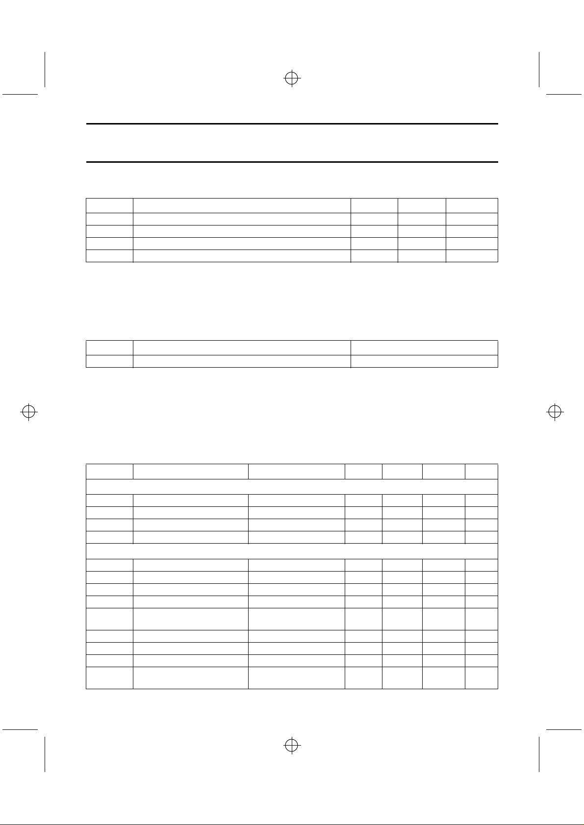
Table 3 Pick-up units.
PICK-UP
UNIT
SLD104U Sony corporation KSM210 (Sony)
LT022MS Sharp corporation KSM210 (Sony)
RLD-78MA Rohm corporation KSM210 (Sony)
SF91 Sony corporation CDV90V1 (Sanyo)
MANUFACTURER APPLICATION
HOP-M3TR
(Hitachi)
September 1994 14
Page 14

TDA1302_1 15 Wed Sep 14 13:30:56 1994
Philips Semiconductors Preliminary specification
Data amplifier and laser supply circuit for
CD player and read only optical systems
PROPERTIES OF CIRCUIT FIG.11(a)
It is important that the Vd(D1) approaches Vbe(T1) at
approximately 150 µA, that is why a small diode has been
applied such as the BA482. Additional adjustment may be
necessary. this depends on the matching of Vd(D1) and
Vbe(T1) and the permitted tolerance on the laser current.
The advised adjustment procedure is as follows:
1. Ensure that R
beginning of the adjustment.
2. Adjust R
as indicated in Table 4.
Table 4 Variable resistor (R
PICK-UP UNIT MANUFACTURER VRm (mV)
SLD104U Sony corporation 150
LT022MS Sharp corporation 150
RLD-78MA Rohm corporation 150
SF90 Sanyo corporation 180
SF91 Sanyo corporation 180
Table 5 Further circuit properties of Fig.11.
FIGURE PROPERTIES
ADJ
(a)
(b)
(c)
(d)
has the highest impedance at the
ADJ
until the voltage across Rm has the value
) voltage adjustment.
m
single supply voltage
only a few components are required;
2R, 1T and 1D
supply voltage independent
single supply voltage
only a few components are required;
1R, 2T and 1D
supply voltage independent
no extra adjustment necessary if T1 and T2
match
only a few components are required;
1R and 2T
supply voltage independent
no extra adjustment necessary
better power efficiency than (b)
single supply voltage
supply voltage independent
no extra adjustment necessary
no matching components required
TDA1302T
In Figs 11(b) to 11(d) solutions have been given requiring
no adjustment. R
R
= 12.4Re/VRm at P
ADJ
Examples of advised values applicable to Fig.11(b), (c)
and (d) are given in Table 6.
Table 6 Advised circuit values.
PICK-UP
UNIT
SLD104U Sony corporation 620 51
LT022MS Sharp corporation 620 51
RLD-78MA Rohm corporation 620 51
SF90 Sanyo corporation 750 51
(1)
SF91
Note
1. Notwithstanding that the SF91 specification details an
astigmatic detection system, TDA1301T requires a
single Foucault parameter setting.
Figures 12 and 13 give the application diagrams of the
pick-up unit of the mechanisms as previously indicated.
and Re can be calculated as follows:
ADJ
MANUFACTURER Re (Ω) R
Sanyo corporation 750 51
o(nom)
.
ADJ
(kΩ)
September 1994 15
Page 15

TDA1302_1 16 Wed Sep 14 13:30:56 1994
Fig.12 Application of pick-up units SLD104U, LT022MS and RLD-78MA.
Fig.13 Application of pick-up unit SF91.
Philips Semiconductors Preliminary specification
Data amplifier and laser supply circuit for
CD player and read only optical systems
TDA1302T
September 1994 16
Page 16

TDA1302_1 17 Wed Sep 14 13:30:56 1994
Philips Semiconductors Preliminary specification
Data amplifier and laser supply circuit for
CD player and read only optical systems
Circuit recommendations
PRINTED-CIRCUIT BOARD LAY-OUT ITEMS
It is advised to keep the output wires of the diode current
amplifiers separated from the input as much as possible to
prevent oscillations.
E
XTERNAL MONITOR DIODE CIRCUITRY
TDA1302T protects the laser diode against damage due to
supply voltage transients. When any external circuitry is
used in the ‘laser diode-monitor diode’ chain, the safety of
the laser diode completely relies on the quality of this
external circuitry. Therefore, it should be noted that:
1. If such a circuit requires a supply voltage, make sure
that this voltage is present at least at the same
moment as V
2. It is advised not to implement integrating actions in this
external circuitry as this may conflict with the internal
integrator, especially during possible supply voltage
drops.
MEASUREMENT OF THE LASER DIODE CURRENT
It is advised not to connect any current meter directly in
series with the laser diode. A safe method is the inclusion
of a 1 Ω resistor, connected in series with the laser diode,
and measuring the voltage across this resistor.
or earlier.
DDL
TDA1302T
September 1994 17
Page 17

TDA1302_1 18 Wed Sep 14 13:30:56 1994
Fig.14 Plastic small outline package; 24 leads; body width 7.5 mm (SO24L; SOT137AH).
Dimensions in mm.
handbook, full pagewidth
7.6
7.4
10.65
10.00
A
MBC235 - 1
0.3
0.1
2.45
2.25
1.1
0.5
0.32
0.23
1.1
1.0
0 to 8
o
2.65
2.35
detail A
S
15.6
15.2
0.1 S
1 12
1324
pin 1
index
0.9
0.4
(4x)
0.25 M
(24x)
0.49
0.36
1.27
Philips Semiconductors Preliminary specification
Data amplifier and laser supply circuit for
CD player and read only optical systems
PACKAGE OUTLINE
TDA1302T
September 1994 18
Page 18

TDA1302_1 19 Wed Sep 14 13:30:56 1994
Philips Semiconductors Preliminary specification
Data amplifier and laser supply circuit for
CD player and read only optical systems
SOLDERING
Plastic small-outline packages
B
Y WAVE
During placement and before soldering, the component
must be fixed with a droplet of adhesive. After curing the
adhesive, the component can be soldered. The adhesive
can be applied by screen printing, pin transfer or syringe
dispensing.
Maximum permissible solder temperature is 260 °C, and
maximum duration of package immersion in solder bath is
10 s, if allowed to cool to less than 150 °C within 6 s.
Typical dwell time is 4 s at 250 °C.
A modified wave soldering technique is recommended
using two solder waves (dual-wave), in which a turbulent
wave with high upward pressure is followed by a smooth
laminar wave. Using a mildly-activated flux eliminates the
need for removal of corrosive residues in most
applications.
BY SOLDER PASTE REFLOW
Reflow soldering requires the solder paste (a suspension
of fine solder particles, flux and binding agent) to be
TDA1302T
applied to the substrate by screen printing, stencilling or
pressure-syringe dispensing before device placement.
Several techniques exist for reflowing; for example,
thermal conduction by heated belt, infrared, and
vapour-phase reflow. Dwell times vary between 50 and
300 s according to method. Typical reflow temperatures
range from 215 to 250 °C.
Preheating is necessary to dry the paste and evaporate
the binding agent. Preheating duration: 45 min at 45 °C.
EPAIRING SOLDERED JOINTS (BY HAND-HELD SOLDERING
R
IRON OR PULSE
Fix the component by first soldering two, diagonally
opposite, end pins. Apply the heating tool to the flat part of
the pin only. Contact time must be limited to 10 s at up to
300 °C. When using proper tools, all other pins can be
soldered in one operation within 2 to 5 s at between 270
and 320 °C. (Pulse-heated soldering is not recommended
for SO packages.)
For pulse-heated solder tool (resistance) soldering of VSO
packages, solder is applied to the substrate by dipping or
by an extra thick tin/lead plating before package
placement.
-HEATED SOLDER TOOL)
DEFINITIONS
Data sheet status
Objective specification This data sheet contains target or goal specifications for product development.
Preliminary specification This data sheet contains preliminary data; supplementary data may be published later.
Product specification This data sheet contains final product specifications.
Limiting values
Limiting values given are in accordance with the Absolute Maximum Rating System (IEC 134). Stress above one or
more of the limiting values may cause permanent damage to the device. These are stress ratings only and operation
of the device at these or at any other conditions above those given in the Characteristics sections of the specification
is not implied. Exposure to limiting values for extended periods may affect device reliability.
Application information
Where application information is given, it is advisory and does not form part of the specification.
LIFE SUPPORT APPLICATIONS
These products are not designed for use in life support appliances, devices, or systems where malfunction of these
products can reasonably be expected to result in personal injury. Philips customers using or selling these products for
use in such applications do so at their own risk and agree to fully indemnify Philips for any damages resulting from such
improper use or sale.
September 1994 19
 Loading...