

Page 1

INTEGRATED CIRCUITS
DATA SH EET
TDA1072A
AM receiver circuit
Product specification
File under Integrated Circuits, IC01
May 1984
Page 2

Philips Semiconductors Product specification
AM receiver circuit TDA1072A
GENERAL DESCRIPTION
The TDA1072A integrated AM receiver circuit performs the active and part of the filtering functions of an AM radio
receiver. It is intended for use in mains-fed home receivers and car radios. The circuit can be used for oscillator
frequencies up to 50 MHz and can handle r.f. signals up to 500 mV. R.F. radiation and sensitivity to interference are
minimized by an almost symmetrical design. The voltage-controlled oscillator provides signals with extremely low
distortion and high spectral purity over the whole frequency range even when tuning with variable capacitance diodes.
If required, band switching diodes can easily be applied. Selectivity is obtained using a block filter before the i.f. amplifier.
Features
• Inputs protected against damage by static discharge
• Gain-controlled r.f. stage
• Double balanced mixer
• Separately buffered, voltage-controlled and temperature-compensated oscillator, designed for simple coils
• Gain-controlled i.f. stage with wide a.g.c. range
• Full-wave, balanced envelope detector
• Internal generation of a.g.c. voltage with possibility of second-order filtering
• Buffered field strength indicator driver with short-circuit protection
• A.F. preamplifier with possibilities for simple a.f. filtering
• Electronic standby switch.
QUICK REFERENCE DATA
Supply voltage range V
Supply current range I
R.F. input voltage for S + N/N = 6 dB at m = 30% V
R.F. input voltage for 3% total harmonic
distortion (THD) at m = 80% V
A.F. output voltage with V
= 1 MHz; m = 30% and fm= 400 Hz V
f
i
A.G.C. range: change of V
= 2 mV;
i
for 1 dB change of V
i
o(af)
Field strength indicator voltage at
= 500 mV; R
V
i
= 2,7 kΩ V
L(9)
PACKAGE OUTLINE
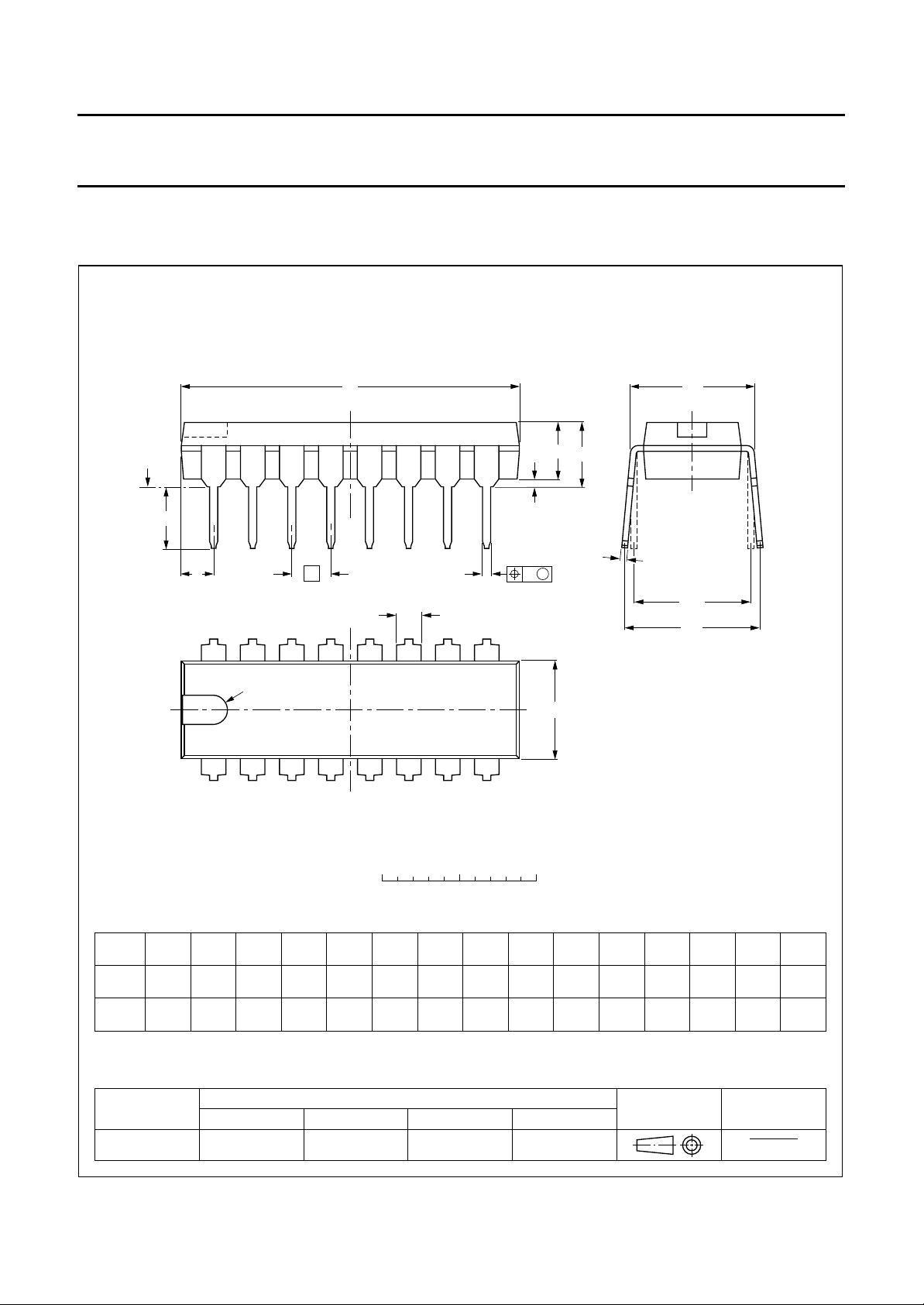
16-lead DIL; plastic (SOT38); SOT38-1; 1996 August 09.
P
P
i
i
o(af)
IND
7,5 to 18 V
15 to 30 mA
typ. 1,5 µV
typ. 500 mV
typ. 310 mV
typ. 86 dB
typ. 2,8 V
May 1984 2
Page 3
Philips Semiconductors Product specification
AM receiver circuit TDA1072A
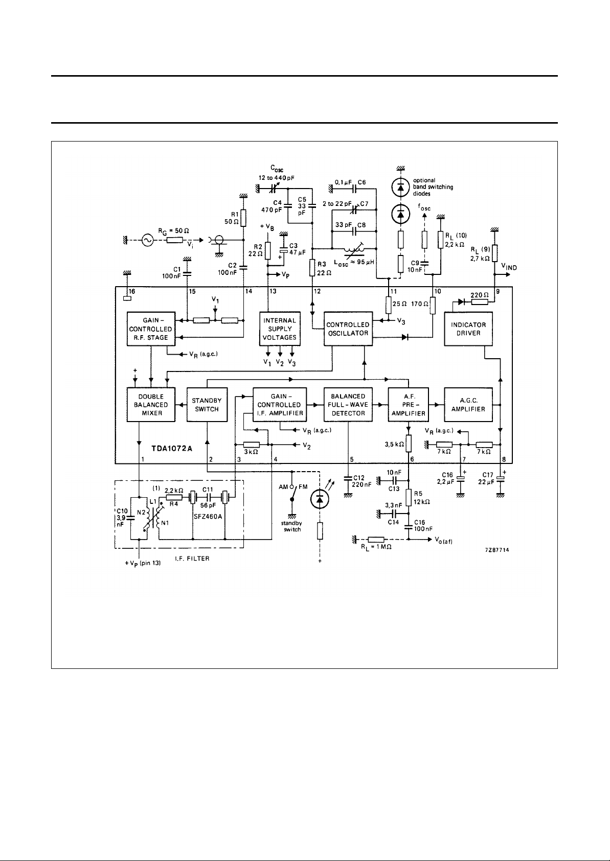
(1) Coil data: TOKO sample no. 7XNS-A7523DY; L1 : N1/N2 = 12/32; Qo = 65; QB = 57.
Filter data: Z
= 700 Ω at R
F
= 3 kΩ; ZI = 4,8 kΩ.
3-4
Fig.1 Block diagram and test circuit (connections shown in broken lines are not part of the test circuit).
May 1984 3
Page 4

Philips Semiconductors Product specification
AM receiver circuit TDA1072A
FUNCTIONAL DESCRIPTION
Gain-controlled r.f. stage and mixer
The differential amplifier in the r.f. stage employs an a.g.c. negative feedback network to provide a wide dynamic range.
Very good cross-modulation behaviour is achieved by a.g.c. delays at the various signal stages. Large signals are
handled with low distortion and the S/N ratio of small signals is improved. Low noise working is achieved in the differential
amplifier by using transistors with low base resistance.
A double balanced mixer provides the i.f. output signal to pin 1.
Oscillator
The differential amplifier oscillator is temperature compensated and is suitable for simple coil connection. The oscillator
is voltage-controlled and has little distortion or spurious radiation. It is specially suitable for electronic tuning using
variable capacitance diodes. Band switching diodes can easily be applied using the stabilized voltage V
buffered oscillator output (pin 10) is available for driving a synthesizer. If this is not needed, resistor R
L(10)
Gain-controlled i.f. amplifier
This amplifier comprises two cascaded, variable-gain differential amplifier stages coupled by a band-pass filter. Both
stages are gain-controlled by the a.g.c. negative feedback network.
. An extra
11-16
can be omitted.
Detector
The full-wave, balanced envelope detector has very low distortion over a wide dynamic range. Residual i.f. carrier is
blocked from the signal path by an internal low-pass filter.
A.F. preamplifier
This stage preamplifies the audio frequency output signal. The amplifier output has an emitter follower with a series
resistor which, together with an external capacitor, yields the required low-pass for a.f. filtering.
A.G.C. amplifier
The a.g.c. amplifier provides a control voltage which is proportional to the carrier amplitude. Second-order filtering of the
a.g.c. voltage achieves signals with very little distortion, even at low audio frequencies. This method of filtering also gives
fast a.g.c. settling time which is advantageous for electronic search tuning. The a.g.c. settling time can be further reduced
by using capacitors of smaller value in the external filter (C16 and C17). The a.g.c. voltage is fed to the r.f. and i.f. stages
via suitable a.g.c. delays. The capacitor at pin 7 can be omitted for low-cost applications.
Field strength indicator output
A buffered voltage source provides a high-level field strength output signal which has good linearity for logarithmic input
signals over the whole dynamic range. If the field strength information is not needed, R
can be omitted.
L(9)
Standby switch
This switch is primarily intended for AM/FM band switching. During standby mode the oscillator, mixer and a.f.
preamplifier are switched off.
Short-circuit protection
All pins have short-circuit protection to ground.
May 1984 4
Page 5

Philips Semiconductors Product specification
AM receiver circuit TDA1072A
RATINGS
Limiting values in accordance with the Absolute Maximum Rating System (IEC 134)
Supply voltage V
Total power dissipation P
Input voltage V
Input current I
Operating ambient temperature range T
Storage temperature range T
Junction temperature T
THERMAL RESISTANCE
= V
P
13-16
tot
max. 12 V
14-15
, −V
−V
14-16
V
14-16
, I15 max. 200 mA
14
amb
stg
j
, V
15-16
15-16
max. 20 V
max. 875 mW
max. 0,6 V
max. VPV
−40 to + 80 °C
−55 to + 150 °C
max. + 125 °C
From junction to ambient R
th j-a
= 80 K/W
DEVICE CHARACTERISTICS
= V
V
P
13-16
= 8,5 V; T
= 25 °C; fi = 1 MHz; fm = 400 Hz; m = 30%; fif = 460 kHz; measured in test circuit of Fig.1;
amb
unless otherwise specified
PARAMETER SYMBOL MIN. TYP. MAX. UNIT
Supplies
Supply voltage V
Supply current I
= V
P
13-16
= I
P
13
7,5 8,5 18 V
15 23 30 mA
R.F. stage and mixer
Input voltage (d.c. value) V
R.F. input impedance at V
R.F. input impedance at V
< 300 µVR
i
> 10 mV R
i
I.F. output impedance R
, V
14-16
, R
14-16
, C
C
14-16
, R
14-16
, C
C
14-16
1-16
C
1-16
15-16
15-16
15-16
15-16
15-16
− VP/2 − V
− 5,5 − kΩ
− 25 − pF
− 8 − kΩ
− 22 − pF
500 −−kΩ
− 6 − pF
Conversion transconductance
before start of a.g.c. I
1/Vi
− 6,5 − mA/V
Maximum i.f. output voltage, inductive
coupling to pin 1 V
1-13(p-p)
− 5 − V
D.C. value of output current (pin 1)
= 0 V I
at V
i
1
− 1,2 − mA
A.G.C. range of input stage − 30 − dB
R.F. signal handling capability:
input voltage for THD = 3% at m = 80% V
i(rms)
− 500 − mV
May 1984 5
Page 6

Philips Semiconductors Product specification
AM receiver circuit TDA1072A
PARAMETER SYMBOL MIN. TYP. MAX. UNIT
Oscillator
Frequency range f
osc
Oscillator amplitude (pins 11 to 12) V
External load impedance R
External load impedance for no oscillation R
Ripple rejection at V
= 100 Hz
f
P
(RR = 20 log [V
13-16/V11-16
Source voltage for switching diodes (6 × V
P(rms)
= 100 mV;
]) RR − 55 − dB
)V
BE
D.C. output current (for switching diodes) −I
Change of output voltage at
∆I11= 20 mA (switch to maximum load) ∆V
Buffered oscillator output
D.C. output voltage V
Output signal amplitude V
Output impedance R
Output current −I
I.F., a.g.c. and a.f. stages
D.C. input voltage V
I.F. input impedance R
C
I.F. input voltage for
THD = 3% at m = 80% V
Voltage gain before start of a.g.c. V
A.G.C. range of i.f. stages: change of
for 1 dB change of V
V
3-4
V
= 75 mV ∆V
3-4(ref)
A.F. output voltage at V
A.F. output voltage at V
3-4(if)
3-4(if)
;
o(af)
= 50 µVV
= 1 mV V
A.F. output impedance (pin 6) Z
Indicator driver
Output voltage at V
R
= 2,7 kΩ V
L(9)
Output voltage at V
R
= 2,7 kΩ V
L(9)
= 0 mV;
i
= 500 mV;
i
Load resistance R
11-12
12-11(ext)
12-11(ext)
11-16
11
11-16
10-16
10-16(p-p)
10
10(peak)
, V
3-16
4-16
3-4
3-4
3-4
3-4/V6-16
3-4
o(af)
o(af)
−3,5 − kΩ
o
9-16
9-16
L(9)
0,6 − 60 MHz
− 130 150 mV
0,5 − 200 kΩ
−−60 Ω
− 4,2 − V
0 − 20 mA
− 0,5 − V
− 0,7 − V
− 320 − mV
− 170 −Ω
−−3mA
− 2,0 − V
2,4 3 3,9 kΩ
− 7 − pF
− 90 − mV
− 68 − dB
− 55 − dB
− 130 − mV
− 310 − mV
− 20 150 mV
2,5 2,8 3,1 V
1,5 −−kΩ
May 1984 6
Page 7

Philips Semiconductors Product specification
AM receiver circuit TDA1072A
PARAMETER SYMBOL MIN. TYP. MAX. UNIT
Standby switch
Switching threshold at V
= −40 to + 80 °C
T
amb
on-voltage V
off-voltage V
on-current at V
off-current at V
2-16
2-16
OPERATING CHARACTERISTICS
= 8,5 V; fi= 1 MHz; m = 30%; fm= 400 Hz; T
V
P
R.F. sensitivity
R.F. input required for S + N/N = 6 dB V
R.F. input required for S + N/N = 26 dB V
R.F. input required for S + N/N = 46 dB V
R.F. input at start of a.g.c. V
R.F. large signal handling
R.F. input at THD = 3%; m = 80% V
R.F. input at THD = 3%; m = 30% V
R.F. input at THD = 10%; m = 30% V
A.G.C. range
o(af)
o(af)
; V
; V
i
i(ref)
i
i(ref)
for 1 dB change
= 500 mV ∆V
for 6 dB change
= 500 mV ∆V
Change of V
of V
Change of V
of V
Output signal
A.F. output voltage at
= 4 µV; m = 80% V
V
i
A.F. output voltage at V
THD at V
THD at V
= 1 mV; m = 80% d
i
= 500 mV; m = 30% d
i
Signal-to-noise ratio at V
Ripple rejection at V
= 100 mV; fP= 100 Hz
V
P(rms)
(RR = 20 log [V
P/Vo(af)
= 7,5 to 18 V;
P
0 − 2,0 V
3,5 − 20 V
−−200 µA
= 0 V −I
2-16
2-16
2
= 20 V I2−−10 µA
= 25 °C; measured in Fig.1; unless otherwise specified
amb
PARAMETER SYMBOL MIN. TYP. MAX. UNIT
i
i
i
i
i
i
i
i
i
o(af)
= 1 mV V
i
= 100 mV (S + N)/N − 58 − dB
i
= 2 mV;
i
o(af)
tot
tot
− 1,5 −µV
− 15 −µV
− 150 −µV
− 30 −µV
− 500 − mV
− 700 − mV
− 900 − mV
− 86 − dB
− 91 − dB
− 130 − mV
240 310 390 mV
− 0,5 − %
− 1 − %
]) RR − 38 − dB
May 1984 7
Page 8
Philips Semiconductors Product specification
AM receiver circuit TDA1072A
PARAMETER SYMBOL MIN. TYP. MAX. UNIT
Unwanted signals
Suppression of i.f. whistles at
= 15 µV; m = 0% related to
V
i
a.f. signal of m = 30%
≈ 2 × f
at f
at f
i
i
≈ 3 × f
if
if
I.F. suppression at r.f. input
for symmetrical input α
for asymmetrical input α
Residual oscillator signal at mixer output
at f
osc
at 2 × f
osc
α
2if
α
3if
if
if
I
1(osc)
I
1(2osc)
− 37 − dB
− 44 − dB
− 40 − dB
− 40 − dB
− 1 −µA
− 1,1 −µA
APPLICATION INFORMATION
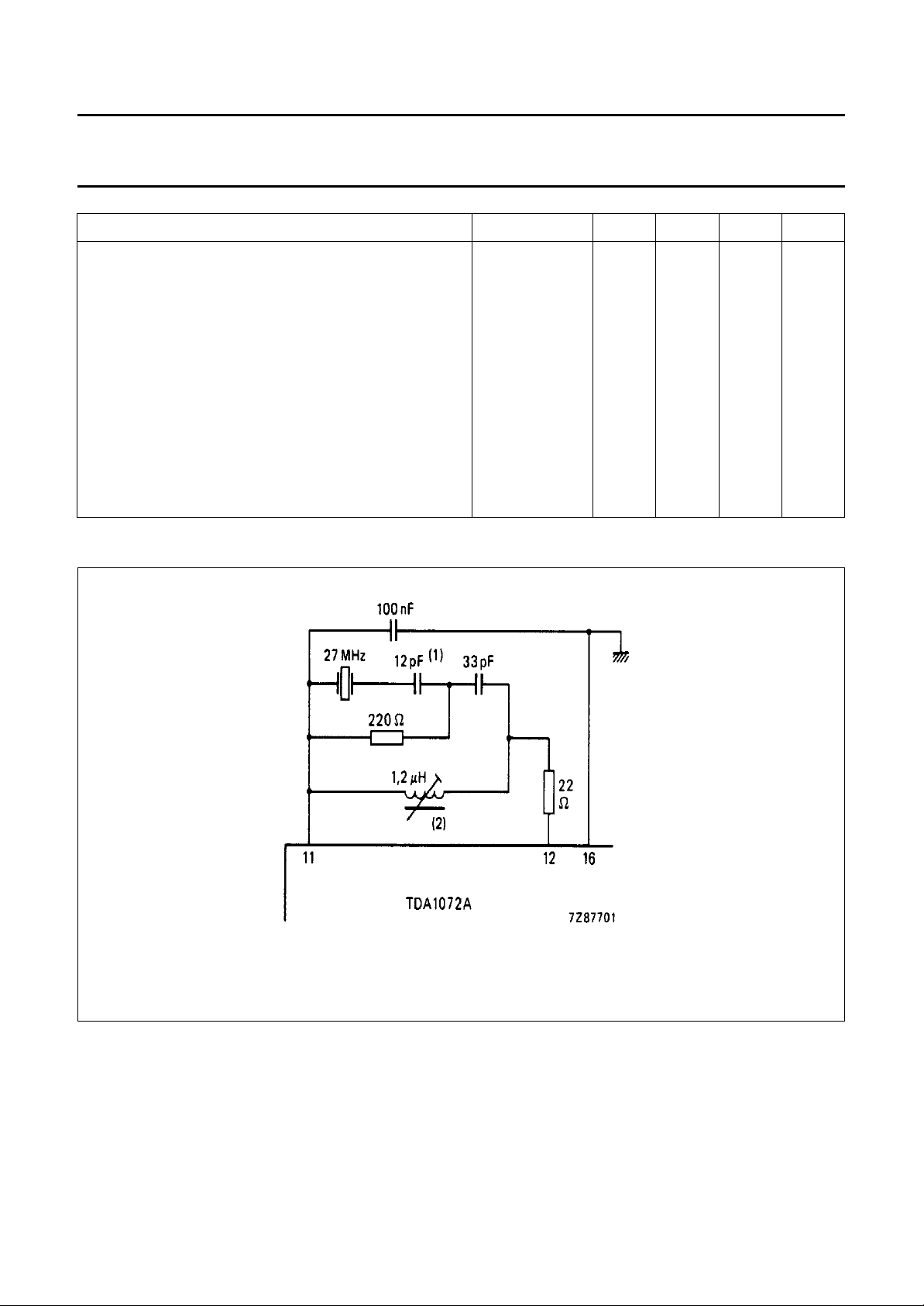
(1) Capacitor values depend on crystal type.
(2) Coil data: 9 windings of 0,1 mm dia laminated Cu wire on TOKO coil set 7K 199CN; Qo= 80.
Fig.2 Oscillator circuit using quartz crystal; centre frequency = 27 MHz.
May 1984 8
Page 9
Philips Semiconductors Product specification
AM receiver circuit TDA1072A
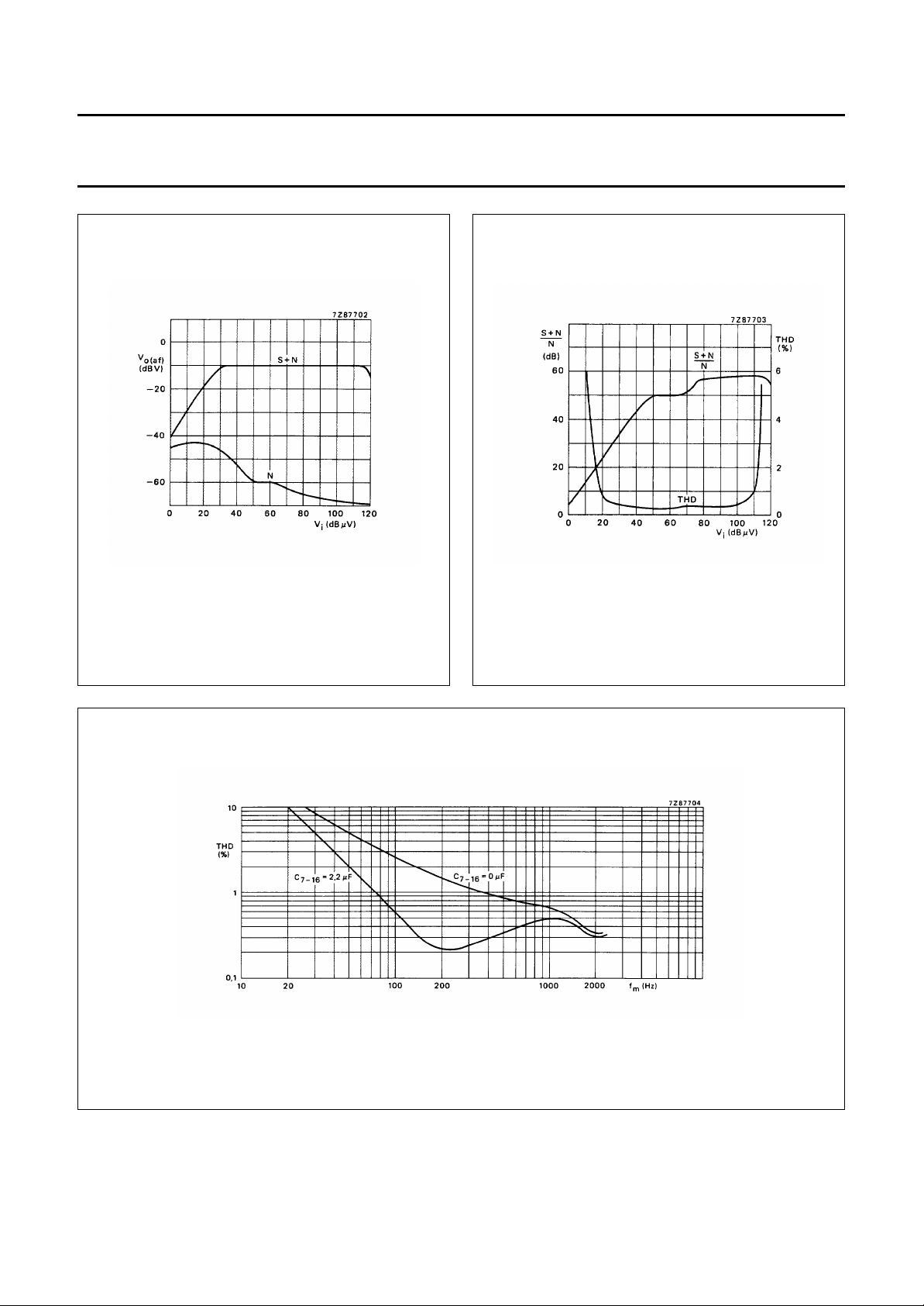
Fig.3 A.F. output as a function of r.f. input in the
circuit of Fig.1; fi = 1 MHz; fm= 400 Hz;
m = 30%.
Fig.4 Total harmonic distortion and (S + N)/N
as functions of r.f. input in the circuit of
Fig.1; m = 30% for (S + N)/N curve and
m = 80% for THD curve.
Fig.5 Total harmonic distortion as a function of modulation frequency at Vi = 5 mV; m = 80%;
measured in the circuit of Fig.1 with C
May 1984 9
7-16(ext)
= 0 µF and 2,2 µF.
Page 10
Philips Semiconductors Product specification
AM receiver circuit TDA1072A
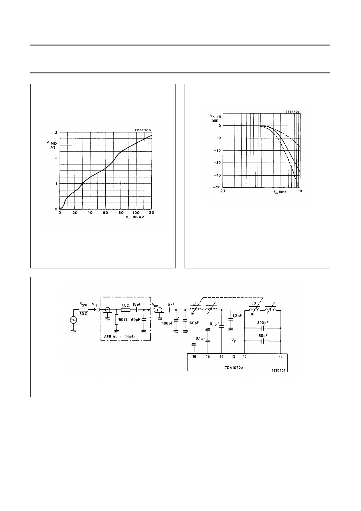
Fig.6 Indicator driver voltage as a function
of r.f. input in the circuit of Fig.1.
Fig.8 Car radio application with inductive tuning.
Fig.7 Typical frequency response curves from
Fig.1 showing the effect of filtering as
follows:
with i.f. filter;
− - − - − - with a.f. filter;
− − − − − with i.f. and a.f. filters.
May 1984 10
Page 11
Philips Semiconductors Product specification
AM receiver circuit TDA1072A
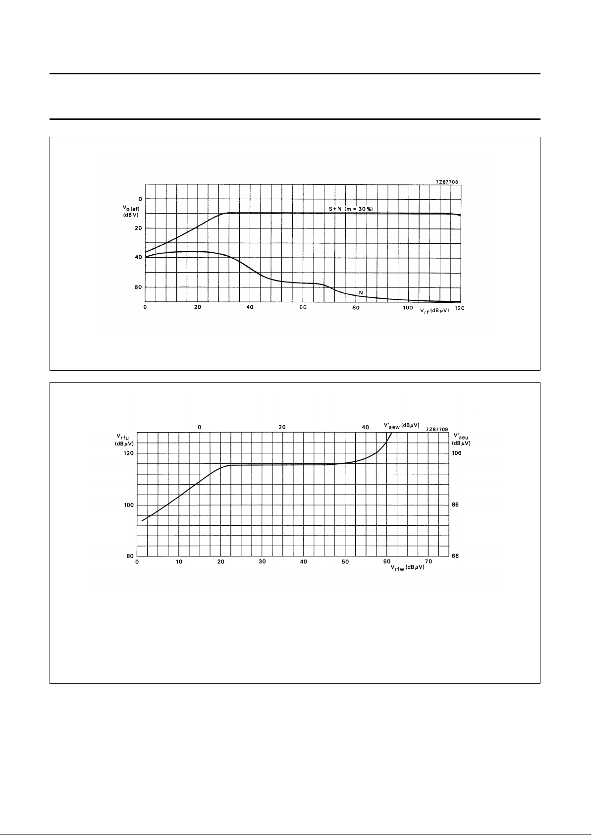
Fig.9 A.F. output as a function of r.f. input using the circuit of Fig.8 with that of Fig.1.
Fig.10 Suppression of cross-modulation as a function of input signal, measured in the circuit of Fig.8 with the input
circuit as shown in Fig.11. Curve is for Wanted V
aerial input, V'
Wanted signal (V'
Unwanted signal (V'
aew
, V'
are signals at the unloaded output of the aerial.
aeu
, V
aew
): fi = 1 MHz; fm = 400 Hz; m = 30%.
rfw
, V
aeu
): fi = 900 kHz; fm = 400 Hz; m = 30%.
rfu
/Unwanted V
o(af)
= 20 dB; V
o(af)
, V
are signals at the
rfw
rfu
Effective selectivity of input tuned circuit = 21 dB.
May 1984 11
Page 12
Philips Semiconductors Product specification
AM receiver circuit TDA1072A
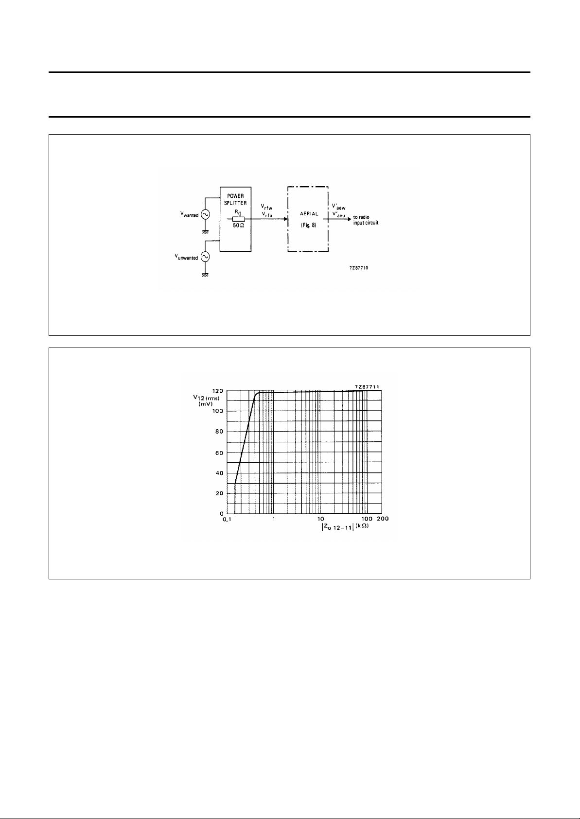
Fig.11 Input circuit to show cross-modulation suppression (see Fig.10).
Fig.12 Oscillator amplitude as a function of pin 11, 12 impedance in the circuit of Fig.8.
May 1984 12
Page 13
Philips Semiconductors Product specification
AM receiver circuit TDA1072A
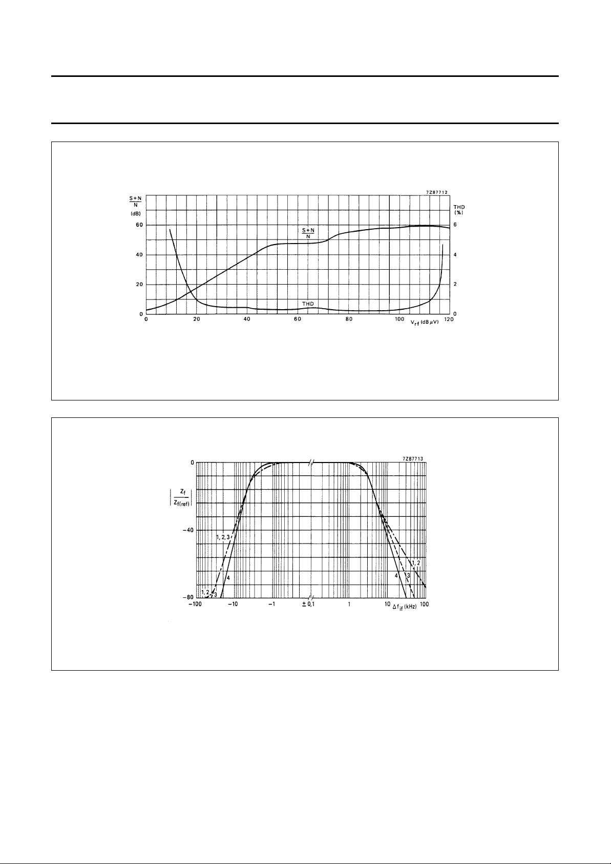
Fig.13 Total harmonic distortion and (S + N)/N as functions of r.f. input using the circuit of Fig.8 with that of Fig.1.
Fig.14 Forward transfer impedance as a function of intermediate frequency for filters 1 to 4 shown
in Fig.15; centre frequency = 455 kHz.
May 1984 13
Page 14
Philips Semiconductors Product specification
AM receiver circuit TDA1072A
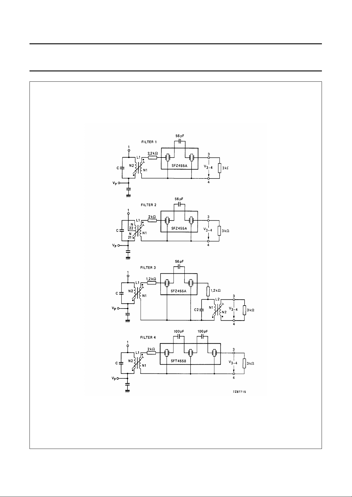
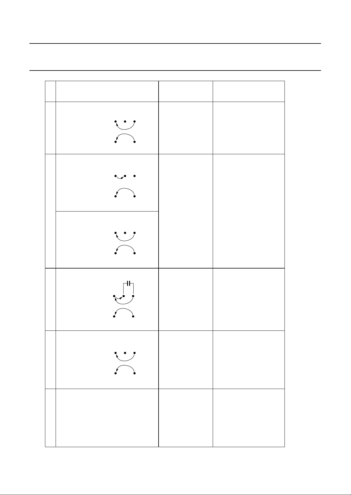
Fig.15 I.F. filter variants applied to the circuit of Fig.1. For filter data, refer to Table 1.
May 1984 14
Page 15
Philips Semiconductors Product specification
AM receiver circuit TDA1072A
= 455 kHz).
0
13 31
29
29
(N1) (N2)
15 31
= maximum (optimum selectivity curve at centre frequency f
F
661333
12 32
L1 L1 L1 L2 L1
65 (typ.) 50 75 60 75
See also Fig.14.
FILTER NO. 1 2 3 4 UNIT
laminated wire 0,09 0,08 0,09 0,08 0,09 mm
o
Schematic*
of
Coil data
Value of C 3900 430 3900 4700 3900 pF
N1: N2 12 : 32 13 : (33 + 66) 15 : 31 29 : 29 13 : 31
Diameter of Cu
Table 1 Data for I.F. filters shown in Fig.15. Criterium for adjustment is Z
Q
windings
Toko order no. 7XNS-A7523DY L7PES-A0060BTG 7XNS-A7518DY 7XNS-A7521AIH 7XNS-A7519DY
Resonators
May 1984 15
33 3 3kΩ
, R
Murata type SFZ455A SFZ455A SFZ455A SFT455B
D (typical value) 4 4 4 6 dB
R
24 24 24 38 dB
L
G
9kHz
Bandwidth (−3 dB) 4,2 4,2 4,2 4,5 kHz
S
4,8 3,8 4,2 4,8 kΩ
57 40 52 (L1) 18 (L2) 55
B
I
Filter data
Z
Q
0,70 0,67 0,68 0,68 kΩ
35 31 36 42 dB
52 49 54 64 dB
63 58 66 74 dB
9kHz
18kHz
F
Z
Bandwidth (−3 dB) 3,6 3,8 3,6 4,0 kHz
S
27kHz
S
S
* The beginning of an arrow indicates the beginning of a winding; N1 is always the inner winding, N2 the outer winding.
Page 16
Philips Semiconductors Product specification
AM receiver circuit TDA1072A
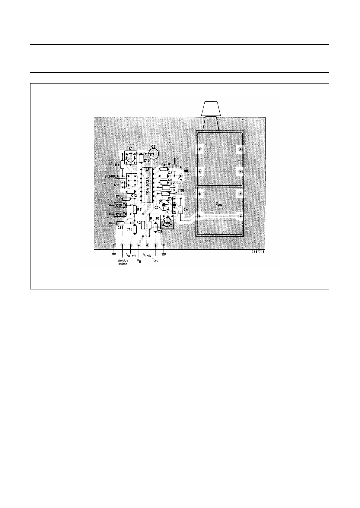
Fig.16 Printed-circuit board component side, showing component layout. For circuit diagram see Fig.1.
May 1984 16
Page 17
Philips Semiconductors Product specification
AM receiver circuit TDA1072A
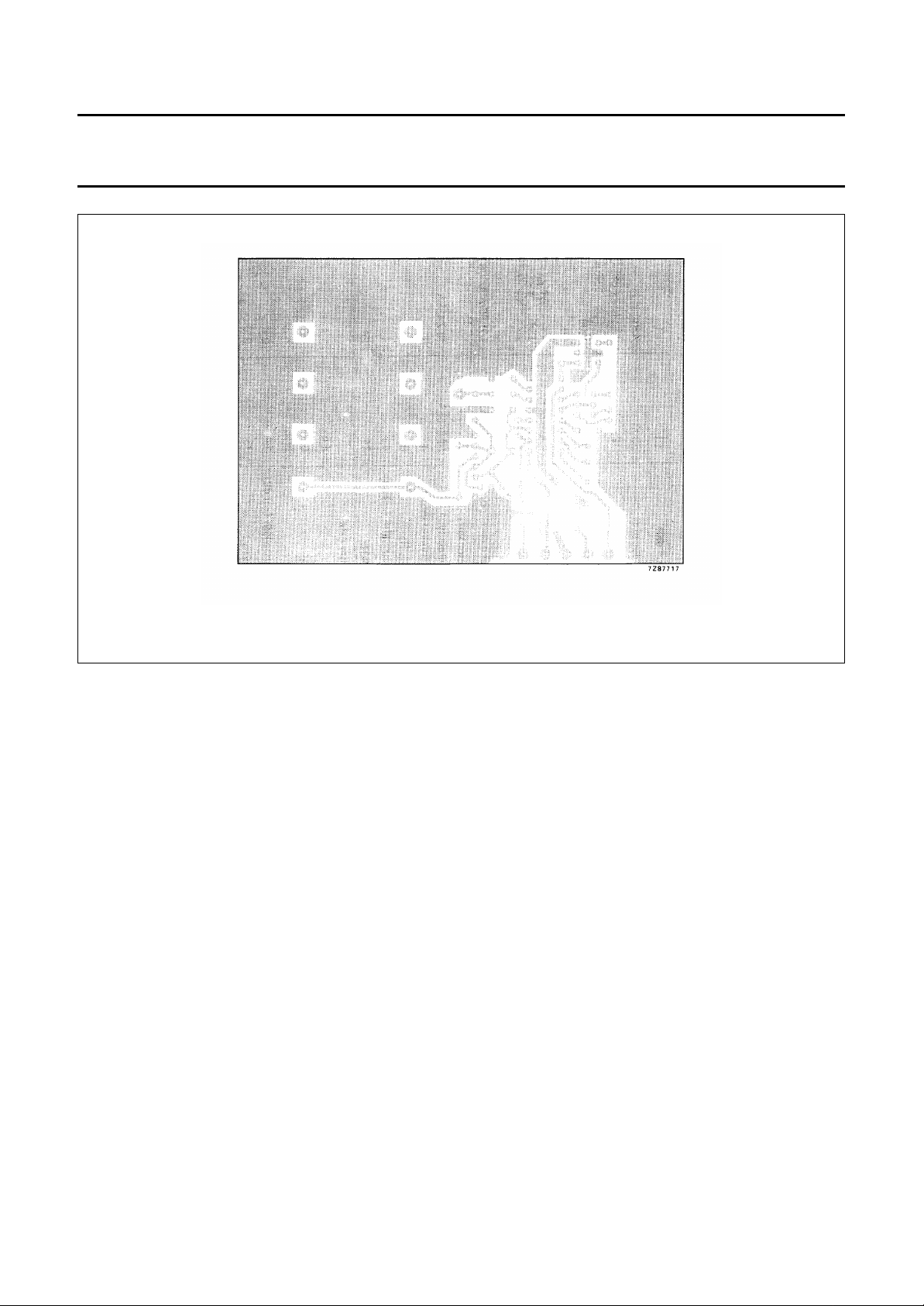
Fig.17 Printed-circuit board showing track side.
May 1984 17
Page 18
Philips Semiconductors Product specification
AM receiver circuit TDA1072A
May 1984 18
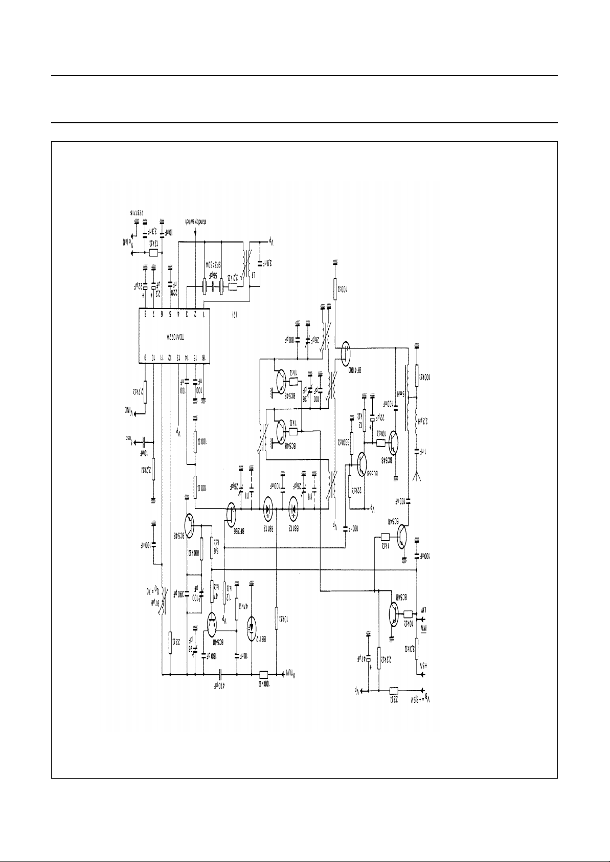
good large-signal handling.
(1) Values of capacitors depend on the selected group of capacitive diodes BB112.
Fig.18 Car radio application with capacitive diode tuning and electronic MW/LW switching. The circuit includes pre-stage a.g.c. optimized for
(2) For i.f. filter and coil data refer to Fig.1.
Page 19
Philips Semiconductors Product specification
AM receiver circuit TDA1072A
PACKAGE OUTLINE
DIP16: plastic dual in-line package; 16 leads (300 mil); long body
D
seating plane
L
Z
16
pin 1 index
e
b
b
1
9
A
1
w M
SOT38-1
M
E
A
2
A
c
(e )
1
M
H
E
1
0 5 10 mm
scale
DIMENSIONS (inch dimensions are derived from the original mm dimensions)
A
UNIT
mm
inches
Note
1. Plastic or metal protrusions of 0.25 mm maximum per side are not included.
A
max.
4.7 0.51 3.7
OUTLINE
VERSION
SOT38-1
min.
A
1 2
max.
0.15
IEC JEDEC EIAJ
050G09 MO-001AE
b
1.40
1.14
0.055
0.045
b
1
0.53
0.38
0.021
0.015
cEe M
0.32
0.23
0.013
0.009
REFERENCES
(1) (1)
D
21.8
21.4
0.86
0.84
May 1984 19
6.48
6.20
0.26
0.24
8
(1)
Z
e
0.30
1
0.15
0.13
M
L
3.9
3.4
E
8.25
7.80
0.32
0.31
EUROPEAN
PROJECTION
9.5
8.3
0.37
0.33
w
H
0.2542.54 7.62
0.010.100.0200.19
ISSUE DATE
92-10-02
95-01-19
max.
2.2
0.087
Page 20

Philips Semiconductors Product specification
AM receiver circuit TDA1072A
SOLDERING
Introduction
There is no soldering method that is ideal for all IC packages. Wave soldering is often preferred when through-hole and
surface mounted components are mixed on one printed-circuit board. However, wave soldering is not always suitable for
surface mounted ICs, or for printed-circuits with high population densities. In these situations reflow soldering is often
used.
This text gives a very brief insight to a complex technology. A more in-depth account of soldering ICs can be found in our
“IC Package Databook”
Soldering by dipping or by wave
The maximum permissible temperature of the solder is 260 °C; solder at this temperature must not be in contact with the
joint for more than 5 seconds. The total contact time of successive solder waves must not exceed 5 seconds.
The device may be mounted up to the seating plane, but the temperature of the plastic body must not exceed the
specified maximum storage temperature (T
be necessary immediately after soldering to keep the temperature within the permissible limit.
(order code 9398 652 90011).
). If the printed-circuit board has been pre-heated, forced cooling may
stg max
Repairing soldered joints
Apply a low voltage soldering iron (less than 24 V) to the lead(s) of the package, below the seating plane or not more
than 2 mm above it. If the temperature of the soldering iron bit is less than 300 °C it may remain in contact for up to
10 seconds. If the bit temperature is between 300 and 400 °C, contact may be up to 5 seconds.
DEFINITIONS
Data sheet status
Objective specification This data sheet contains target or goal specifications for product development.
Preliminary specification This data sheet contains preliminary data; supplementary data may be published later.
Product specification This data sheet contains final product specifications.
Limiting values
Limiting values given are in accordance with the Absolute Maximum Rating System (IEC 134). Stress above one or
more of the limiting values may cause permanent damage to the device. These are stress ratings only and operation
of the device at these or at any other conditions above those given in the Characteristics sections of the specification
is not implied. Exposure to limiting values for extended periods may affect device reliability.
Application information
Where application information is given, it is advisory and does not form part of the specification.
LIFE SUPPORT APPLICATIONS
These products are not designed for use in life support appliances, devices, or systems where malfunction of these
products can reasonably be expected to result in personal injury. Philips customers using or selling these products for
use in such applications do so at their own risk and agree to fully indemnify Philips for any damages resulting from such
improper use or sale.
May 1984 20
 Loading...