

Page 1

TECHNICAL NOTE
VERTICALDEFLECTION CIRCUITS FOR TV & MONITOR
By Alessandro MESSI
SUMMARY Page
1 INTRODUCTION. . . . . . . . . . . . . . . . . . . . . . . . . . ............................. 2
2 OSCILLATOR. . . ...................................................... 3
3 RAMP GENERATOR . . . . . . . . . . . . ....................................... 4
4 BLANKINGGENERATOR AND CRT PROTECTION. .......................... 4
5 POWERAMPLIFIERSTAGE . . . . . . . . . . . . . . . . . . . . . . . . . . ................... 4
6 THERMAL PROTECTION . . . . . . . . . . . . . . . . . . . . . .. . . . . . ................... 6
7 FLYBACKBEHAVIOUR . ................................................ 6
8 CURRENT- VOLTAGECHARACTERISTICSOF THE RECIRCULATING DIODES . . 11
9 CALCULATIONPROCEDURE OF THE FLYBACKDURATION . . . . . . . . . . . ....... 12
10 APPLICATIONINFORMATION . . ......................................... 12
11 SUPPLY VOLTAGECALCULATION . . . . . . . . . . . . . . . . .. . .. .. . . .. . . . . . . . . . . . . 14
12 CALCULATIONOF MIDPOINTAND GAIN . . . . .. . . . . . . . . . ................... 17
13 MONITOR APPLICATIONS . . . . . ......................................... 20
14 POWER DISSIPATION. . . . . . . . . .. . . . . . . . . . . ............................. 20
15 BLANKING PULSE DURATION ADJUSTMENT . . . . .. . ....................... 21
16 LINEARITY ADJUSTMENT. . ............................................. 21
17 FACILITIES AND IMPROVEMENTS . . . . . . . . . . . . . . . . . . . . ................... 22
18 GENERAL APPLICATION AND LAYOUT HINTS. ............................. 23
19 REFERENCES. . . . . ................................................... 23
AN373/0694
1/23
Page 2
VERTICALDEFLECTION CIRCUITS FOR TV & MONITOR
1 - INTRODUCTION
In a general way we can define vertical stages
circuits able to deliver a current ramp suitable to
drive the verticaldeflection yoke.
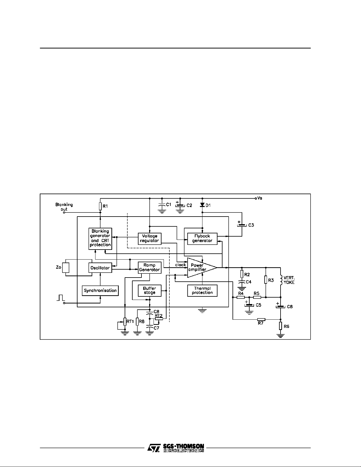
In Figure1 is representedthemore generalpossible blockdiagram of a deviceperformingthe vertical deflection.
Such a device will be called ”complete vertical
stage” because it can be simply driven by a synchronizationpulseand it comprises allthe circuitry
necessaryto performtheverticaldeflectionthatis:
oscillator, voltageramp generator,blanking gene-
tor, outputpower and flybackgenerator.
At the right side of the dotted line in Figure 1 is
represented the circuitry characterizing a ”vertical
output stage”. This kind of device comprises only
Figure 1 : BlockDiagram of a General Deflection Stage
the power stages and it has to be driven by a
voltage sawtooth generated by a previous circuit
(for examplea horizontaland verticalsynchronization stage.
In the first class there are the following devices :
TDA1170D, TDA1170N, TDA1170S, TDA1175,
TDA1670A, TDA1675, TDA1770A, TDA1872A,
TDA8176.
In thesecondclassthereare:TDA2170,TDA2270,
TDA8170, TDA8172, TDA8173, TDA8175,
TDA8178,TDA8179.
There is also a thrid class of vertical stages compraisingthevoltagerampgeneratorbutwithoutthe
oscillator; these circuits must be driven by an already synchronizedpulse. In this third class there
are : TDA1771and TDA8174.
2/23
AN373-01.EPS
Page 3
VERTICALDEFLECTION CIRCUITS FOR TV & MONITOR
2 - OSCILLATOR
There are two different kinds of oscillator stages
used in SGS-THOMSONcomplete verticaldeflections, one is used in TDA1170D, TDA1170N,
TDA1170S, TDA1175 and TDA8176, the other in
TDA1670A,TDA1675,TDA1170AandTDA1872A.
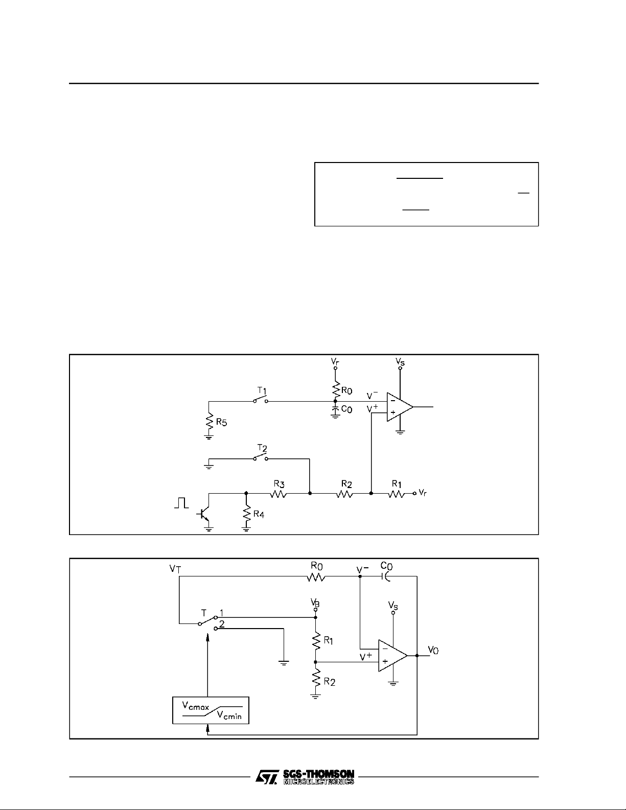
The principle of thefirst kind ofoscillator is represented in Figure2.
The followingexplanationswillbethemoregeneral
possible;we shall informthe readerwhenwe refer
to a particulardevice.
When the switchesT
capacitor charges exponentiallythrough ROto the
value V
tors R
+
(MAX)
1,R2,R3
determined by the integratedresis-
and R4. At this point the switches
are closed, short-circuitingR
age atthenon-invertinginputbecomesV
capacitor C
dischargesto this value through the
O
Figure 2 : First Kind of Oscillator Stage
and T2are opened the C
1
andR4, so the volt-
3
+
(MIN)
.The
integrated resistor R
.
5
The free running frequency can be easily calculated resultingin :
+
V
−V
R
TO= RO⋅ CO⋅ log
+ R5⋅ C
O
⋅log
VR− V
+
V
(MAX)
+
V
(MIN)
(MIN)
+
(MAX)
(1)
with RO= 360 kΩ and CO= 100 nF, it results in
43.7Hz.
O
Theoscillatorsynchronizationis obtainedreducing
the superior threshold V
resistor when a vertical synchronizationpulse
R
4
+
short-circuiting the
(MAX)
occurs.
The second kind of oscillator is represented in
Figure3.
1
f
=
O
T
O
Figure3 : Second Kind of OscillatorStage
AN373-02.EPS
AN373-03.EPS
3/23
Page 4

VERTICALDEFLECTION CIRCUITS FOR TV & MONITOR
When the switch T is in position 2, a constant
current I
with avoltageramp. When thevoltage V
V
O(MAX)
currentI
=V-/ROflows through COchargingit
CO
reaches
O
, T passes in position 1, so a constant
=(VB-V-)/ROdischargesthe capaci-
CO
tor causingthe inversionof the voltagerampslope
at the output V
reaches the value V
V
O
( t ). The dischargesstops when
O
and the cycle takes
O(MIN)
place again.
It ispossibletocalculatethe freerunningfrequency
withthe following formula :
f
O
TO=
with V
(V
+
O(MAX)
O(MAX)
( V
O(MAX)
− V
− V
-V
) ⋅ R
O(MIN)
−
V
O(MIN)
VB− V
O(MIN)
O⋅CO
) ⋅ R
⋅ C
O
−
O
= 3.9V, VB= 6.5V, V
(2)
= 0.445V,RO= 7.5kΩ and CO= 330nF it results
= 43.8Hz.
in : f
O
Theoscillatorsynchronizationisstill obtainedinthe
above mentioned way.
In order to guarantee a minimum pull-in range of
14Hz the threshold value has been chosen in
= 4.3V.
V
P
The spread of the free running frequency in this
kind of oscillator is very low because it mainly
dependsfromthethresholdvaluesV
O(MAX),VO(MIN)
and V-that are determinedby resistor rates that
can be done very precise.
3 - RAMP GENERATOR
The rampgeneratoris conceptuallyrepresentedin
Figure 4.
The Voltage ramp is obtained charging the group
R
Itiseasy tocalculatethevoltageV
and C2with a constant current IX.
1,C1
RAMP
Thatresults
in :
1
V
RAMP
where V
(t)=(V
(MIN)
− R1⋅ IX) e
(MIN)
is the voltage in A when the charge
−
starts and Cis the seriesof C
TheresistorR
isnecessarytogivea ”C correction”
1
⋅ C
R
1
and C2.
1
+ R1⋅ I
(3)
X
to the voltage ramp. Theramp amplitude is determined by I
X=VREG/P1
,sothe potentiometerP1is
necessaryto perform the height control.
The voltage ramp is then transferred on a low
impedencein B througha bufferstage.
TheP2 potentiometerconnectedbetweenD andB
performstheramplinearitycontrolor”Scorrection”
that is necessaryto havea correct reproductionof
the imageson the TV set.
The voltage ramp in B grows upuntil the switch T
is closedby a clockpulse coming from the oscillator; in this way the capacitors discharge fastly to
that is dependent upon the saturation volt-
V
(MIN)
age of the transistor thatrealizes the switch.
At this point the exponential charge takes place
again.
4 - BLANKING GENERATOR AND CRT PROTECTION
-
This circuit senses the presenceof theclockpulse
coming from the oscillator stage and the flyback
pulse on the yoke. If both of them are present a
blankingpulse is generatedable to blank the CRT
duringthe retraceperiod.Thedurationof thispulse
is the same of the one coming from the oscillator.
If for any reason the verticaldeflection would fail,
for instance for a short circuit or an open circuitof
the yoke,theabsenceof theflybackpulse puts the
circuitinsuch a condition thata continuousvertical
blanking is generated in order to protect the CRT
againsteventual damages.
This circuit is available only in the following devices :TDA1670A, TDA1675, TDA1770A and
TDA1872A.
The stages we will consider startingfrom this point
are common both to complete vertical stages and
verticaloutput stages.
5 - POWERAMPLIFIER STAGE
This stage can be divided into two distinct parts :
the amplifiercircuitand the output power.
The amplifieris realizedwith a differentialcircuit; a
schematicdiagram is representedin Figure 5.
The open-loop gain of the circuit is variable from
60dB to 90dBfor the different integratedcircuits.
The compensation capacitor C determines the
dominantpole ofthe amplifier. In orderto obtain a
dominantpolein the rangeof 400Hz,thecapacitor
must be of about 10pF.
1
4/23
Page 5
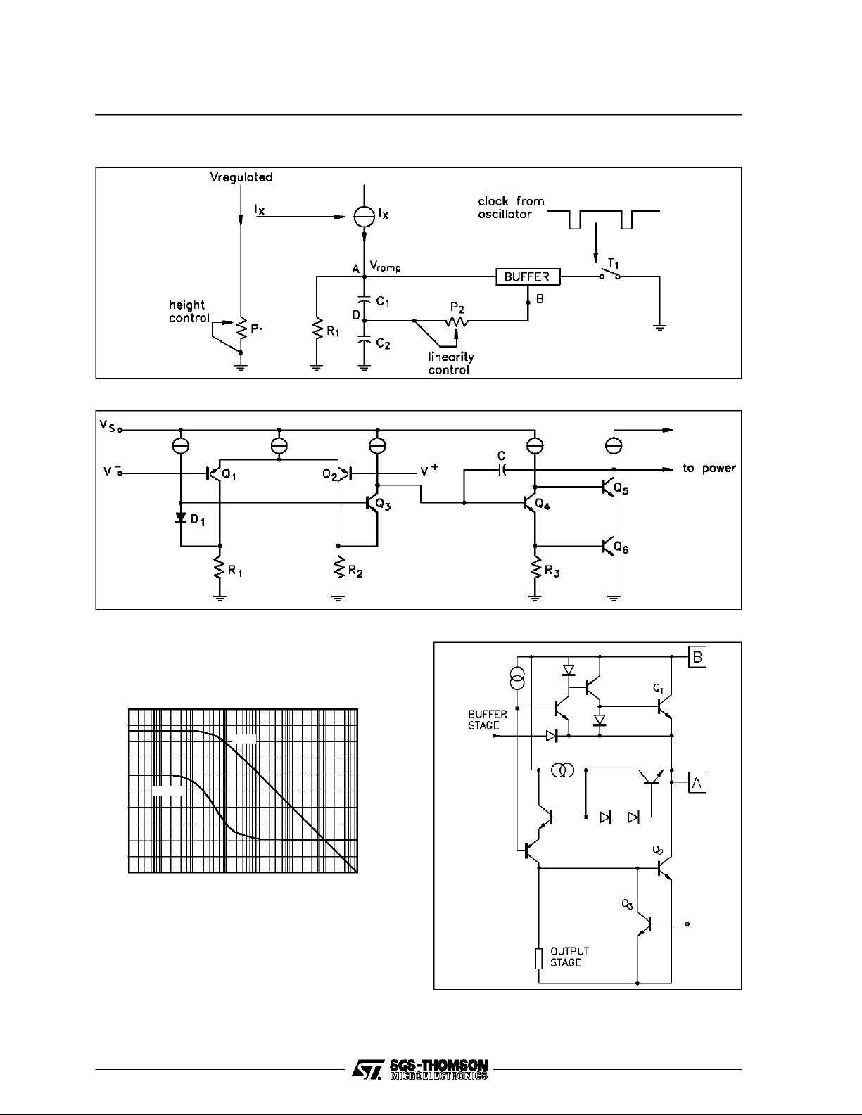
Figure4 : Ramp Generator
Figure5 : AmplifierStage
VERTICALDEFLECTION CIRCUITS FOR TV & MONITOR
AN373-04.EPS
As an examplein Figure 6 is representedtheboole
diagram of the amplifier open loop gain for
TDA8172.
Figure 6 : AmplifierOpen Loop Gainand Phase
6
90
45
0
-45
-90
- 135
7
100
80
60
PHASE
GAIN(dB)
40
20
0
1 1010101010 1010
GAIN
23
FREQUENCY, f (Hz)
4
5
The output power stage is designed in order to
delivertotheyokeaverticaldeflectioncurrentfrom
1 to2Apeak,dependinguponthedifferentdevices,
and able to support flyback voltages up to 60V. A
typical output stage is depictedin Figure 7.
AN373-05.EPS
Figure7 : Power Stage
PHASE (Degrees)
AN373-06.EPS
AN373-07.EPS
5/23
Page 6
VERTICALDEFLECTION CIRCUITS FOR TV & MONITOR
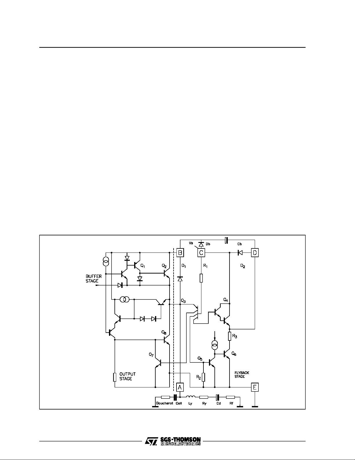
The upperpowertransistorQ
conductsduringthe
1
first part of the scanning period when the vertical
deflectioncurrentisflowingfromthesupplyvoltage
into theyoke;whenthecurrent becomesnegative,
that isit comesout of the yoke,it flows throughthe
lower power transistor Q
.The circuit connected
2
between the two output transistorsis necessaryto
avoid distortion of the current at the crossing of
zero, when Q
When the flybackbegins, Q
is turned off and Q2isturned on.
1
isswitched-offby Q
2
in order to makeit ableto support the highvoltage
of the flyback pulse.
The circuitbehaviourduring flybackis explainedin
chapter 7.
6 - THERMALPROTECTION
Thethermalprotectionisavailableinallthe devices
except theTDA1170 family andthe TDA8176.
This circuit is usefull to avoid damages at the
integrated circuit due to a too high junction temperaturecausedby an incorrectworkingcondition.
It is possible to sense the silicon temperature because the transistorV
varies of - 2 mV/oC, so a
BE
Figure8 : Output Power and FlybackStages
temperature variation can be reconducted to a
voltagevariation.
If the temperature increases and it is reaching
o
C, theintegratedcircuit output isshut downby
150
puttingoff the current sources of the power stage.
7 - FLYBACK BEHAVIOUR
In orderto obtain sufficiently short flyback times,a
3
voltage greather than the scanning voltage must
be appliedto the deflection yoke.
By using a flyback generator, the yoke is only
supplied with a voltage close to double the supply
during flyback.
Thus, the power dissipated is reduced to approximately one thirdand the flyback time is halfed.
The flyback circuit is shown in Figure 8 together
with the powerstage.
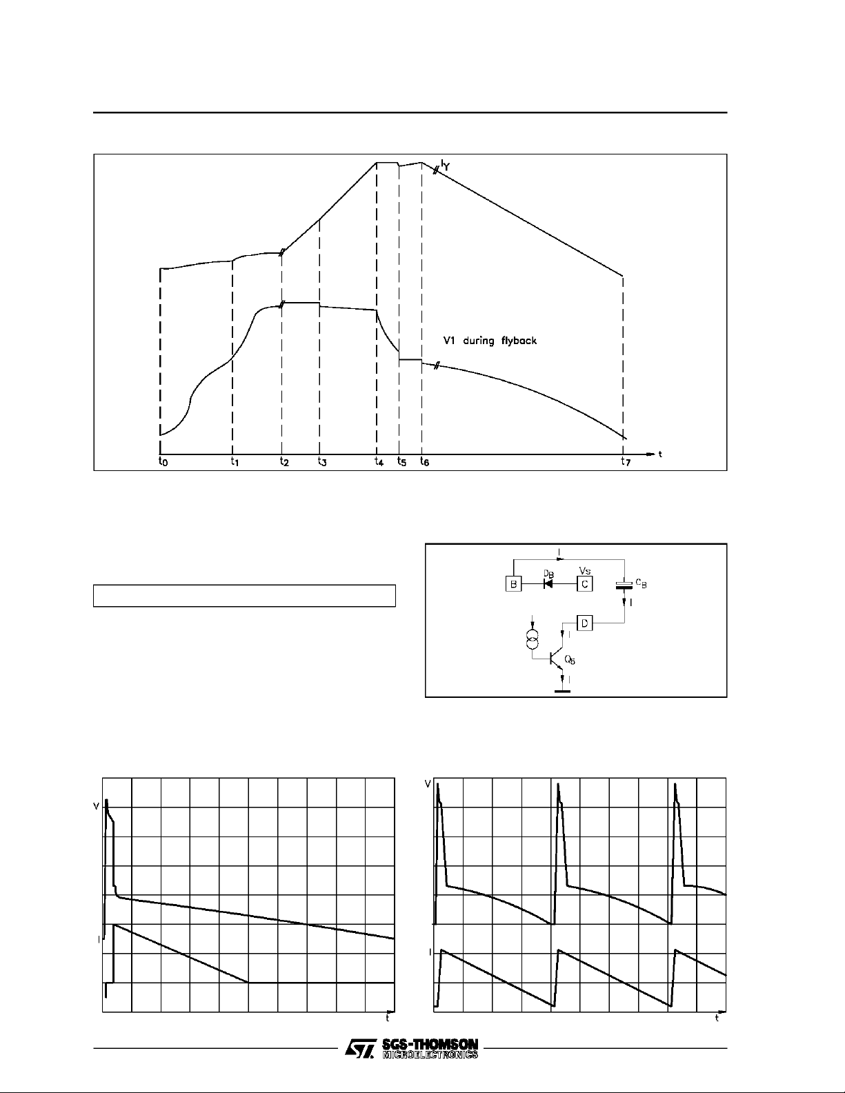
Figure 9 showsthe circuit behaviuor, to show operation clearly. Thegraphsare not drawnto scale.
Certainapproximationsare made in the analysisin
order to eliminate electrical parametersthatdo not
significantlyinfluence circuit operations.
6/23
AN373-08.EPS
Page 7
VERTICALDEFLECTION CIRCUITS FOR TV & MONITOR
Figure9 : Current in theYokeand VoltageDrop on The Yoke during VerticalDeflection
AN373-09.EPS
a) Scan period (t
During scanning Q
causes Q
to saturate.
6
):Figure10
6-t7
3,Q4
and Q5are off and this
A current from the voltage supply to ground flows
through D
and Q6charging the CBcapacitor
B,CB
up to :
VCB=VS-VDB-VQ
6SAT
(4)
At the end of this period the scan current has
reacheditspeakvalue (I
yoke to the device. At the same time V
) andit is flowingfromthe
P
A
has
reached its minimum value.
In Figures11 and 12are depictedthe voltagedrop
Figure 11 : Voltage Drop on the Yoke and Cur-
rent Flowingthrough D
B
V = 10V/div. - I = 0.5A/div.
t = 2ms/div.
on the yoke and the currents flowing through D
and the yoke.
Figure10 : Circuit involvedduring Scan Period
Figure12 : Voltage Drop on the Yoke and Cur-
rent Flowingthroughthe Yoke
V = 10V/div. - I = 1A/div.
t = 5ms/div.
B
AN373-10.EPS
AN373-11.EPS
AN373-12.EPS
7/23
Page 8
VERTICALDEFLECTION CIRCUITS FOR TV & MONITOR
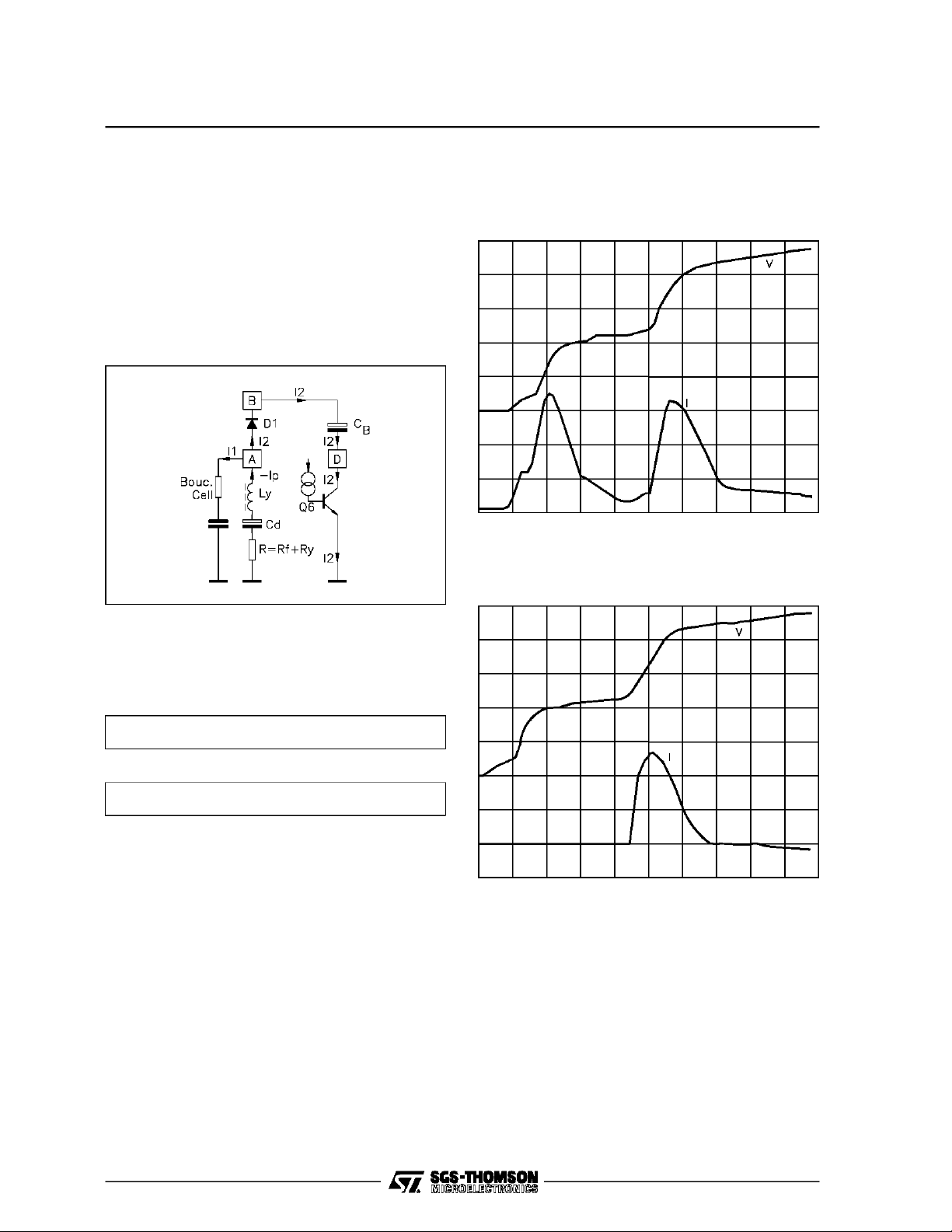
b) Flyback starting (t
Q
, that was conductingthe - IPcurrent, is turned
8
):Figure13
0-t1
off by the bufferstage.
The yoke, charged to I
flow partially through the Boucherot cell (I
partially through D
, now forcesthis current to
P
and Q6(I2).
1,CB
) and
1
In Figures 14, 15 and 16 are represented the
currents flowing through the yoke, the Boucherot
cell and D1.
Figure13:CircuitinvolvedduringFlybackStarting
c) Flyback starting (t
When the voltage drop at pin A rises over V
1-t2
)
S,Q3
turns on and this causes Q4and Q5to saturate.
ConsequentlyQ
turnsoff.
6
During this period the voltageat pinD is forcedto :
Figure14 : Voltage Drop on the Yoke and Cur-
rent Flowingthroughthe Boucherot
Cell- V = 10V/div.
I = 1A/div. - t = 1µs/div.
Figure15 : Voltage Drop on the Yoke and Cur-
rent FlowingthroughD
1
V = 10V/div. - I = 1A/div.
AN373-13.EPS
t=1µs/div.
AN373-14.EPS
VD=VS-VQ
4SAT
(5)
Therefore the voltage at pinB becomes :
VB=VCB+V
D
(6)
The yokecurrent flowsintheBoucherotcelladded
to anothercurrentpeakflowingfrom V
(Figures14 and 15).
C
B
8/23
viaQ4and
S
AN373-15.EPS
Page 9

VERTICALDEFLECTION CIRCUITS FOR TV & MONITOR
Figure 16 : Voltage Drop on the Yoke and Cur-
rent Flowingthrough the Yoke
V = 10V/div. - I = 100mA/div.
t=1µs/div.
d) Negativecurrent rise(t
):Figure 17
2-t3
Figure 17 : Circuit involved duringthe Negative
CurrentRise
2
R
d
i
di
+
2
L
Y
dt
1
+
dt
L
YCD
i= 0
it resultsin :
I
P
(−α +β) t
i(t)
=
-
2β∆T
e
1 − e
1
I
P
−2β∆T
− 1
e
e
1
(−α−β)t
where :
α =
R
2L
β=√
Y
4 ⋅ L
R
Y
1
−
2
L
Y
C
D
∆T1=t3-t
2
Becauseof ∆T1 is two orders of magnitudelower
than the scan time, we can apply an exponential
sum to obtainthe followingequation :
AN373-16.EPS
α cosh
i(t)=
(2β∆T1)+ βsinh (2β∆T
cosh(2β∆T
)−1
1
)−α
1
t−I
P
Simplifying:
1
i(t)= I
α+
P
∆T
t−I
P (12)
1
(9)
(10)
2
(11)
During this period, thevoltage applied at pinA is :
VA=VB+VD1,
V
A=VCB+VD+VD1
V
A=VS-VDB
=2.VS+VD1+VD2-VDB-VQ
V
A
,
-VQ
6SAT+VS+VD2+VD1
6SAT
,
(7)
It is possible to calculate the current solving the
followingequation :
di
Y
+ R
1
i ⋅ dt + R ⋅ i
+
dt
∫
C
D
Y
(8)
V
= L
A
where R = R
F
Because the voltage at pin A is approximatively
constant (error less than 2%) we can simplify the
(8) in the following equation:
The slopeof thecurrentis therefore :
R
di
=
2
dt
1
∆T
I
(A/s)
P
1
+
L
Y
The currentflows from the yoke to VSthrough D1,
andD2, and it is depicted in Figure18.
C
B
Figure18 : Voltage Drop on the Yoke and Cur-
rent Flowingthroughthe Yoke
AN373-17.EPS
V = 10V/div. - I = 250mA/div.
t = 100µs/div.
(13)
AN373-18.EPS
9/23
Page 10

VERTICALDEFLECTION CIRCUITS FOR TV & MONITOR
e) Positive current rise (t3-t4):Figure19
Figure 19 : Circuit involved duringthe Positive
CurrentRise
When the current becomes zero, D
saturates; so the pin Avoltage becames :
Q
2
VA=VB-VQ
VA=2.VS-VDB-VQ
2SAT
6SAT
-VQ
4SAT
turns off and
1
-VQ
2SAT
(14)
The current flows from +VSinto the yoke through
Q
and Q2and rises from zero to IPas it can
4,CB
be seen in Figure18.
By usingthe previousprocedure explained in sec-
tion d), we can obtain the slopeof the current :
Figure20 : VoltageDrop on the Yoke and Cur-
rentFlowingthrough C
B
V = 10V/div.- I = 0.5mA/div.
t = 100µs/div.
AN373-19.EPS
Figure21 : Voltage Drop on the Yoke and Cur-
rent Flowingthroughthe Boucherot
Cell- V = 10V/div.
I = 100mA/div. - t =100µs/div.
AN373-20.EPS
R
di
=
2
dt
where ∆T2= t4− t
1
+
L
Y
I
(A/s)
P
∆T
2
3
f) Flyback decay (t4-t5)
Whenthe yokecurrentreachesits maximum peak,
Q
desaturates and conducts the maximum peak
2
current flowing from V
currentflowingthroughC
via Q4and CBinto LY; the
S
isdepictedin Figure20.
B
AN373-21.EPS
10/23
Page 11
VERTICALDEFLECTION CIRCUITS FOR TV & MONITOR
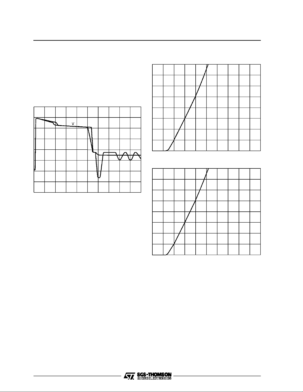
An eventualantiringing parallelresistor modifythe
linear decay slopein an exponentialone, as it can
be seen in Figure22.
This continuesuntil the buffer stage turns Q
on.
2
The effectof theBoucherotcell during thisperiode
is negligible(see Figure21).
Figure 22 : Effect of Resistorin Parallelcon-
nected to the Yoke
V = 10V/div.
g) V
pedestal(t5-t6)
A
When V
reaches the value VSof the supply volt-
A
age, the flyback generatorstops its function.
is turned off and turns off Q4that open the
Q
3
connection between pin D and V
Therefore V
= VS− VDB− VQ
V
A
drops to VS-VDBwhile :
B
2CE on
.
S
At this point the normal scan takes place.
Figure23 : I-V Characteristicsof the Diode D
V = 500mV/div.- I =200mA/div.
Figure24 : I-V Characteristicsof the Diode D
V = 500mV/div.- I =200mA/div.
AN373-22.EPS
1
AN373-23.EPS
2
8 - CURRENT-VOLTAGE CHARACTERISTICS
OF THE RECIRCULATING DIODES
The followingFigures 23 and 24 reproduce the I-V
characteristics of the integrated recirculating diodes D
and D2(see Figure8)
1
AN373-24.EPS
These characteristics are useful in order to calculatethe maximumvoltagereachedat pin Awith the
formula(7) explained in chapter 7.
11/23
Page 12

VERTICALDEFLECTION CIRCUITS FOR TV & MONITOR
9 - CALCULATION PROCEDURE OF THE FLYBACK DURATION
The flyback duration can be calculated using the
followingprocedure (referring to Figure25).
Figure25 : Circuit involved in the Calculation of
FlybackDuration
During the flyback period the voltage applied at
pin A is about 2 V
chapter 7. The voltage drop across C
matively a constant voltage little less than V
The voltageon the feedbackresistor R
VR
(t)= RFIY(t)
F
, as previously explained in
S
isapproxi-
D
S
is :
F
/2.
so in the period which we are considering it is
negligible respect to V
/2.
S
The effect of the Boucherotcell during this period
is notsensibleas it can be seenin Figure 21;while
R
acts principally during the flyback decay time
D
(Figure9 : t
) reducingitsslopeandthe resulting
4-t5
oscillations but doesn’t influence the total flyback
time asshownin Figure 22. Sotheirinfluencesare
also negligible.
Now theeffectivevoltage drop acrosstheyokecan
be approximated to :
V
3
S
=
2 ⋅ VS−
V
2
S
2
Figure 25 can be simplified as shown in Figure26.
Figure 26 : Simplified Circuit for the Calculation
of FlybackDuration
The voltage charges the coil with a linear current
that can be calculatedin the following way :
i(t)=
i(t)=
1
V⋅dt =
∫
L
Y
3
1
2
L
Y
V
⋅t+K
S
1
3
⋅ dt
V
S
∫
L
2
Y
K is calculated imposing that the current at the
beginningof the flybackis -I
i(0) = - I
3
i(t) =
2
K=-I
P
V
S
t − I
L
Y
P
P
.
P
At theend of the flyback period the currentwill be
, so we can write :
+I
P
V
3
S
=
P
tF− I
L
2
P
Y
AN373-25.EPS
I
Theduration of the flyback period is then :
I
4
PLY
t
=
F
V
3
IYL
2
Y
=
3
S
V
S
10 - APPLICATIONINFORMATION
Thevertical deflection stages productedby SGSTHOMSON are able to cover the complete range
ofapplicationsthat the market need for color televisionand high/veryhigh resolution monitors.
Television and monitor applications are not very
different but in monitor field, in addition to the
linearityand interlacing problems, we have to pay
attentiontotheflybacktimethat mustbe veryshort
for very high resolutionmodels.
In television applications the most important requirement is to choose the lowest supply voltage
possiblein orderto minimizethe powerdissipation
in the integrated circuit, reducingthe dimensionof
the heatsink, and the power dissipation from the
voltagesupplier.
These results can be reached very easily with
SGS-THOMSONdeflectionstagesbecauseof the
highefficiencyoftheflyback generatorcircuitused.
In high resolution monitors one of the main problems is to reach the very short flyback time requested; the flyback generator, together with the
high current and power dissipation capabilities,
solveall the problemsin a simple way.
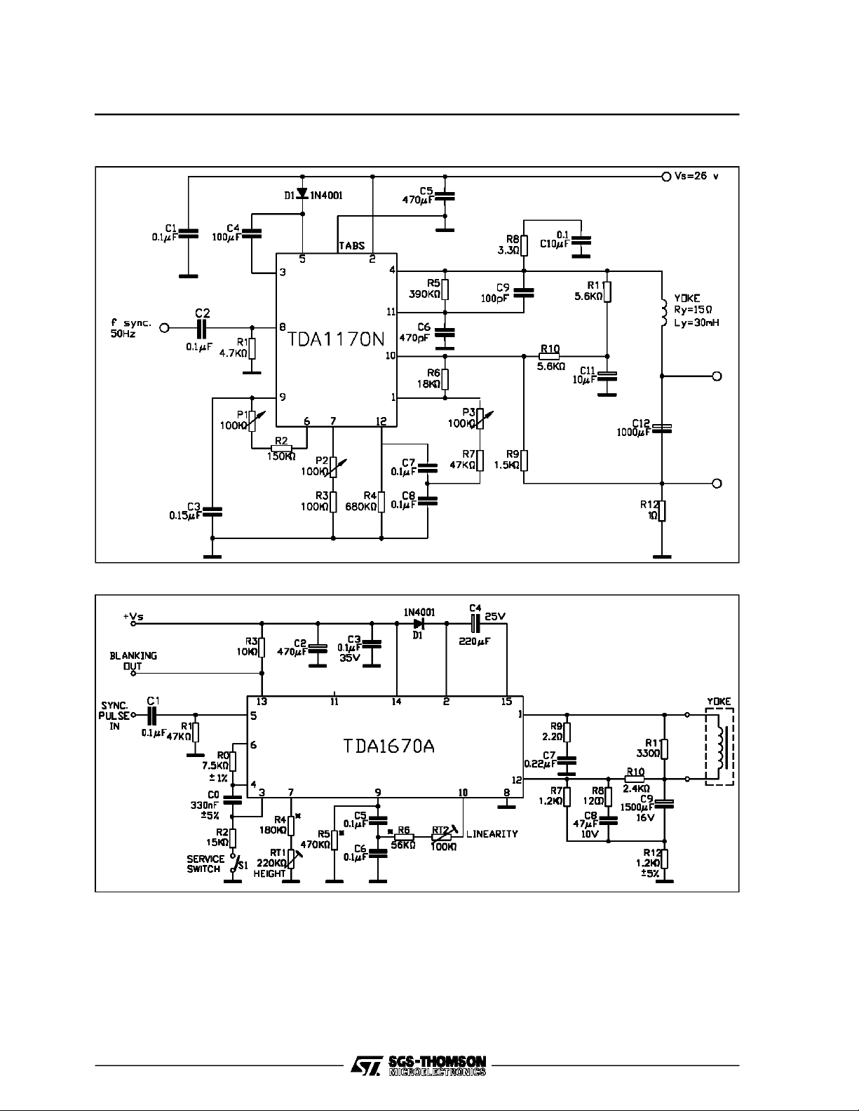
In Figures 27,28 and 29 are depicted threetypical
application circuits for the different kinds of inte-
AN373-26.EPS
gratedcircuits available.
(16)
(17)
(18)
12/23
Page 13
VERTICALDEFLECTION CIRCUITS FOR TV & MONITOR
Figure27 : ApplicationCircuitforTDA1170
Figure 28 : ApplicationCircuitfor TDA1670A
In the following chapterswe shall dothe calculationfor televisionand monitor inorder to choosethe right
voltage supply and externalnetwork for the yoke used and the currentrequirements.
AN37-27.EPS
AN37-28.EPS
13/23
Page 14
VERTICALDEFLECTION CIRCUITS FOR TV & MONITOR
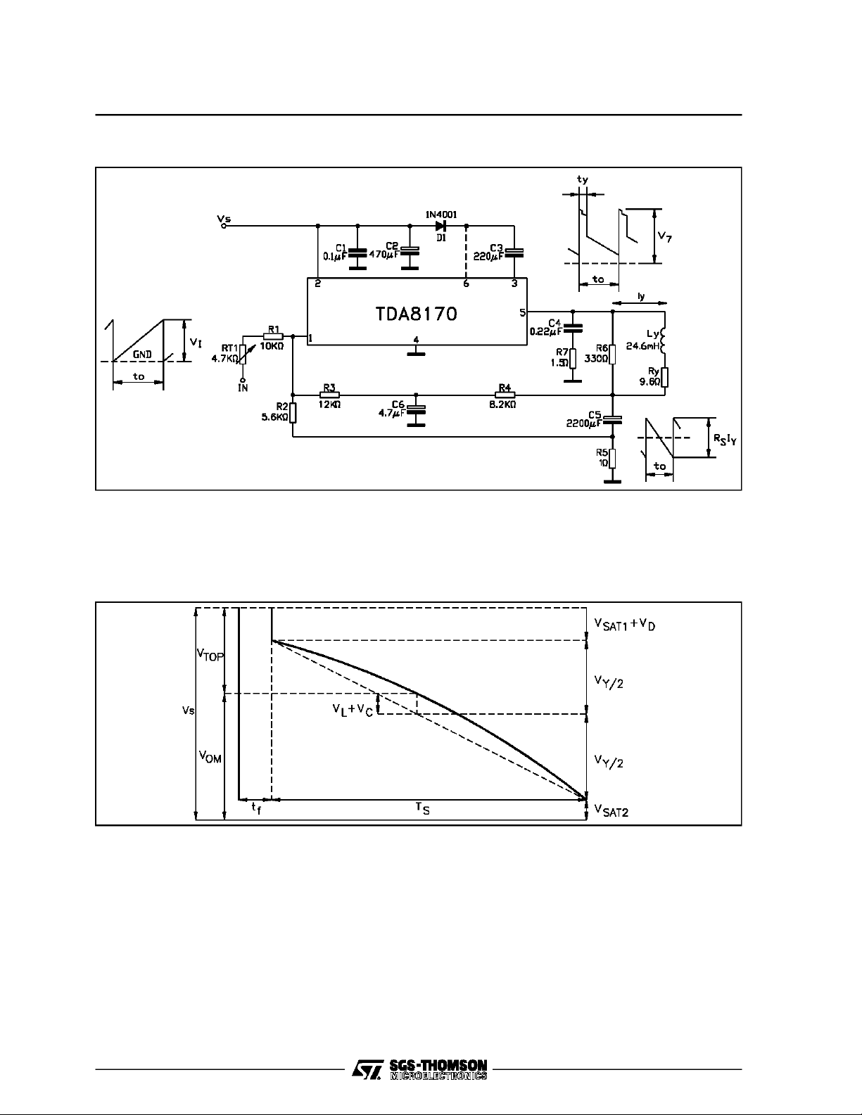
Figure 29 : ApplicationCircuitfor TDA8170
11 - SUPPLY VOLTAGECALCULATION
current required for thegiven application.
AN37-29.EPS
For television applications we shall calculate the
minimumsupplyvoltagenecessarytohavevertical
scanning knowingthe yoke characteristicsand the
Figure 30 shows the terms used in this section,
while the circuit part involved in the following calculationsis depictedin Figure31.
Figure 30 : Parametersused in theCalculation of the Supply Voltage
AN373-30.EPS
14/23
Page 15
VERTICALDEFLECTION CIRCUITS FOR TV & MONITOR
Figure 31 : Circuit involved in the Calculation of
the SupplyVoltage
V
V
= supply voltage
S
= nominal voltagerequiredto produce the
Y
scanningcurrentincludingthe feedback
resistance and the 20% increasing for
temperature variations in the yoke
current
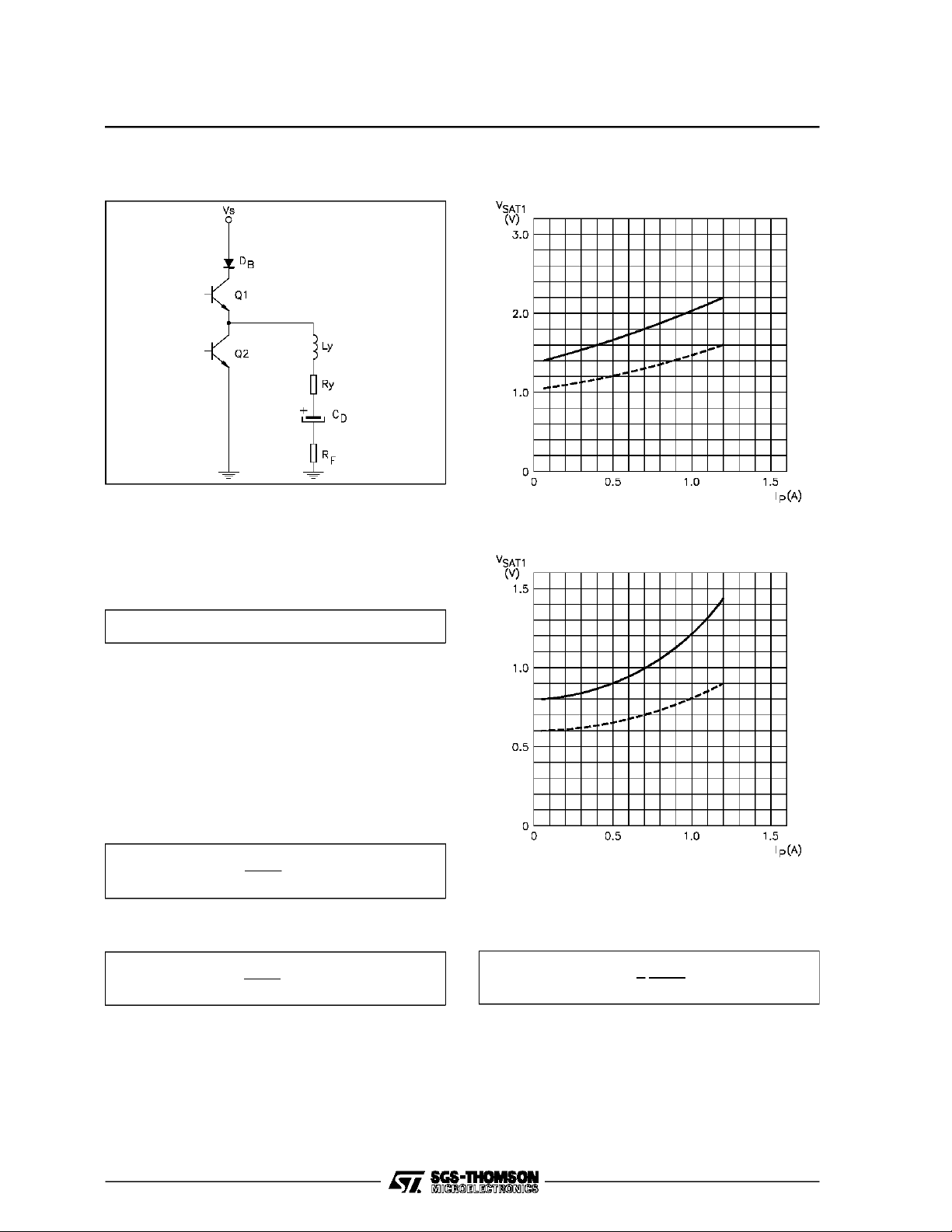
Figure32 : Saturation Characteristicof the
UpperPower Transistor
AN373-31.EPS
AN373-32.EPS
Figure33 : Saturation Characteristicof the
LowerPower Transistor
V
V
V
V
V
VY= (1.2 RY+RF)I
= nominaloutputsaturationvoltagedue to
SAT1
Y
the upper power transistorQ
(see Figure 32);
= nominaloutputsaturationvoltagedue to
SAT2
the lower power transistor Q
(see Figure 33)
= nominalquiescentvoltage (midpoint)on
OM
the output power transistors
= voltage peak due to the charge of C
C
capacitor
IY⋅ t
=
=
8 ⋅ C
LY⋅ I
t
S
S
D
Y
Y
V
C
= voltage drop due to the yoke
L
inductanceL
V
L
(19)
1
2
D
AN373-33.EPS
(20)
V
= nominal voltage drop on DBdiode in
D
serieswith the supply
T = verticalscanperiod
t
(21)
= flyback time
F
I
⋅ L
2
Y
t
=
F
Y
V
3
S
15/23
Page 16

VERTICALDEFLECTION CIRCUITS FOR TV & MONITOR
t
I
R
L
R
= scanning time
S
tS=T-t
= peak-to-peakdeflectioncurrent
Y
= nominal yoke resistance
Y
= nominal yoke inductance
Y
= feedbakresistor
F
F
Referring to Figure 30 it is easy to see that the
minimumsupply voltage is given by
VS=VOM+V
TOP
(22)
where :
V
Y
VOM=
+ V
+ V
SAT2
2
+ V
C
L
(23)
and :
V
Y
V
TOP
+ V
=
2
+ V
D
SAT1
− V
− V
L
C
(24)
So we obtain :
VS=VY+VD+V
SAT1+VSAT2
(25)
The (25) gives the minimum voltage supply if we
do not consider the tolerances of the integrated
circuit and of the external components, but the
calculation,evenif it was not realistic, it wasuseful
in order to understand the procedure.
Now we shall dothe same thingconsideringall the
possiblespreads;wecaninthisway obtainthereal
minimumsupply voltage.
We shall follow the statistical composition of
spreadsbecauseitisneverpossiblethatall ofthem
are presentat thesame time with the same sign.
We must considerthe following spreads :
● ∆V
due to the variationof yoke and feedback
Y
resistance and yoke current, supposing a
10% of regulation range in scanning
currentandaprecisionof7% forresistors;
∆VY= (1.2 RY+RF) 1.07 (1.1 IY)-V
● ∆V
due tothetoleranceofCDandyokecurrent
C
Y
(26)
regulation;
1.1I
∆V
C
YtS
=
8C
D(min)
− V
C
(27)
● ∆V
duetothetoleranceofLY(±10%)andyoke
L
current regulation;
1.1 I
1.1 L
Y
∆V
=
L
∆V
SAT1=VSAT1(MAX)-VSAT1
∆V
SAT2=VSAT2(MAX)-VSAT2
Y
− V
t
S
L
(28)
Foreachparameter,itisnecessaryto calculatethe
factor p, expressing the percentual influence of
every parameter variation on the nominal supply
voltage,with the followingformulas:
OM
TOP
:
∆V
ρ =
V
OM
:
∆V
ρ =
V
TOP
for V
for V
Wehave then tocalculatethe squaremean rootof
the spreadsexpressedas :
2
√ Σ ρ
So if wecall :
V
OM1
= V
OM
1
+ √ Σρ
2
and :
V
TOP1
= V
TOP
1+
√ Σρ
2
Wecan write :
VS=V
OM1+VTOP1
(29)
An example of calculation will better explain the
procedure. We shall consider a 26”, 110
neck29.1mm tube whosecharacteristicsare :
I
=1.2 App,
Y
= 9.6Ω ± 7%,
R
Y
=24.6mH ± 10%.
L
Y
Weshall usea couplingcapacitanceC
of1500µF
D
with + 50% and - 10% tolerance and a feedback
resistanceR
of 1.2Ω.
F
o
,
16/23
Page 17

VERTICALDEFLECTION CIRCUITS FOR TV & MONITOR
a) Nominal minimum supply voltage:
VY= (1.2 RY+RF)I
I
⋅ t
Y
V
V
V
V
V
C
L
SAT1
D
OM
S
=
=
8 ⋅ C
L
Y⋅IY
t
D
S
=2V
= 1.476V
= 1.25V V
=1V
= 11.788V V
= 15.264V
Y
= 0.68V
SAT2
= 6.406V
TOP
We obtain: VS=18.2V
b) Statisticalminimum supply voltage:
∆VC= 2.702V
V
Y
⁄
ρ V
YM
ρ VYT=
2
=
V
OM
V
Y
⁄
2
V
TOP
ρ2VYM= 1.313 . 10
ρ2VYT= 4.447 . 10
∆VC= 0.445V ρ2VCM= 1.421 . 10
ρ2VCT= 4.813 . 10
∆VL= 0.31V ρ2VLM= 6.914 . 10
ρ2VLT= 2.341 . 10
∆V
= 0.45V ρ2V
SAT1
∆V
= 0.27V ρ2V
SAT2
V
OM1=VOM
V
TOP1=VTOP
V
S=VOM1+VTOP1
( 1+ √ Σρ2)= 13.268V
( 1 + √ Σρ2)= 7.930V
= 21.2V
SAT1T
SAT2T
= 4.935. 10
= 5.246. 10
-3
-3
-3
-3
-4
-3
-3
-4
This isareal value for the minimumsupplyvoltage
needed by the above mentionedapplication.
In this case we obtain a flybackdurationof about :
TDA11 75, TDA21 70, TDA2270, TDA8170,
TDA8172,TDA8173,TDA8175and TDA8176.
Theequivalent circuit of the output stage is representedin Figure 34.
Figure34 : Circuit utilized for the calculationof
Midpointand Gain for TDA1170,
TDA1175,TDA8176,TDA2170,
TDA2270,TDA8170,TDA8172,
TDA8173and TDA8175
For DC considerations we shall consider the two
capacitors as open circuits. Because of the very
high gainof the amplifierwe can suppose:
−
= VR.
V
We can so write :
I1+I2=I
3
(30)
AN373-34.EPS
IY⋅ L
2
tF=
Y
V
S
≈ 900µs
3
12 - CALCULATION OF MIDPOINTANDGAIN
For the calculation of the output midpoint voltage,
it is necessary to consider the different feedback
network for the applications of the various integrated circuits.
We shall first consider the TDA1170 family, the
where :
I1=
V
− V
i
R
R
1
I2=
V
− V
O
RA+ R
R
B
Substitutinginto the (30) we obtain :
VO= V
RA+ R
1 +
R
R
B
−(V
+R
F
S
i−VR
(R
)
I3=
RF+ R
A+RB
R
1
V
R
S
(31)
17/23
Page 18

VERTICALDEFLECTION CIRCUITS FOR TV & MONITOR
Let’s consider now TDA1670A, TDA1675,
TDA1770A, TDA1771, TDA1872A and TDA8174.
The equivalent output circuit is depicted in Figure 35.
Figure 35 : Circuit utilized for the calculationof
Midpoint and Gain for TDA1670A,
TDA1675,TDA1770A,TDA1771,
TDA1872Aand TDA8174
We can write :
I1=I
2
I
2+I3=I4
(32)
(33)
where :
I1=
V
− V
i
R
R
1
I2=
V
R−VX
R
V
− V
O
I3=
2
X
R
A
I4=
V
X
RB+ R
S
wth the (32) and (33) we can calculate the DC
output voltage. It resultsin :
VO=V
-V
R
i
RA+R
1+
RA+R
R
1
R
R
2
A(R1+R2
+
R
1
2
1(RB+RS
RA⋅R
+
R1(RB+RS)
)
)
2
Referring to Figures 34 and 35, it is possible to
calculatethe transconductancegain of the power
amplifier. Forthiscalculationweshalldo thefollowing approximations:
- the capacitorsare practicallyshort circuits;
- the gainA of theamplifieris veryhigh (A→
Forthe circuit representedin Figure 34we obtain :
R
Y
=
F
R1⋅ R
V
i
S
I
while for the application in Figure 35 the koke
currentresults in :
R
+ RA// RB//R
AN373-35.EPS
2
I
=
Y
R1⋅ R
C
V
S
i
Using the (31), (34), (35) and (36) it is possible to
calculate the external feedbacknetwork for every
differentyoke known the scanningcurrent and the
midpointouput voltage.
We can now consider the open loop gain of the
wholesystemamplifierplusexternalfeedbacknetwork.Thiscalculationisusefulin ordertoverifythat
no oscillations can occur at any frequency.
We shall consider some typical applications; the
resultsare reported in Figures36, 37 and 38.
It is easy to verify that in all cases, when the gain
reaches0dB,the phasemarginisabout60
o
stabilityof the system is assured.
(34)
∞).
(36)
(37)
,sothe
18/23
Page 19

VERTICALDEFLECTION CIRCUITS FOR TV & MONITOR
Figure 36 : Open Loop Gain and Phase for the ApplicationCircuit in Figure 27
Figure 37 : Open Loop Gain and Phase for the ApplicationCircuit in Figure 28
AN373-36.EPS
Figure 38 : Open Loop Gain and Phase for the ApplicationCircuit in Figure 29
AN373-37.EPS
AN373-38.EPS
19/23
Page 20

VERTICALDEFLECTION CIRCUITS FOR TV & MONITOR
13 - MONITOR APPLICATIONS
In monitor applications the flyback time needed
could beverysmallerthanthe oneweget usingthe
minimumsupply voltage calculation.
It is possible to reduce the flyback time in two
differentways :
a) increasing the supply voltage , when the
nominal value calculated is lower than the
integratedcircuitlimit ;
b) choosing a yoke with lower values in
inductance and resistance and by supplying
the circuit with the voltage needed for getting
the right flyback time.
In both cases we haveto calculatethe biasing and
the gain conditionsusing the nominal voltage and
then we fix the supplyvoltage for the flyback time
requestedwith the formula (18) :
⋅ L
I
2
Y
V
=
S
Y
t
3
F
The calculation procedure for monitors is so the
sameastheonewehaveexplainedintheprevious
chapters for televisionapplications.
14 - POWERDISSIPATION
We shall now examine the powerdissipation of the
integrated circuit and the dimensions of the
heatsink.
To calculatethe powerdissipatedwemust consider
the maximum scanning current required to drive
the yoke I
V
S(MAX)
because we have to dimension the
and the maximum supply voltage
Y(MAX)
heatsinkfor the worst case.
The current absorbed from the power supply is
depicted in Figure 39.
Figure 39 : Current absorbed from the Power
Supply during Scanning
Theequation of the curve:
I
I
Y
Y
−
i(t) =
i(t) = 0 forT/2 < t ≤ T
t for 0 < t ≤ T/2
2
T
(37)
Tothe previousonewehaveto sum the DC current
necessary to supply the other parts of the circuit
(quiescentcurrent).
The power absorbed by the deflection circuit is
then :
T/2
=
V
P
A
∫
0
= V
S(MAX)
S(MAX )
T/2
∫
0
⋅ i(t) ⋅ dt + V
I
Y(MAX)
−
2
S(MAX)
I
Y(MAX)
T
⋅ I
t
DC
dt + V
S(MAX)
⋅ I
DC
Thesolution is :
PA=V
S(MAX)
Y(MAX)
3
+ I
DC
(38)
I
Thepower dissipatedoutsidethe integratedcircuit
isformed by the three following fundamentalcomponents : the scanning power dissipated in the
yoke for which the minimum resistance of yoke
R
andthe maximumscanning current I
Y(MIN)
Y(MAX)
must be considered, the power dissipated in the
feedbackresistance R
and that one dissipated in
F
the diode for recoveryof flyback.
Thepower dissipatedoutsidethe integratedcircuit
isthen :
PY=
∫
= ( R
+
V
T
0
D
( R
Y(MIN)
T/2
∫
0
Y(MIN)
+ R
+ RF)
I
Y(MAX)
2
2
)i
(t) ⋅ dt +∫V
F
T
I
Y(MAX)
∫
0
I
Y(MAX)
−
T
T/2
V
i(t) ⋅ dt
D
0
I
Y(MAX)
−
2
t
dt
2
t
dt
T
20/23
Thesolution is :
2
I
( R
Y(MAX)
P
=
Y
Y(MIN)
12
+ R
I
)
F
+
Y(MAX)
⋅ V
D
8
The Power dissipated inside the integated circuit
is:
AN373-39.EPS
PD=PA-P
Y
(39)
(40)
Page 21

VERTICALDEFLECTION CIRCUITS FOR TV & MONITOR
The thermal resistance of theheatsinkto be used
with the integratedcircuit depends uponthe maximum junction temperature T
ambient temperature T
and the thermal resis-
amb
tance between junction and tab R
, the maximum
J(MAX)
th (j -TAB)
that is
different for the various packagesused. The thermal resistanceof the heatsink is expressedby the
followingformula :
R
th (j − a)
J(MAX)
=
P
D(MAX)
amb(MAX)
− R
th ( j− TAB )
(41)
T
−T
As an example we can calculate the dissipated
power and the thermal resistance of the heatsink
for the 26”, 110
o
, neck 29.1mm tube for which we
calculated the minimum supply voltage in chapter 11.
Weshall considerthe integratedcircuitTDA1670A
and wecansupposeamaximum supplyvoltageof
25V.
The powerabsorbed from the supply is :
A
= 25
8
P
+ 0.04
= 4.75W
1.2
The powerdissipated outsidethe integratedcircuit
is :
2
1.2
P
Y
(9.6⋅ 0.93 + 1.2)
=
12
+
1.21
8
= 1.37W
Figure40 : Circuit Arrangement for Blanking
PulseDuration Adjustment
By adjustingR
the blanking pulse durationwill be
3
adapted to the flyback time used and the picture
tubeprotection will be ready to workproperly.
When necessary, it is possible to use a trimmer
system to adjustit very carefully.
16 - LINEARITYADJUSTMENT
Thecompleteverticalstageshave the possibilityto
controlthe linearityof the vertical deflectionramp.
There are two different methods to obtain the
abovementioned performance.
a) For the firstmethod we shallrefer to
Figure41
Thelinearityregulationisobtainedby meansofR
R
and RT2.
B
Figure41 : Circuitry forRamp Linearity Regula-
tion
,
A
AN373-40.EPS
therefore the power dissipated by the integrated
circuit is :
PD= 4.75- 1.37 = 3.38W
Thethermalresistanceof theheatsink,considering
the R
TH J-TAB
maximum junction temperature of 120
maximum ambient temperature of 60
for the multiwatt packageof 3oC/W,a
R
th (j−a)
120 − 60
=
3.38
− 3 = 15
o
°C/W
o
C and a
Cis:
For the sameapplicationwith TDA1170S we have
a thermal resistance for the heatsink of about
o
C/W.
8
15 - BLANKING PULSEDURATION ADJUSTMENT
For thedevices that havethe blankinggeneratorit
is possibleto adjust the blanking pulse duration.
We shall consider as an example the TDA1670A;
the circuit arrangement is depicted in Figure 40.
In order to choose the right values of this components we suggest to follow the following procedure:
1 - Set the amplitude regulation potentiometer
for thenominal raster size ;
R
T1
2 - Disconnectthe R
3 - Adjust the linearitycontrol potentiometerR
resistance;
A
T2
in orderto obtainthetop andthebottomofthe
raster withthe same amplitude ;
4 - In thiscondiotionthe centerof the rastermust
be narrower then the top and the bottom. If
with R
disconnectedthe center is largerthan
A
the top and the bottom it is necessary to act
on the feedbacknetwork.Referringto Figures
27, 28 and 29 it is necessaryto increasethe
capacitorsC
11,C8
or C6;
AN373-41.EPS
21/23
Page 22

VERTICALDEFLECTION CIRCUITS FOR TV & MONITOR
5 - After increasing the capacitorsit is necessary
to rep eat the linearity adjustment (R
12
potentiometer)in order to get the top and the
bottomwith the sameamplitudeagain ;
6 - Connect the R
resistor and repeat the
A
linearityadjustment (point3 regulation);
7 - Check the top and the bottom amplitude
comparing it with the center. If the center
amplitude is still narrower it is necessary to
reduce R
largerit is necessary to increase R
. If the center amplitude becomes
A
.
A
Note : Every time the linearity conditions are
changed (foradjusting or setting) before checking
the linearitystatus,the point 3 adjustmentmust be
repeated.
b) For the second method we shall refer to
Figure28
In this case the linearity regulation is obtained
acting directly on the feedback network, that is
substitutingtheR
resistancewitha potentiometer.
8
This solutionischeaperthanthe firstone,because
it is possible to save the resistors R
Figure 41), the potentiometerR
T2
a capacitorinstead of theseries C
,RB(see
A
and to use only
and C2.
1
On the otherhanda disadvantageis dueto the fact
that theresistanceR
influencesnotonlythelinear-
8
ity of the ramp but also thegain of the amplifier,as
it can be seen in the equation (36). So to perform
a linearityadjustment it is necessary to act at the
same time on the potentiometer in the feedback
loop andon thepotentiometer R
(seeFigure41)
T1
in ordertocorrecttheverticalamplitudevariations.
On the contrary, in the method a) the linearity
control network doesn’t influence any other parameters. this is the reason why the a) method is
generallyadopted by all televisionset producers.
17 - FACILITIESAND IMPROVEMENTS
In thissectionwe shall brieflyexaminesome facilities which maybe useful to improve operations of
the televisionset.
a) Blanking generator and CRT protection for
TDA1170family
At pin 3 a pulse is available which has the same
duration and phase as the flyback and amplitude
equal to the supplyvoltage.
If the retrace duration is not sufficient for carrying
out correct vertical blanking, for instance in the
presence of text and teletext signals the circuit of
Figure42 can be used.
Figure42 : Blanking Generatorand CRT Protec-
tion for TDA1170
ThetrueblankinggeneratorisformedbyQ
and theblankingdurationis dependentuponthe
C
2
values of R
and C2. The other components are
3
1,R3
and
usedfor picturetubeprotectionintheevent ofloss
ofverticaldeflectioncurrent. If for any reasonthere
is no flyback, the transistor Q
is permanently
1
inhibitedandprovides continuousswitchoff which
eliminatesthewhiteline at thecenterofthescreen.
Thermalstability and stabilitywith the supply voltage is good in relation to the simplicity of the
application.
b) Verticaldeflection current compensationto
maintainpicture size with beamcurrent variations
Changes in the supply voltage or the brightness
and contrast controls will bring out changesof the
beam current, thus causingEHT and picture size
variations.
The rate of change of the picture size is mainly
dependentupon the EHT internalresistance.
In order to avoid variations of the vertical picture
sizeit is necessarytotrackthe scanningcurrent to
the beam current. Because the trackingratio :
∆I
YOKE
∆ I
⋅ 100 (42)
BEAM
varies from one chassis design to another, three
suggested tracking circuits are shown in Figures
43, 44 and 45.
AN373-42.EPS
22/23
Page 23

VERTICALDEFLECTION CIRCUITS FOR TV & MONITOR
The circuitinFigure 43 adoptsthe straight forward
technique of linking the vertical scanning current
directlyto thebeamcurrent.Itsdrawbackliesinthe
fact thatalong wireconnectionisrequiredbetween
the EHT transformer and the vertical circuit, and
the layout of this connection could be critical for
flashover.
Figure 43 : Circuit for VerticalScanning Current
Variation according withthe Beam
Current
The circuit of Figure 44, which links the vertical
scanning current directly to the supply voltage, is
the simplest one. Its drawback could be incorrect
tracking ratio and ripple on the supply voltage.To
overcomethe drawbacks of the preceding circuit it
is usefullto filter out the supply voltage ripple and
adjust the tracking ratio by transferringthe supply
voltage to a lower levelbymeans of a Zener diode
as shown in Figure 45. Tracking ratio is adjusted
by choosinga suitable Zener voltagevalue.
Figure 44 : Circuit for VerticalScanning Current
Variation according withthe Supply
Voltage
Figure45 : Circuit for VerticalScanning Current
Variationaccordingwith the Supply
Voltage
18 - GENERALAPPLICATION AND LAYOUT
HINTS
In order to avoid possible oscillations induced by
AN373-43.EPS
the layout it is very importantto do a good choice
of the Boucherotcell position and groundplacing.
The Boucherot cell must be placed the most possible closed to the verticaldeflection output of the
integrated circuit, while the ground of the sensing
resistor inseriesconnected with the yokemust be
the same as the one of the integratedcircuit and
differentfrom theone ofother power stages.
Particularcare must be taken in the layoutdesign
in order to protect the integrated circuit against
flashover of the CRT. For instance the ground of
the filter capacitor connected to the power supply
must be nearthe integratedcircuitground.
19 - REFERENCES
1) Television Deflection Systems - A. Boekhorst,
J. Stolk - Philips Technical library.
2) TV Vertical Deflection System TDA1170S SGS-THOMSON ApplicationNotes.
3) TDA1670A TechnicalNote - SGS-THOMSON
TechnicalNote.
4) TV and Monitor Vertical Deflection using
TDA1670A- O. Cossutta,
F. GattiSGS-THOMSON ApplicationNotes.
5) TDA1670A Flyback Stage Behaviour A. Messi, G. Nardini - SGS-THOMSON
AN373-44.EPS
ApplicationNotes.
AN373-45.EPS
23/23
Page 24

Information furnished is believed to be accurate and reliable. However, SGS-THOMSON Microelectronicsassumes no responsibility
for the consequences of use of such information norfor anyinfringement ofpatents or otherrights of third partieswhich may result
from its use. Nolicence is granted by implication or otherwise under any patent or patentrights of SGS-THOMSON Microelectronics.
Specifications mentioned in this publication are subject to change without notice. This publication supersedes and replaces all
information previously supplied. SGS-THOMSON Microelectronics products arenot authorized for use as critical components inlife
support devices or systems without express written approvalof SGS-THOMSON Microelectronics.
1994 SGS-THOMSON Microelectronics- All RightsReserved
Purchase of I
2
I
C Patent. Rights to use these components in a I2C system,is granted provided that the system conforms to
2
C Components of SGS-THOMSON Microelectronics, conveys a license under the Philips
2
the I
C Standard Specifications as defined by Philips.
SGS-THOMSON Microelectronics GROUP OF COMPANIES
Australia - Brazil- China - France - Germany - Hong Kong - Italy - Japan- Korea - Malaysia -Malta - Morocco
The Netherlands - Singapore - Spain - Sweden - Switzerland - Taiwan - Thailand - United Kingdom -U.S.A.
ORDER CODE :
 Loading...