

Page 1

INTEGRATED CIRCUITS
DATA SH EET
TDA1515BQ
24 W BTL or 2 x 12 W stereo
car radio power amplifier
Product specification
File under Integrated Circuits, IC01
July 1994
Page 2

Philips Semiconductors Product specification
24 W BTL or 2 x 12 W stereo
TDA1515BQ
car radio power amplifier
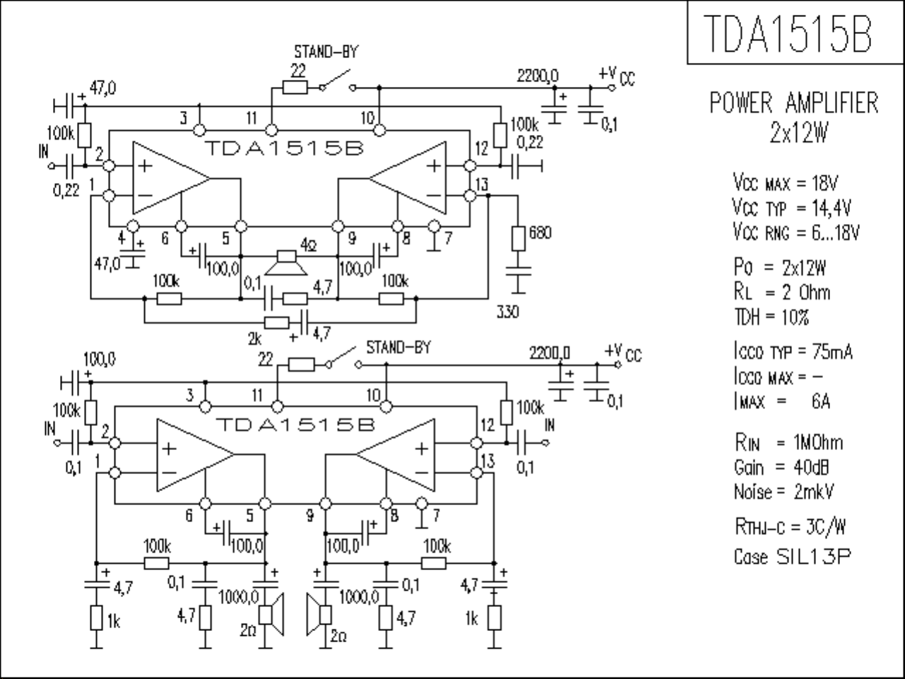
The TDA1515BQ is a monolithic integrated class-B output amplifier in a 13-lead single in-line (SIL) plastic power
package. The device is primarily developed for car radio applications, and also to drive low-impedance loads (down to
1,6 Ω). At a supply voltage VP= 14,4 V, an output power of 24 W can be delivered into a 4 Ω BTL (Bridge Tied Load),
or, when used as stereo amplifier, it delivers 2 × 12 W into 2 Ω or 2 × 7 W into 4 Ω.
Special features are:
• flexibility in use − mono BTL as well as stereo
• high output power
• low offset voltage at the output (important for BTL)
• large usable gain variation
• very good ripple rejection
• internal limited bandwidth for high frequencies
• low stand-by current possibility (typ. 1 µA), to simplify required switches; TTL drive possible
• low number and small sized external components
• high reliability.
The following currently required protections are incorporated in the circuit. These protections also have positive influence
on reliability in the applications.
• load dump protection
• a.c. and d.c. short-circuit safe to ground up to VP= 18 V
• thermal protection
• speaker protection in bridge configuration
• SOAR protection
• outputs short-circuit safe to ground in BTL
• reverse polarity safe.
July 1994 2
Page 3

Philips Semiconductors Product specification
24 W BTL or 2 x 12 W stereo
car radio power amplifier
QUICK REFERENCE DATA
Supply voltage range (operating) V
Supply voltage (non-operating) V
Supply voltage (non-operating; load dump protection) V
Repetitive peak output current I
Total quiescent current I
Stand-by current I
Switch-on current I
Input impedance |Z
Bridge tied load application (BTL) V
Output power at R
= 0,5% P
d
tot
= 10% P
d
tot
Supply voltage ripple rejection; R
D.C. output offset voltage between the outputs |∆V
= 4 Ω (with bootstrap)
L
= 0 Ω; f = 100 Hz RR typ. 50 50 dB
S
TDA1515BQ
P
P
P
ORM
tot
sb
so
|> 1MΩ
i
P
o
o
| < 50 50 mV
5-9
max. 28 V
max. 45 V
max. 4 A
typ. 75 mA
typ. 1 µA
< 100 µA
= 14,4 13,2 V
typ. 18 15 W
typ. 24 20 W
6 to 18 V
Stereo application
Output power at d
= 4 Ω P
R
L
= 2 Ω P
R
L
Output power at d
= 4 Ω P
R
L
R
= 2 Ω P
L
= 10% (with bootstrap)
tot
= 0,5% (with bootstrap)
tot
o
o
o
o
typ. 7 6 W
typ. 12 10 W
typ. 5,5 4,5 W
typ. 9 7,5 W
Channel separation α >40 40dB
Noise output voltage; R
= 10 kΩ; according to IEC curve-A V
S
n
typ. 0,2 0,2 mV
PACKAGE OUTLINE
13-lead SIL-bent-to-DIL; plastic power (SOT141C); SOT141-6; 1996 July 19.
July 1994 3
Page 4
Philips Semiconductors Product specification
24 W BTL or 2 x 12 W stereo
car radio power amplifier
TDA1515BQ
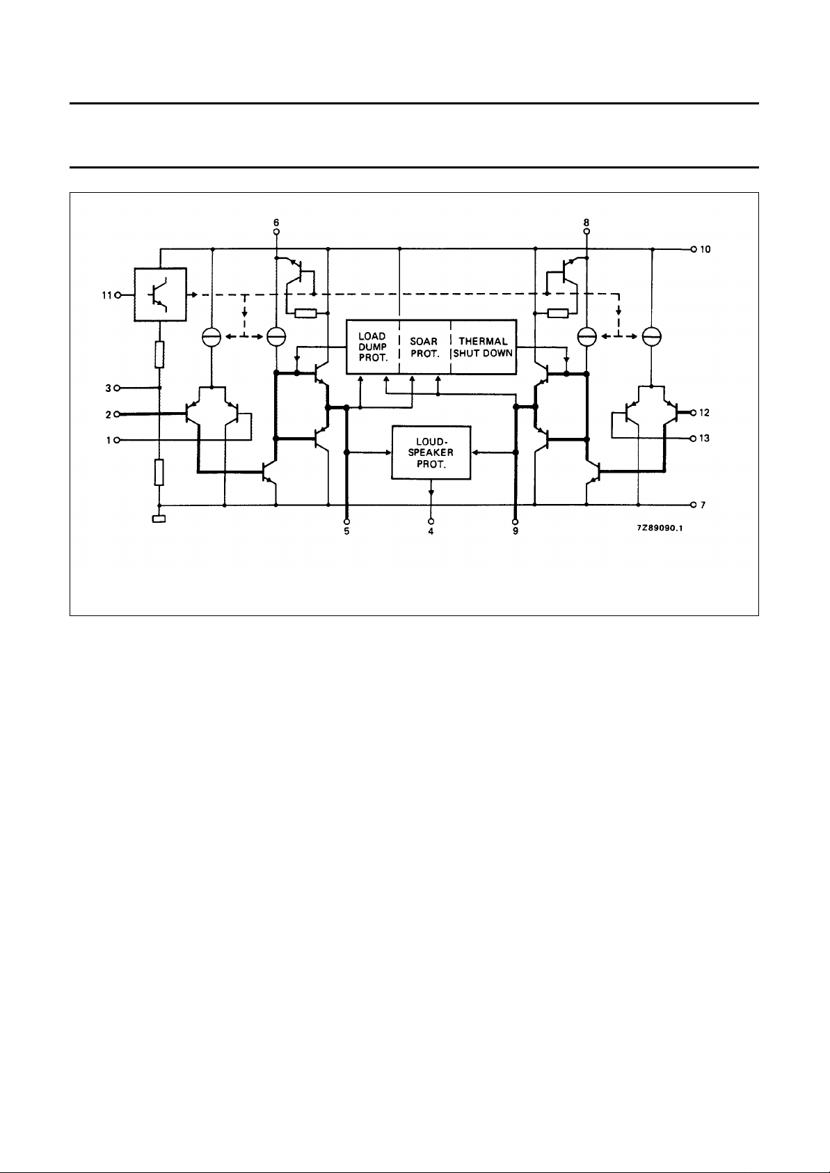
Fig.1 Internal block diagram; the heavy lines indicate the signal paths.
RATINGS
Limiting values in accordance with the Absolute Maximum System (IEC 134)
Supply voltage; operating (pin 10) V
Supply voltage; non-operating V
Supply voltage; during 50 ms (load dump protection) V
Peak output current I
Total power dissipation see derating curve Fig.2
Storage temperature range T
Crystal temperature T
A.C. and d.c. short-circuit safe voltage max. 18 V
Reverse polarity max. 10 V
P
P
P
OM
stg
c
max. 18 V
max. 28 V
max. 45 V
max. 6 A
−55 to + 150 °C
max. 150 °C
July 1994 4
Page 5
Philips Semiconductors Product specification
24 W BTL or 2 x 12 W stereo
car radio power amplifier
TDA1515BQ
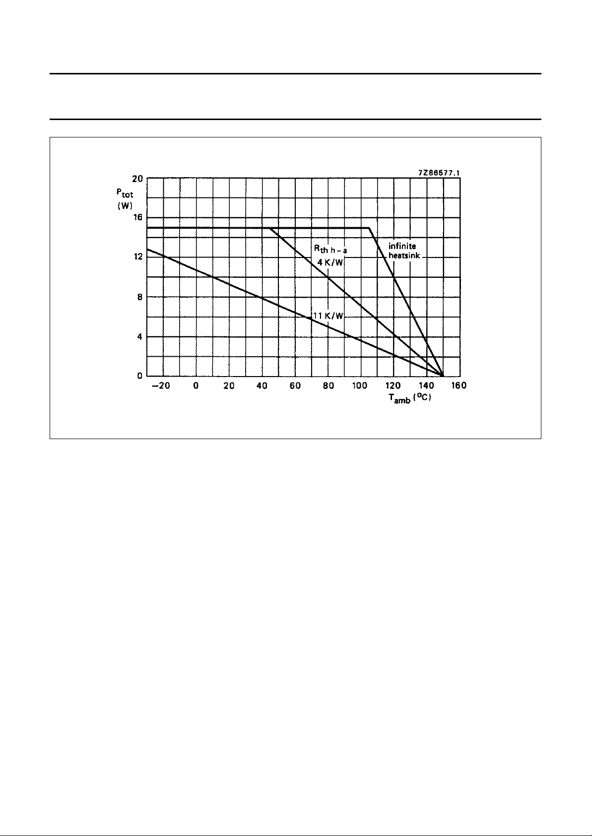
Fig.2 Power derating curves.
HEATSINK DESIGN EXAMPLE
The derating of 3 K/W of the encapsulation requires the following external heatsink (for sine-wave drive):
24 W BTL (4 Ω) or 2 × 12 W stereo (2 Ω)
maximum sine-wave dissipation: 12 W
T
= 65 °C maximum
amb
R
th h-a
2 × 7 W stereo (4 Ω)
maximum sine-wave dissipation: 6 W
T
amb
R
th h-a
150 65–
---------------------12
= 65 °C maximum
150 65–
----------------------
6
3– 4 K/W===
3– 11 K/W===
July 1994 5
Page 6

Philips Semiconductors Product specification
24 W BTL or 2 x 12 W stereo
TDA1515BQ
car radio power amplifier
D.C. CHARACTERISTICS
Supply voltage range (pin 10) V
Repetitive peak output current I
Total quiescent current I
Switching level 11: OFF V
ON V
Impedance between pins 10 and 6; 10 and 8 (stand-by position V
Stand-by current at V
Switch-on current (pin 11) at V
= 0 to 0,8 V I
11
≤ V10 (note 1) I
11
< 1,8 V) |Z
11
P
ORM
tot
11
11
OFF
<4A
typ. 75 mA
< 1,8 V
>3V
| > 100 kΩ
typ. 1 µA
sb
< 100 µA
typ. 10 µA
so
< 100 µA
A.C. CHARACTERISTICS
T
= 25 °C; VP= 14,4 V; f = 1 kHz; unless otherwise specified
amb
Bridge tied load application (BTL); see Fig.3
Output power at R
= 14,4 V; d
V
P
= 14,4 V; d
V
P
= 13,2 V; d
V
P
= 13,2 V; d
V
P
Open loop voltage gain G
Closed loop voltage gain (note 2) G
= 4 Ω (with bootstrap)
L
= 0,5% P
tot
= 10% P
tot
= 0,5% P
tot
= 10% P
tot
o
typ. 18 W
>20W
> 15,5 W
o
o
o
o
c
typ. 24 W
typ. 15 W
typ. 20 W
typ. 75 dB
typ. 40 (± 0,5) dB
Output power without bootstrap (note 9)
= 14,4 V; d
V
P
= 14,4 V; d
V
P
= 13,2 V; d
V
P
= 13,2 V; d
V
P
= 10% P
tot
= 0,5% P
tot
= 10% P
tot
= 0,5% P
tot
o
o
o
o
typ. 15 W
typ. 12 W
typ. 12 W
typ. 9 W
Frequency response at −3 dB (note 3) B 20 Hz to min. 20 kHz
Input impedance (note 4) |Zi|> 1MΩ
Noise input voltage (r.m.s. value) at f = 20 Hz to 20 kHz
= 0 Ω V
R
S
= 10 kΩ V
R
S
= 10 kΩ; according to IEC 179 curve A V
R
S
n(rms)
n(rms)
n
typ. 0,2 mV
typ. 0,35 mV
< 0,8 mV
typ. 0,25 mV
Supply voltage ripple rejection (note 5)
f = 100 Hz RR
>42dB
typ. 50 dB
6 to 18 V
July 1994 6
Page 7

Philips Semiconductors Product specification
24 W BTL or 2 x 12 W stereo
TDA1515BQ
car radio power amplifier
D.C. output offset voltage between the outputs |∆V
5-9
|
Loudspeaker protection (all conditions)
maximum d.c. voltage (across the load) |∆V
Power bandwidth; −1 dB; d
= 0,5% B 30 Hz to 40 kHz
tot
|< 1V
5-9
Stereo application; see Fig.4
Output power at d
= 14,4 V; RL = 4 Ω P
V
P
= 14,4 V; RL = 2 Ω P
V
P
= 13,2 V; RL = 4 Ω P
V
P
= 13,2 V; RL = 2 Ω P
V
P
Output power at d
= 14,4 V; RL = 4 Ω P
V
P
= 14,4 V; RL = 2 Ω P
V
P
= 13,2 V; RL = 4 Ω P
V
P
= 13,2 V; RL = 2 Ω P
V
P
Output power at d
= 14,4 V; RL = 4 Ω (notes 6, 8 and 9) P
V
P
= 10%; with bootstrap (note 6)
tot
= 0,5%; with bootstrap (note 6)
tot
= 10%; without bootstrap
tot
o
o
o
o
o
o
o
o
o
Frequency response at −3 dB (note 3) B 40 Hz to min. 20 kHz
Supply voltage ripple rejection (note 5) RR typ. 50 dB
Channel separation; R
Closed loop voltage gain (note 7) G
= 10 kΩ; f = 1 kHz α
S
c
Noise output voltage (r.m.s. value) at f = 20 Hz to 20 kHz
= 0 Ω V
R
S
= 10 kΩ V
R
S
= 10 kΩ; according to IEC 179 curve A V
R
S
n(rms)
n(rms)
n
Notes
1. The internal circuit impedance at pin 11 is > 5 kΩ if V11 > V10.
2. Closed loop voltage gain can be chosen between 32 and 56 dB (BTL), and is determined by external components.
For further gain reduction see Application Report.
3. Frequency response externally fixed.
4. The input impedance in the test circuit (Fig.3) is typ. 100 kΩ.
5. Supply voltage ripple rejection measured with a source impedance of 0 Ω (maximum ripple amplitude: 2 V).
6. Output power is measured directly at the output pins of the IC.
7. Closed loop voltage gain can be chosen between 26 and 50 dB (stereo), and is determined by external components.
8. A resistor of 56 kΩ between pins 3 and 7 to reach symmetrical clipping.
9. Without bootstrap the 100 µF capacitor between pins 5 and 6 (8 and 9) can be omitted. Pins 6, 8 and 10 have to be
interconnected.
<50mV
typ. 2 mV
>6W
typ. 7 W
>10W
typ. 12 W
typ. 6 W
typ. 10 W
typ. 5,5 W
typ. 9 W
typ. 4,5 W
typ. 7,5 W
typ. 6 W
>40dB
typ. 50 dB
typ. 40 dB
typ. 0,15 mV
typ. 0,25 mV
typ. 0,2 mV
July 1994 7
Page 8
Philips Semiconductors Product specification
24 W BTL or 2 x 12 W stereo
car radio power amplifier
TDA1515BQ
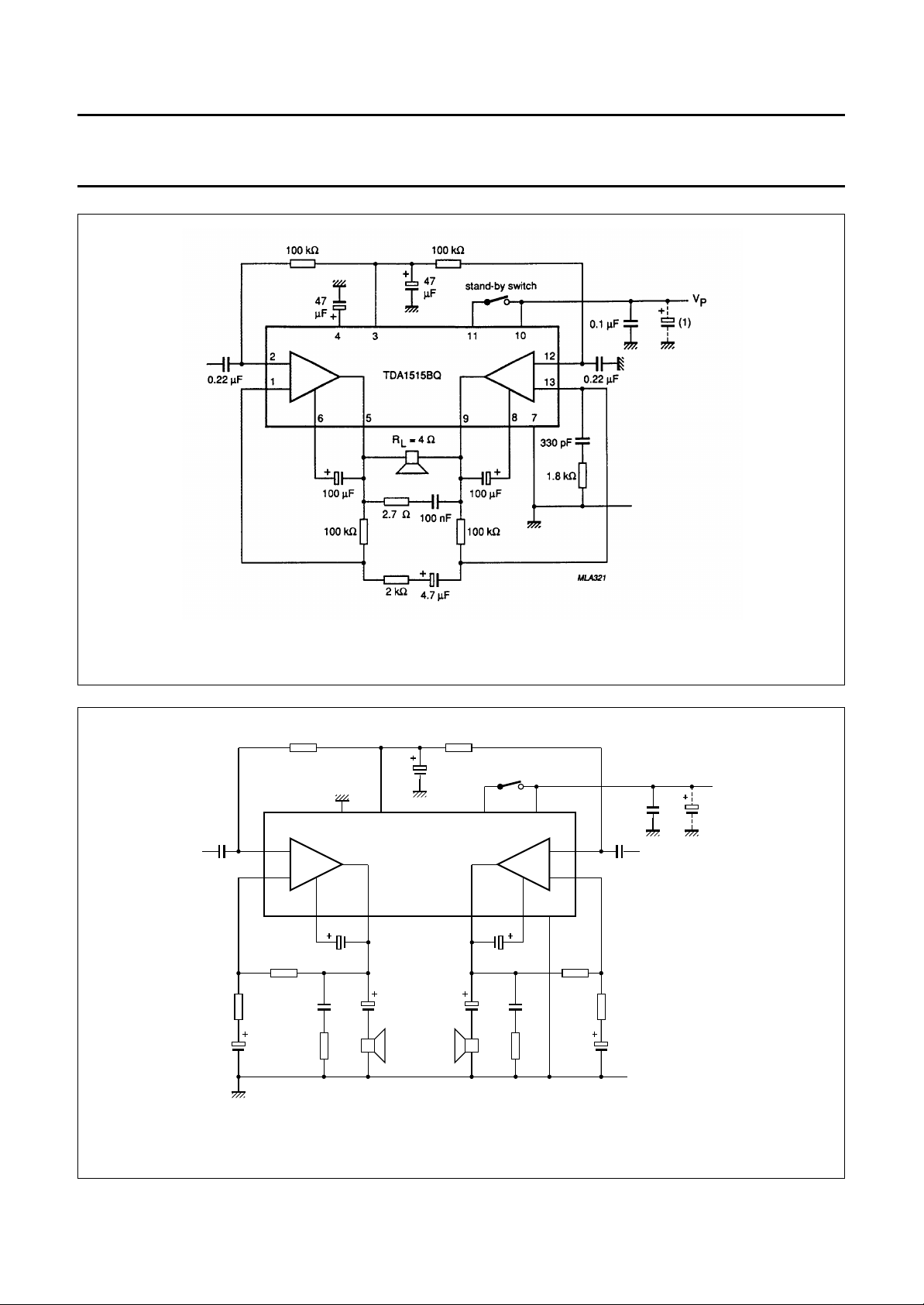
(1) Belongs to power supply.
handbook, full pagewidth
Fig.3 Test/application circuit bridge tied load (BTL).
100 kΩ 100 kΩ
47
stand-by switch
µF
4 3 11 10
2
0.1 µF 0.1 µF
1
65 987
100 kΩ 100 kΩ
1 kΩ 0.1 µF
4.7 Ω10 µF
TDA1515BQ
1 mF 1 mF
R
R
L
L
100 µF100 µF
0.1
µF
4.7
Ω
12
13
10 µF
0.1 µF
1 kΩ
(1)
V
P
(1) Belongs to power supply.
Fig.4 Test/application circuit stereo.
July 1994 8
MLA320 - 1
Page 9
Philips Semiconductors Product specification
24 W BTL or 2 x 12 W stereo
car radio power amplifier
PACKAGE OUTLINE
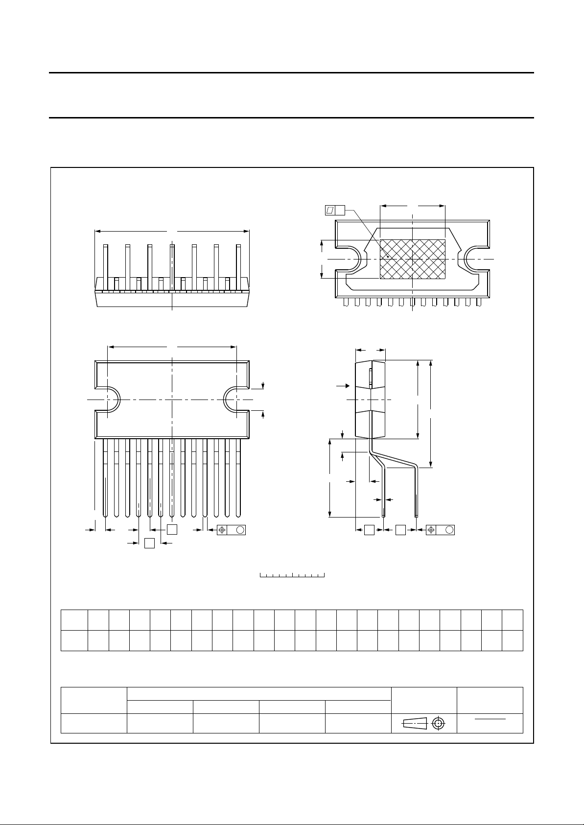
DBS13P: plastic DIL-bent-SIL power package; 13 leads (lead length 12 mm)
non-concave
x
D
E
h
d
A
TDA1515BQ
D
h
view B: mounting base side
2
SOT141-6
j
113
e
Z
DIMENSIONS (mm are the original dimensions)
UNIT A e
mm
Note
1. Plastic or metal protrusions of 0.25 mm maximum per side are not included.
A2bpcD
17.0
4.6
4.2
0.75
0.60
15.5
1
e
(1)
deD
0.48
24.0
23.6
20.0
19.6
0.38
b
p
h
10 3.4
w M
0 5 10 mm
scale
(1)
E
12.2
11.8
1
1.7
e
5.08
B
E
A
L
3
L
E
2
h
6
Q
c
m
LL3m
3.4
12.4
3.1
11.0
2.4
1.6
e
2
4.3
2.1
1.8
v M
(1)
v
Qj
0.8
0.25w0.03
Z
x
2.00
1.45
OUTLINE
VERSION
SOT141-6
IEC JEDEC EIAJ
REFERENCES
July 1994 9
EUROPEAN
PROJECTION
ISSUE DATE
92-11-17
95-03-11
Page 10

Philips Semiconductors Product specification
24 W BTL or 2 x 12 W stereo
car radio power amplifier
SOLDERING
Introduction
There is no soldering method that is ideal for all IC
packages. Wave soldering is often preferred when
through-hole and surface mounted components are mixed
on one printed-circuit board. However, wave soldering is
not always suitable for surface mounted ICs, or for
printed-circuits with high population densities. In these
situations reflow soldering is often used.
This text gives a very brief insight to a complex technology.
A more in-depth account of soldering ICs can be found in
“IC Package Databook”
our
Soldering by dipping or by wave
The maximum permissible temperature of the solder is
260 °C; solder at this temperature must not be in contact
with the joint for more than 5 seconds. The total contact
time of successive solder waves must not exceed
5 seconds.
(order code 9398 652 90011).
TDA1515BQ
The device may be mounted up to the seating plane, but
the temperature of the plastic body must not exceed the
specified maximum storage temperature (T
printed-circuit board has been pre-heated, forced cooling
may be necessary immediately after soldering to keep the
temperature within the permissible limit.
Repairing soldered joints
Apply a low voltage soldering iron (less than 24 V) to the
lead(s) of the package, below the seating plane or not
more than 2 mm above it. If the temperature of the
soldering iron bit is less than 300 °C it may remain in
contact for up to 10 seconds. If the bit temperature is
between 300 and 400 °C, contact may be up to 5 seconds.
stg max
). If the
DEFINITIONS
Data sheet status
Objective specification This data sheet contains target or goal specifications for product development.
Preliminary specification This data sheet contains preliminary data; supplementary data may be published later.
Product specification This data sheet contains final product specifications.
Limiting values
Limiting values given are in accordance with the Absolute Maximum Rating System (IEC 134). Stress above one or
more of the limiting values may cause permanent damage to the device. These are stress ratings only and operation
of the device at these or at any other conditions above those given in the Characteristics sections of the specification
is not implied. Exposure to limiting values for extended periods may affect device reliability.
Application information
Where application information is given, it is advisory and does not form part of the specification.
LIFE SUPPORT APPLICATIONS
These products are not designed for use in life support appliances, devices, or systems where malfunction of these
products can reasonably be expected to result in personal injury. Philips customers using or selling these products for
use in such applications do so at their own risk and agree to fully indemnify Philips for any damages resulting from such
improper use or sale.
July 1994 10
Page 11
Page 12

 Loading...