

Page 1

Philips Semiconductors Product specification
Digital servo processor (DSIC2) TDA1301T
FEATURES
The DSIC2 realizes the following servo functions:
• Diode signal preprocessing
• Focus servo loop
• Radial servo loop
• Sledge motor servo loop
• Three-line serial interface via the microcontroller
The other features include:
• Full digital signal processing
• Low power consumption, down to 30 mW
• Low voltage supply 3 to 5.5 V
• Integrated analog-to-digital converters and digital servo
loop filters
• Double speed possible
• Easy application
– Single supply voltage
– Small number of external components; only
6 decoupling capacitors
– Flexible system oscillator circuitry
– Usable for single/double Foucault and astigmatic
focus
– Full automatic radial error signal initialization offset
control and level initialization for track position
indicator
– No external adjustments required; no component
ageing
– Wide range of adjustable servo characteristics
– Simple 3-line serial command interface
– 28-pin SO package
– Great flexibility towards different CD mechanisms
– Full and transparent application information
• High robustness/shock insensitivity
– Sophisticated track-loss (TL) detection mechanism
– Fast focus restart procedure
– Extended radial error signal
– Adjustable radial shock detector
– Defect drop-out detector
• Fully automatic jump procedure for radial servo
• Automatic focus start-up procedure and built-in FOK
(Focus OK)
• Fast radial jump or access procedure
• Self-operational servo-control without continuous
communication via the microcontroller
• Direct communication to photodiode optics; no external
preprocessing.
GENERAL DESCRIPTION
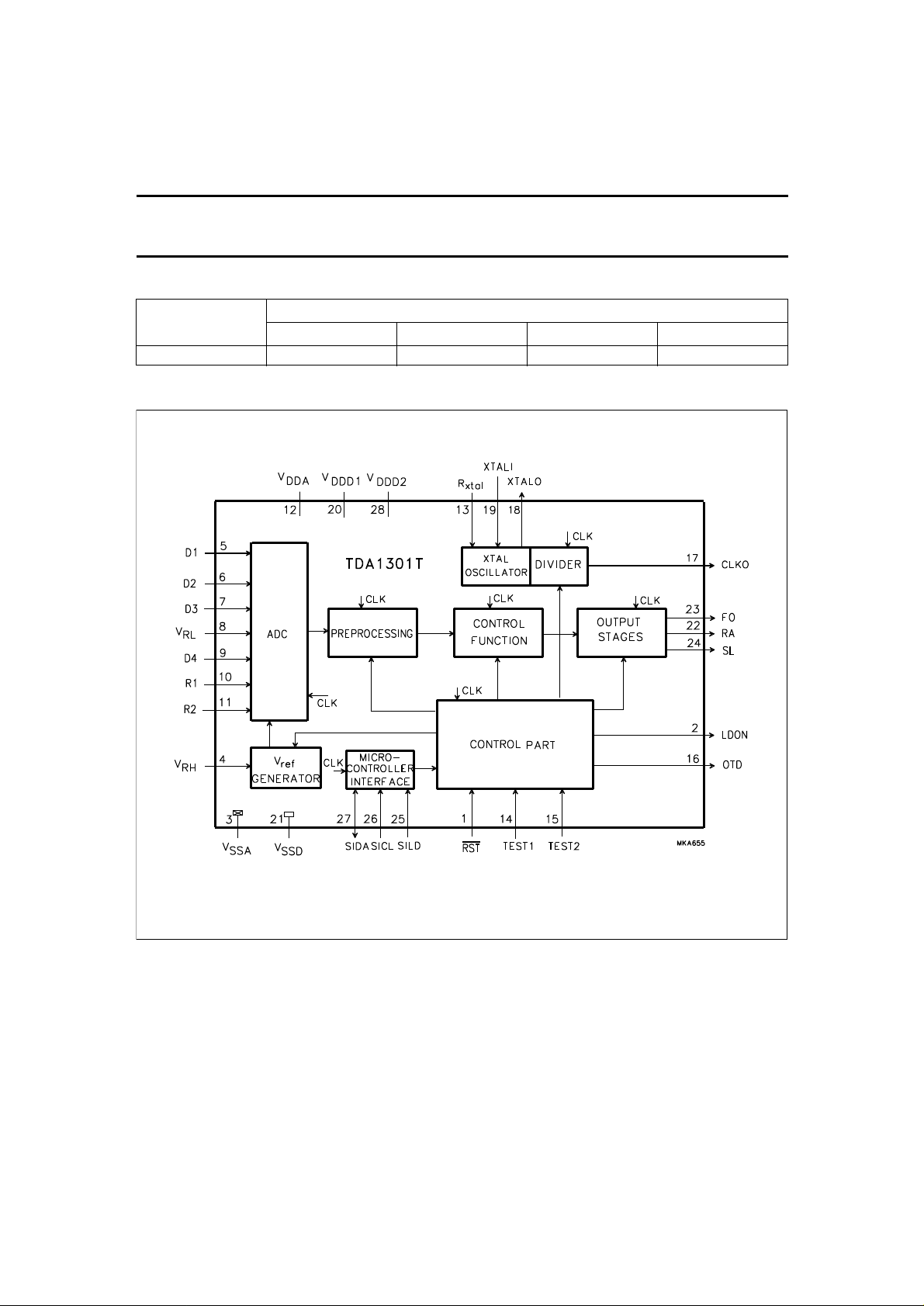
The TDA1301T is a fully digital servo processor which has
been designed to provide all servo functions, except the
spindle motor control, in two-stage three-spot compact
disc systems. The device offers a high degree of
integration, combined with the low additional cost of
external components. The servo characteristics have a
wide range of adjustment via a three-line serial interface.
This offers an enormous flexibility with respect to
applications for different CD mechanisms. The circuit is
optimized for low-power low-voltage applications.
QUICK REFERENCE DATA
SYMBOL PARAMETER CONDITIONS MIN. TYP. MAX. UNIT
V
DDD
V
DDA
I
DDD
I
DDA
I
DDD(q)
I
i(cd)
I
i(sd)
P
tot
T
amb
digital supply voltage 3.0 − 5.5 V
analog supply voltage 3.0 − 5.5 V
digital supply current − 5 − mA
analog supply current − 5 − mA
digital quiescent supply current − − 10 µA
central diode input currents (D1 to D4) note 1 − − 15.8 µA
satellite diode input currents (R1 and R2) note 1 − − 7.9 µA
total power dissipation − 50 − mW
operating ambient temperature −40 − +85 °C
Note
1. f
= 4.2336 MHz; VRL = 0 V; VRH = 2.5 V (externally applied).
sys
March 1994 2
Page 2
Philips Semiconductors Product specification
Fig.1 Block diagram.
Digital servo processor (DSIC2) TDA1301T
ORDERING INFORMATION
EXTENDED TYPE
NUMBER
TDA1301T 28 SO28L plastic SOT136A
BLOCK DIAGRAM
PINS PIN POSITION MATERIAL CODE
PACKAGE
March 1994 3
Page 3

Philips Semiconductors Product specification
Fig.2 Pin configuration.
Digital servo processor (DSIC2) TDA1301T
PINNING
SYMBOL PIN DESCRIPTION
RST 1 reset input (active LOW)
LDON 2 laser drive on output
V
SSA
V
RH
D1 5 unipolar current input
D2 6 unipolar current input
D3 7 unipolar current input
V
RL
D4 9 unipolar current input
R1 10 unipolar current input
R2 11 unipolar current input
V
DDA
XTAL
TEST1 14 test input 1
TEST2 15 test input 2
OTD 16 off-track detector output
CLKO 17 clock output
XTALO 18 oscillator output
XTALI 19 oscillator input
V
DDD1
V
SSD
RA 22 radial actuator output
FO 23 focus actuator output
SL 24 sledge output
SILD 25 serial interface load input
SICL 26 serial interface clock input
SIDA 27 serial interface data input/output
V
DDD2
3 analog ground
4 reference input for reference voltage
generator
(central diode signal input)
(central diode signal input)
(central diode signal input)
8 reference input for ADC
(central diode signal input)
(satellite diode signal input)
(satellite diode signal input)
12 analog supply voltage
13 oscillator reference input
ref
20 digital power supply 1
21 digital ground
28 digital power supply 2
March 1994 4
Page 4
Philips Semiconductors Product specification
–
]
]
4–
D3 D4+
----------------------
–=
Fig.3 Diode configuration.
Digital servo processor (DSIC2) TDA1301T
FUNCTIONAL DESCRIPTION
Three spots front-end
The photo detector in a two-stage three-spots compact
disc system normally contains six discrete elements. Four
of these elements (in the event of single Foucault: three
elements) carry the central aperture (CA) signal while the
other two elements (satellite signals) carry the radial
tracking information. Besides the HF signal, which is finally
applied to both of the audio channels, the central aperture
also contains information for the focus servo loop. To
enable the HF signal to be processed, the frequency
contents of the central aperture signal must be divided into
an HF data part and an LF servo part. The HF signal is
processed outside the DSIC2 by the TDA1302 or a
discrete amplifier-equalizer. The necessary crossover
point, to extract the LF servo part, is compensated for in
the amplifier.
Diode signal processing
The analog signals from the photo detectors are converted
into a digital representation using analog-to-digital
converters. The ADCs are designed to convert unipolar
currents into a digital code. The dynamic range of the input
currents is adjustable within a given range and is
dependent on the ADC input reference voltages V
and
RL
VRH. The maximum current for the central diodes signals
is given in equation (1).
I
i max( )fsysVRHVRL
( ) 1.5 106–×××= µA[
(1)
The maximum current for the satellite signals is given in
equation (2).
I
i max( )fsysVRHVRL
V
is generated internally. There are four different levels
RH
–( ) 0.75 106–×××= µA[
(2)
(1.0, 1.5, 2.0 and 2.5 V) which can be selected under
software control. In the application VRL is connected to
V
. It is also possible to drive VRH with an external
SSA
voltage source but in this situation the internal voltage
source has to be switched off (software controlled).
Signal conditioning
The digital codes retrieved from the ADCs are applied to
logic circuitry to obtain the various control signals. The
signals from the central aperture detectors are processed
so that the normalized focus error signal (FE) given in
equation (3) is realized:
FE
n
D1 D2–
---------------------D1 D2+
D3 D
(3)
Where the detector set-up is assumed to be as illustrated
in Fig.3.
March 1994 5
Page 5

Philips Semiconductors Product specification
( )
R1 R2+( ) Sum_gain×–
[]sin=
Digital servo processor (DSIC2) TDA1301T
In the event of single Foucault focusing method, the DSIC2
signal conditioning can be switched under software control
so that the signal processing conforms to that given in
equation (4).
FEn2
×=
---------------------D1 D2+
(4)
D1 D2–
The FEn thus obtained is further processed by a
proportional integral and differential filter section (PID).
A focus OK flag (FOK) is generated by means of the
central aperture signal and an adjustable reference level.
This signal is used to provide extra protection for the
Track-Loss (TL) generation, the focus start-up procedure
and the drop-out detection. The radial or tracking error
signal is generated by the satellite detector signals R1 and
R2. The radial error signal (RE) can be formulated as per
equation (5).
RE
=
s
R1 R2–( ) RE_gain×
R1 R2+( ) RE_offset×
+
(5)
Where the index ‘s’ indicates the automatic scaling
operation which is performed on the radial error signal.
This scaling is necessary to avoid non-optimum dynamic
range usage in the digital representation and, also, to
reduce radial bandwidth spread. The radial error signal will
also be released from offset during disc start-up. The four
signals from the central aperture detectors, together with
the satellite detector signals, generate a track position
signal (TPI) which can be formulated as per equation (6).
TPI D1 D2 D3 D4+ + +
(6)
Where the weighting factor Sum_gain is generated
internally in the DSIC2 during initialization.
Focus control
The following focus servo functions are incorporated in the
DSIC2 digital controller.
OCUS START-UP
F
Five initially loaded coefficients influence the start-up
behaviour of the focus controller. The automatically
generated triangular voltage can be influenced by
3 parameters, for the height (ramp_heigth) and DC-offset
(ramp_offset) of the triangle and its steepness (ramp_inc).
To protect against false focus point detections two
parameters are available. One is an absolute level on the
CA signal (CA_start) and the other is an absolute level on
the FEn signal (FE_start). When the CA_start level is
reached, the FOK signal becomes true. If the FOK signal
is true when the level on the FEn signal is reached the
focus PID is enabled and switches on when the next zero
crossing is detected in the FEn signal.
FOCUS POSITION CONTROL LOOP
The focus control loop contains a digital PID controller
which has 5 parameters available to the user. These
coefficients influence the integrating (foc_int), proportional
(foc_prop) and differentiating (foc_pole_lead) action of this
PID and the digital low-pass filter (foc_pole_noise) which
follows the PID. The fifth coefficient (foc_gain) influences
the loop gain.
D
ROP-OUT DETECTION
This detector can be influenced by one parameter
(CA_drop). The FOK signal will become false and the
integrator of the PID will hold if the CA signal drops below
the programmed absolute CA level. When the FOK signal
becomes false it is assumed, initially, to be caused by a
black dot.
FOCUS LOSS DETECTION AND FAST RESTART
Whenever FOK is false for longer than approximately
3 ms, it is assumed that the focus point is lost. A fast
restart procedure is initiated which is capable of restarting
the focus loop within 200 to 300 ms depending on the
programmed coefficients set by the microcontroller.
FOCUS LOOP GAIN SWITCHING
The gain of the focus control loop (foc_gain) can be
multiplied by a factor of 2 or divided by a factor of 2 during
normal operation. The integrator value of the PID is
corrected accordingly. The differentiating (foc_pole_lead)
action of the PID can be switched at the same time as the
gain switching is performed.
Radial control
The following radial servo functions are incorporated in
the DSIC2 digital controller.
LEVEL INITIALIZATION
During start-up an automatic adjustment procedure is
activated to set the values of the radial error gain
(RE_gain), offset (RE_offset) and satellite sum signal gain
(Sum_gain) for TPI level generation. The initialization
procedure runs in a radial open-loop situation and is
≤300 ms. This start-up time period may coincide with the
last part of the turn table motor start-up time period.
March 1994 6
Page 6

Philips Semiconductors Product specification
Digital servo processor (DSIC2) TDA1301T
Automatic gain adjustment: as a result of this initialization
the amplitude of the RE signal is adjusted within 10%
around the nominal RE amplitude.
Offset adjustment: the additional offset in RE due to
the limited accuracy of the start-up procedure is less
than 50 nm.
TPI level generation: the accuracy of the initialization
procedure is such that the duty cycle range of TPI
becomes 0.4 < δ < 0.6 {δ = TPI(HIGH)/TPI(period)}.
SLEDGE HOME
Sledge moves to reference position (end_stop_switch) at
the inner side of the disc with user defined voltage.
T
RACKING CONTROL
The actuator is controlled using a PID loop-filter with user
defined coefficients and gain. For stable operation
between the tracks, the S-curve is extended over3⁄4 track.
Upon request from the microcontroller S-curve extension
over 2 tracks is used, automatically changing to access
control when these two tracks are exceeded.
Both modes of S-curve extension make use of a
track-count mechanism as described in Section “Off-track
counting” . In this mode track counting results in automatic
‘return-to-zero track’, to avoid major music rhythm
disturbances in the audio output to provide improved
shock resistance. The sledge is continuously controlled
using the filtered value of the integrator contents of the
actuator, or upon request by the microcontroller. The
microcontroller can read out this integrator value and
provides the sledge with step pulses to reduce power
consumption. Filter coefficients of the continuous sledge
control can be preset by the user.
ACCESS
The access procedure is divided into 2 different modes,
depending on the requested jump size.
The access procedure makes use of a track counting
mechanism (see Section “Off-track counting” ), a velocity
signal based upon the number of tracks passed within a
fixed time interval, a velocity setpoint calculated from the
number of tracks to go and a user programmable
parameter indicating the maximum sledge performance.
If the number of tracks to go is greater than break_dist the
sledge jump mode will be activated (otherwise the actuator
jump will be performed). The requested jump size together
with the required sledge braking distance at maximum
access speed defines the value break_dist.
During the actuator jump mode, velocity control with a PI
controller is used for the actuator.
The sledge is then continuously controlled using the
filtered value of the integrator contents of the actuator.
All filter parameters (for actuator and sledge) are user
programmable.
In the sledge jump mode, maximum power (user
programmable) is applied to the sledge in the correct
direction, while the actuator becomes Idle (the contents of
the actuator integrator leaks to zero just after the sledge
jump mode is initiated).
Table 1 Access procedure.
ACCESS
TYPE
Actuator
JUMP SIZE ACCESS SPEED
1 − break distance
(1)
decreasing velocity
jump
Sledge
jump
break
(1)
− 32768 minimum power to
sledge
(1)
Note
1. Can be preset by the microcontroller.
Defect detector
A built-in defect detector prevents the light spot from going
out-of-focus and going off-track due to disc drop-out
excitations. The defect detector can be switched ON or
OFF under software control and can be applied to the
focus control only, or to both the focus and radial control.
The detected defect signal holds the focus and radial loop
filter outputs. The hold signal is generated whenever the
reflected light intensity drops rapidly (<1.5 ms) down to
75% of the actual intensity level.
Shock detector
The shock detector can be switched ON during normal
track following. The shock detector detects, within an
adjustable frequency band, whether the disturbances in
the radial spot position relative to the track exceeds an
adjustable level. Every time the radial tracking error (RE)
exceeds this level the radial control bandwidth is switched
directly to twice the original bandwidth.
The shock detection level is adjustable in 64 steps from
0 to 100% of the nominal radial amplitude. The bandpass
filter (BPF) lower frequency (−3 dB) can be fixed at 0 or
20 Hz. Independently, the BPF upper frequency (−3 dB)
can be fixed at 750 or 1850 Hz.
Off-track counting
TPI is a flag which is used to indicate whether the spot is
positioned on the track (with a margin of 1⁄4 of the
track-pitch).
March 1994 7
Page 7

Philips Semiconductors Product specification
Digital servo processor (DSIC2) TDA1301T
In combination with the radial polarity flag (RP) the relative
spot-position over the tracks can be determined. These
signals are, however, affected with some uncertainties
caused by:
• Disc defects such as scratches and fingerprints.
• The HF information on the disc, which is considered as
noise by the detector signals.
In order to determine the spot position with sufficient
accuracy, extra conditions are necessary to generate a TL
signal as well as an off-track counter value. These extra
conditions influence the maximum speed and this implies
that, internally, one of the three following counting states is
selected. These states are:
1. Protected state: used in normal play situations.
A good detection caused by disc defects is important
in this state.
2. Slow counting state: used in low velocity track jump
situations.
In this state a fast response is important rather than
the protection against disc defects (if the phase
relationship between TL and RP of a1⁄2π rad is affected
too much, the direction cannot be determined
accurately any more).
3. Fast counting state: used in high velocity track jump
situations.
Highest obtainable velocity is the most important
feature in this state.
Off-track detection
During active radial tracking, off-track detection is realized
by continuously monitoring the off-track counter value. The
off-track flag (OTD) becomes valid whenever the off-track
counter value is not equal to zero. Depending on the type
of extended S-curve the off-track counter will be reset after
3
⁄4 extend or at the original track in the 21⁄4 track extend
mode.
Output stages
The control signals for the different actuators are 1-bit
noise shaped digital outputs at 1.0584 MHz. An analog
representation of the output signals can be achieved by
connecting a first-order low-pass filter to the outputs.
When the
sledge output stages are 3-state.
Serial interface
To control the DSIC2 operation, a serial interface is
implemented which allows communication with a
microcontroller via a 3-line serial bus consisting of:
RST pin is held LOW, the focus, radial and
• Serial clock line (SICL
• Serial data line (SIDA)
• Serial control line (SILD).
The SICL line is controlled by a microcontroller and can be
completely asynchronous from the oscillator frequency of
the DSIC2. The SILD line is used for read/write control and
end-of-byte signalling.
The communication is bi-directional and processes 8-bit
words (1 byte, MSB first). The data present on the SIDA
line is clocked on the positive edge of SICL. One
information exchange consists of one command byte and
up to 7 data bytes.
The first byte defines the command, and is always input to
the DSIC2. This byte defines if data has to be written to or
read from the DSIC2. If data has to be written to the DSIC2
this byte also specifies the number of data bytes. The
number of bytes read from the DSIC2 can vary from 0 up
to 5 and only depends on how many the microprocessor
requires to read. Further information concerning the serial
protocol is available upon request.
Clock generation
The DSIC2 operates with an internal clock frequency of
approximately 4 MHz. The circuit that generates the clock
has three modes: the oscillator frequency divided by 2, 3
or 4 (software controlled). It is therefore possible to
connect a crystal or a resonator with a frequency of
8.4672, 11.2896 or 16.9344 MHz. These frequencies are
derived from today’s frequently used decoder IC
frequencies. It is also possible to drive the clock circuit with
an external clock signal. The clock buffer output (CLKO)
can supply the system clock or twice the system clock
(also switchable under software control via the serial bus)
to be used as a clock generator for other ICs. The oscillator
circuit is optimized for low power dissipation. To guarantee
optimum performance with a quartz crystal or a resonator
the gain of the oscillator can be adjusted by an external
resistor connected to the XTAL
Reset
The reset is controlled by means of the
LOW). This circuit ensures proper initialization of the
digital circuit and the output stages.
Laser drive on
The LDON pin is used to switch the laser drive OFF and
ON. It is an open-drain output. When the laser is ON, the
output has a high impedance.
ref
input.
RST pin (active
March 1994 8
Page 8

Philips Semiconductors Product specification
Digital servo processor (DSIC2) TDA1301T
LIMITING VALUES
In accordance with the Absolute Maximum Rating System (IEC 134).
SYMBOL PARAMETER MIN. MAX. UNIT
V
DDD
V
DDA
∆V
SS
P
max
T
stg
T
amb
HANDLING
Classification A: human body model; C = 100 pF; R = 1500 Ω; V ≥ 2000 V.
Charge device model: C = 200 pF; R = 0 Ω; V ≥ 250 V.
Pulse widths in accordance with
pocket-book”
THERMAL RESISTANCE
SYMBOL PARAMETER THERMAL RESISTANCE
R
th j-a
digital supply voltage 0 6.5 V
analog supply voltage 0 6.5 V
difference in ground supply voltage between V
SSA
and V
−5.0 +5.0 mV
SSD
maximum power dissipation − 100 mW
storage temperature −65 +150 °C
operating ambient temperature −40 +85 °C
“UZW-BO/FQ-A302 and B302”
are applicable and can be found in the
“Quality reference
(ordering number 9398 510 34011).
from junction to ambient in free air 80 K/W
March 1994 9
Page 9

Philips Semiconductors Product specification
Digital servo processor (DSIC2) TDA1301T
CHARACTERISTICS
V
= V
DDA
= 5 V; V
DDD
SYMBOL PARAMETER CONDITIONS MIN. TYP. MAX. UNIT
Supply
V
DDD
V
DDA
I
DDD
I
DDA
I
DDD(q)
P
tot
digital supply voltage 3.0 − 5.5 V
analog supply voltage 3.0 − 5.5 V
digital supply current − 5 − mA
analog supply current − 5 − mA
quiescent current − − 60 µA
total power dissipation −40 − +85 °C
Analog part
I
i(cd)max
maximum input current for
central diode input signal
I
i(sd)max
maximum input current for
satellite diode input signal
V
RH
HIGH level reference voltage note 2
output stage 1 0.9 1.0 1.1 V
output stage 2 1.35 1.5 1.65 V
output stage 3 1.8 2.0 2.2 V
output stage 4 2.25 2.5 2.75 V
PSRR power supply ripple rejection
at pin 4
V
RH
V
RL
HIGH level reference voltage input state; note 4 0.5 − V
LOW level reference voltage 0 V
(THD+N)/S total harmonic distortion plus
signal-to-noise ratio
S/N signal-to-noise ratio − 55 − dB
PSRR power supply ripple rejection
at pin 12
G
tol
gain tolerance note 6 −10 − +15 %
∆G variation of gain between
channels
α
cs
channel separation − 60 − dB
Digital part
I
NPUTS: TEST1, TEST2, SICL AND SILD
V
IL
V
IH
I
LI
LOW level input voltage T
HIGH level input voltage T
input leakage current − − 10 µA
INPUT: NRST
V
IL
V
IH
I
LI
LOW level input voltage T
HIGH level input voltage T
input leakage current − − 10 µA
SSA
= V
SSD
= 0 V; T
= 25 °C; unless otherwise specified.
amb
note 1 − 15.8 − µA
note 1 − 7.9 − µA
note 3 45 55 − dB
DDA
− 1.5 − V
DDA
at 0 dB; note 5 − −50 −45 dB
note 3 − 45 − dB
− − 2 %
= −40 to +85 °C − − 0.3V
amb
= −40 to +85 °C 0.75V
amb
= −40 to +85 °C − − 0.2V
amb
= −40 to +85 °C 0.8V
amb
− − V
DDD
− − V
DDD
− 0.5 V
DDD
DDD
V
V
March 1994 10
Page 10

Philips Semiconductors Product specification
Digital servo processor (DSIC2) TDA1301T
SYMBOL PARAMETER CONDITIONS MIN. TYP. MAX. UNIT
OUTPUTS: CLKO AND OTD
I
OL
I
OH
t
r
t
f
OUTPUT: LDON
I
OL
I
OZ
t
r
t
f
OUTPUTS; RA, FO AND SL
I
OL
I
OH
I
OZ
t
r
t
f
INPUT/OUTPUT: SIDA
V
IL
V
IH
I
OL
I
OH
I
OZ
t
r
t
f
OSCILLATOR
f
osc
C
i
C
o
C
fb
R
xtal
R
ext
V
19(p-p)
LOW level output current VOL = 0.4 V 1.6 − − mA
HIGH level output current VOH = V
− 0.4 V 1.3 − − mA
DDD
rise time note 7 − − 44 ns
fall time note 7 − − 40 ns
LOW level output current VOL = 0.4 V 3.3 − − mA
3-state output leakage current T
= −40 to +85 °C;
amb
VO = V
SSD/VDDD
− − 1.5 µA
rise time, LOW to 3-state CL = 50 pF − − 37 ns
fall time, 3-state to LOW CL = 50 pF − − 20 ns
LOW level output current VOL = 0.4 V 3.3 − − mA
HIGH level output current VOH = V
3-state output leakage current T
amb
VO = V
− 0.4 V 1.8 − − mA
DDD
= −40 to +85 °C;
SSD/VDDD
− − 1.5 µA
rise time note 7 − − 37 ns
fall time note 7 − − 20 ns
LOW level input voltage T
HIGH level input voltage T
= −40 to +85 °C − − 0.3V
amb
= −40 to +85 °C 0.75V
amb
− − V
DDD
DDD
V
LOW level output sink current VOL = 0.4 V 3.3 − − mA
HIGH level output source
VOH = V
− 0.4 V 1.8 − − mA
DDD
current
3-state output leakage current T
= −40 to +85 °C;
amb
VO = V
SSD
or V
− − 1.5 µA
DDD
rise time note 7 − − 37 ns
fall time note 7 − − 20 ns
oscillator frequency 8 − 17 MHz
input capacitance − − 4 pF
output capacitance − − 4 pF
feedback capacitance − − 3 pF
external oscillator reference
note 8 25 − 100 kΩ
resistor
external reference resistor note 9 − 10 − kΩ
minimum input clock voltage
level from external oscillator
(peak-to-peak value)
AC-coupled;
R
= 10 kΩ;
ext
R
= 1 MΩ connected
bias
− 500 − mV
between pins 18 and 19
March 1994 11
Page 11

Philips Semiconductors Product specification
Digital servo processor (DSIC2) TDA1301T
SYMBOL PARAMETER CONDITIONS MIN. TYP. MAX. UNIT
Slave clock mode: XTALI
V
IL
V
IH
t
H
Notes
1. f
sys
2. Internal reference source with 4 different output voltages. Selection is achieved via the serial interface. The given
values are for an unloaded reference voltage.
3. f
ripple
4. Internal reference is switched OFF by serial interface. VRH is the reference input.
5. Externally applied VRH = 2.5 V and VRL = 0 V, measuring bandwidth: 200 Hz to 20 kHz, f
6. The gain of the ADC is defined as: G
output is the number of pulses at the digital output in counts per second and II is the DC input current in mA.
The maximum input current depends on the system frequency (f
For D1 to D4: I
For R1 and R2: I
The gain tolerance is the deviation from the calculated gain regarding note 1.
7. At 10 to 90% levels with CL = 50 pF.
8. A resistor must be connected to set the gain of the oscillator circuit. The value of the resistor depends on the crystal
or resonator connected to the oscillator circuit (see also Chapter “Application information” ).
9. When the TDA1301T is supplied by an external oscillator frequency, no crystal or resonator is required while the
external reference resistor has different limits.
LOW level input voltage − − 0.5 V
HIGH level input voltage 2.0 − − V
HIGH level input time relative to the clock
45 − 55 %
period
= 4.2336 MHz; VRL = 0 V; VRH = 2.5 V (externally applied).
= 1 kHz; V
= 0.5 V (p-p).
ripple
= 1.5 × f
i(max)
i(max)
sys
= 0.75 × f
× V
sys
ref
× V
= f
ADC
sys/Imax
× 10−6/Ri× f
× 10−6/Ri× f
ref
i(ADC)
(counts/mA). Thus the digital output is II× G
sys
[µA].
sys
[µA].
) and on V
sys
= VRH− V
ref
RL
= 1 kHz.
where: digital
ADC
March 1994 12
Page 12

Philips Semiconductors Product specification
Fig.4 Application diagram.
(1)
1
⁄
2
V
DDD
= OFF.
Digital servo processor (DSIC2) TDA1301T
APPLICATION INFORMATION
March 1994 13
Page 13

Philips Semiconductors Product specification
Fig.5 28-lead small-outline; plastic (SO28L, SOT136A).
handbook, full pagewidth
7.6
7.4
10.65
10.00
A
MBC236 - 1
0.3
0.1
2.45
2.25
1.1
0.5
0.32
0.23
1.1
1.0
0 to 8
o
2.65
2.35
detail A
S
18.1
17.7
0.1 S
1 14
1528
pin 1
index
0.9
0.4
(4x)
0.25 M
(28x)
0.49
0.36
1.27
Dimensions in mm.
Digital servo processor (DSIC2) TDA1301T
PACKAGE OUTLINE
March 1994 14
Page 14

Philips Semiconductors Product specification
Digital servo processor (DSIC2) TDA1301T
SOLDERING
Plastic small-outline packages
B
Y WAVE
During placement and before soldering, the component
must be fixed with a droplet of adhesive. After curing the
adhesive, the component can be soldered. The adhesive
can be applied by screen printing, pin transfer or syringe
dispensing.
Maximum permissible solder temperature is 260 °C, and
maximum duration of package immersion in solder bath is
10 s, if allowed to cool to less than 150 °C within 6 s.
Typical dwell time is 4 s at 250 °C.
A modified wave soldering technique is recommended
using two solder waves (dual-wave), in which a turbulent
wave with high upward pressure is followed by a smooth
laminar wave. Using a mildly-activated flux eliminates the
need for removal of corrosive residues in most
applications.
BY SOLDER PASTE REFLOW
Reflow soldering requires the solder paste (a suspension
of fine solder particles, flux and binding agent) to be
applied to the substrate by screen printing, stencilling or
pressure-syringe dispensing before device placement.
DEFINITIONS
Several techniques exist for reflowing; for example,
thermal conduction by heated belt, infrared, and
vapour-phase reflow. Dwell times vary between 50 and
300 s according to method. Typical reflow temperatures
range from 215 to 250 °C.
Preheating is necessary to dry the paste and evaporate
the binding agent. Preheating duration: 45 min at 45 °C.
EPAIRING SOLDERED JOINTS (BY HAND-HELD SOLDERING
R
IRON OR PULSE
-HEATED SOLDER TOOL)
Fix the component by first soldering two, diagonally
opposite, end pins. Apply the heating tool to the flat part of
the pin only. Contact time must be limited to 10 s at up to
300 °C. When using proper tools, all other pins can be
soldered in one operation within 2 to 5 s at between
270 and 320 °C. (Pulse-heated soldering is not
recommended for SO packages.)
For pulse-heated solder tool (resistance) soldering of VSO
packages, solder is applied to the substrate by dipping or
by an extra thick tin/lead plating before package
placement.
Data sheet status
Objective specification This data sheet contains target or goal specifications for product development.
Preliminary specification This data sheet contains preliminary data; supplementary data may be published later.
Product specification This data sheet contains final product specifications.
Limiting values
Limiting values given are in accordance with the Absolute Maximum Rating System (IEC 134). Stress above one or
more of the limiting values may cause permanent damage to the device. These are stress ratings only and operation
of the device at these or at any other conditions above those given in the Characteristics sections of the specification
is not implied. Exposure to limiting values for extended periods may affect device reliability.
Application information
Where application information is given, it is advisory and does not form part of the specification.
LIFE SUPPORT APPLICATIONS
These products are not designed for use in life support appliances, devices, or systems where malfunction of these
products can reasonably be expected to result in personal injury. Philips customers using or selling these products for
use in such applications do so at their own risk and agree to fully indemnify Philips for any damages resulting from such
improper use or sale.
March 1994 15
 Loading...