

Page 1
STGD7NB60H-1
N-CHANNEL 7A - 600V IPAK
PowerMESH IGBT
TYPE V
CES
V
CE(sat)
I
C
STGD7NB60H-1 600 V < 2.8 V 7 A
■ HIGHINPUT IMPEDANCE
(VOLTAGEDRIVEN)
■ LOW ON-VOLTAGEDROP (V
■ LOW GATECHARGE
■ HIGHCURRENTCAPABILITY
■ VERYHIGH FREQUENCYOPERATION
■ OFFLOSSES INCLUDETAIL CURRENT
■ THROUGH-HOLEIPAK (TO-251) POWER
cesat
)
PACKAGEIN TUBE (SUFFIX”-1”)
DESCRIPTION
Using the latest high voltage technology based
on a patented strip layout, STMicroelectronics
has designed an advanced family of IGBTs, the
PowerMESH
IGBTs, with outstanding
perfomances. The suffix ”H” identifies a family
optimized to achieve very low switching times for
high frequencyapplications(<120kHz).
APPLICATIONS
■ HIGHFREQUENCY MOTOR CONTROLS
■ SMPSAND PFC IN BOTH HARDSWITCH
AND RESONANTTOPOLOGIES
3
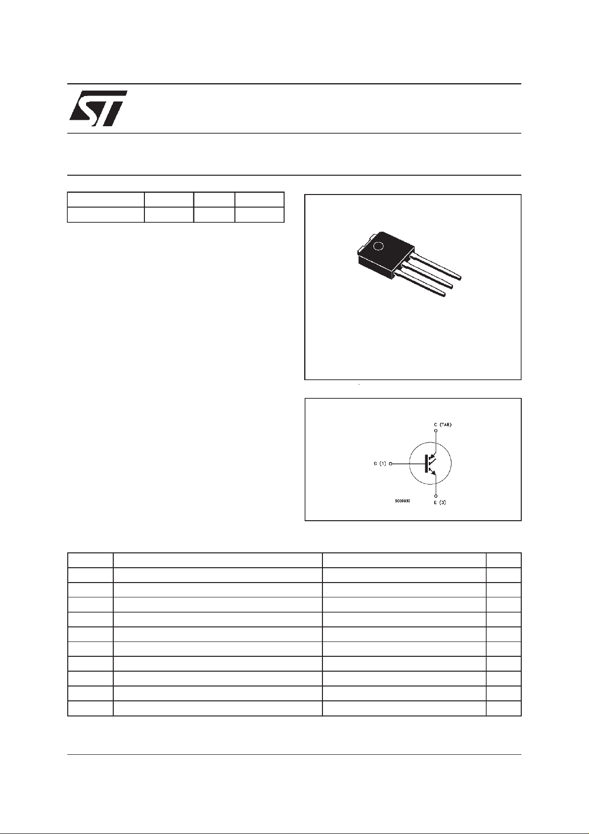
2
1
IPAK
TO-251
(Suffix ”-1”)
INTERNAL SCHEMATIC DIAGRAM
ABSOLUTE MAXIMUM RATINGS
Symb o l Parameter Value Unit
V
V
V
I
CM
P
T
(•) Pulsewidth limited by safeoperating area
June 1999
Collect o r -Em i t t er Volt age (VGS= 0) 600 V
CES
Emit t er-Collect or Volt age 20 V
ECR
Gate-Emitter V oltage
GE
I
Collect o r Current (cont inuous) at Tc=25oC14A
C
I
Collect o r Current (cont inuous) at Tc= 100oC7A
C
20 V
±
(•) Collecto r Current (pulsed) 56 A
Tot al Dissipation at Tc=25oC55W
tot
Derat ing F ac tor 0.44 W/
Sto rage Temperatur e -65 t o 150
stg
T
Max. Operating J unction T emperatur e 150
j
o
C
o
C
o
C
1/8
Page 2
STGD7NB60H-1
THERMAL DATA
R
thj-case
R
thj-amb
R
thc-sink
Ther mal Resistanc e Junct ion-case Max
Ther mal Resistanc e Junct ion-ambient Max
Ther mal Resistanc e Case-sink Ty p
2.27
100
1.5
o
C/W
o
C/W
o
C/W
ELECTRICAL CHARACTERISTICS
=25oC unless otherwise specified)
(T
j
OFF
Symbol Parameter Test Conditions Min. Typ. Max. Unit
V
BR(CES)
Collector-Emitter
IC=250µAVGE= 0 600 V
Break dow n Vo lt age
I
I
CES
GES
Collect o r c ut - off
=0)
(V
GE
Gat e- Em i t t er Leakage
Current (V
CE
=0)
V
=MaxRating Tj=25oC
CE
=MaxRating Tj=125oC
V
CE
V
= ± 20 V VCE=0 ±100 nA
GE
10
100
ON(∗)
Symbol Parameter Test Conditions Min. Typ. Max. Unit
V
GE(th)
Gate Th reshold
VCE=VGEIC= 250 µ A35V
Voltage
V
CE(SAT)
Collector-Emitter
Sat urat ion V olt age
VGE=15V IC=7A
V
=15V IC=7A Tj=125oC
GE
2.3
1.9
2.8 V
DYNAMIC
Symbol Parameter Test Conditions Min. Typ. Max. Unit
C
C
C
Q
Q
g
Q
I
CL
Forward
fs
Tr ansc on duc tance
Input Capaci t ance
ies
Out put Capac it anc e
oes
Reverse Transfer
res
Capacit a nc e
Tot al Gate Charge
G
Gate-Emitt er C harge
GE
Gat e- Col lect or C har ge
GC
Latc hing Cur rent V
VCE=25 V IC=7A 3.5 5 S
VCE=25V f=1MHz VGE= 0 390
45
10
VCE= 480 V IC=7A VGE=15V 42
560
68
15
730
90
20
55 nC
7.9
17.6
=480V RG=10Ω
clamp
T
= 150oC
j
28 A
µA
µ
V
pF
pF
pF
nC
nC
A
SWITCHINGON
Symbol Param et er Test Co n d i tions Mi n. Typ. Max. Uni t
(di/dt)
2/8
t
d(on)
E
Delay Time
t
Rise Time
r
Tur n-on Current Slope
on
Tur n-on Switc hing
on
Losses
VCC= 480 V IC=7A
=15V RG=10Ω
V
GE
VCC= 480 V IC=7A
=10Ω VGE=15V
R
G
T
= 125oC
j
15
48
160
70
ns
ns
A/µs
J
µ
Page 3
STGD7NB60H-1
ELECTRICAL CHARACTERISTICS
(continued)
SWITCHINGOFF
Symbol Parameter Test Conditions Min. Typ. Max. Unit
t
tr(v
(off)
t
d
E
off
E
t
tr(v
(off)
t
d
E
off
E
(•) Pulse width limited by max. junction temperature
(∗) Pulsed: Pulse duration = 300 µs, duty cycle 1.5%
(**)Losses Include Also The Tail (Jedec Standardization)
Cross-Over Time
c
Off Voltage Rise Time
)
off
Delay Time
t
Fall T ime
f
(**)
Turn-off Switching Loss
Tot al Switching Los s
ts
Cross-Over Time
c
)
Off Voltage Rise Time
off
Delay Time
t
Fall T ime
f
(**)
Turn-off Switching Loss
Tot al Switching Los s
ts
VCC = 480 V IC=7A
R
GE
=10
Ω
VGE=15V
VCC = 480 V IC=7A
R
GE
= 125oC
T
j
=10
Ω
VGE=15V
85
20
75
70
85
130
150
50
110
110
220
290
ns
ns
ns
ns
µJ
µ
ns
ns
ns
ns
µ
µ
J
J
J
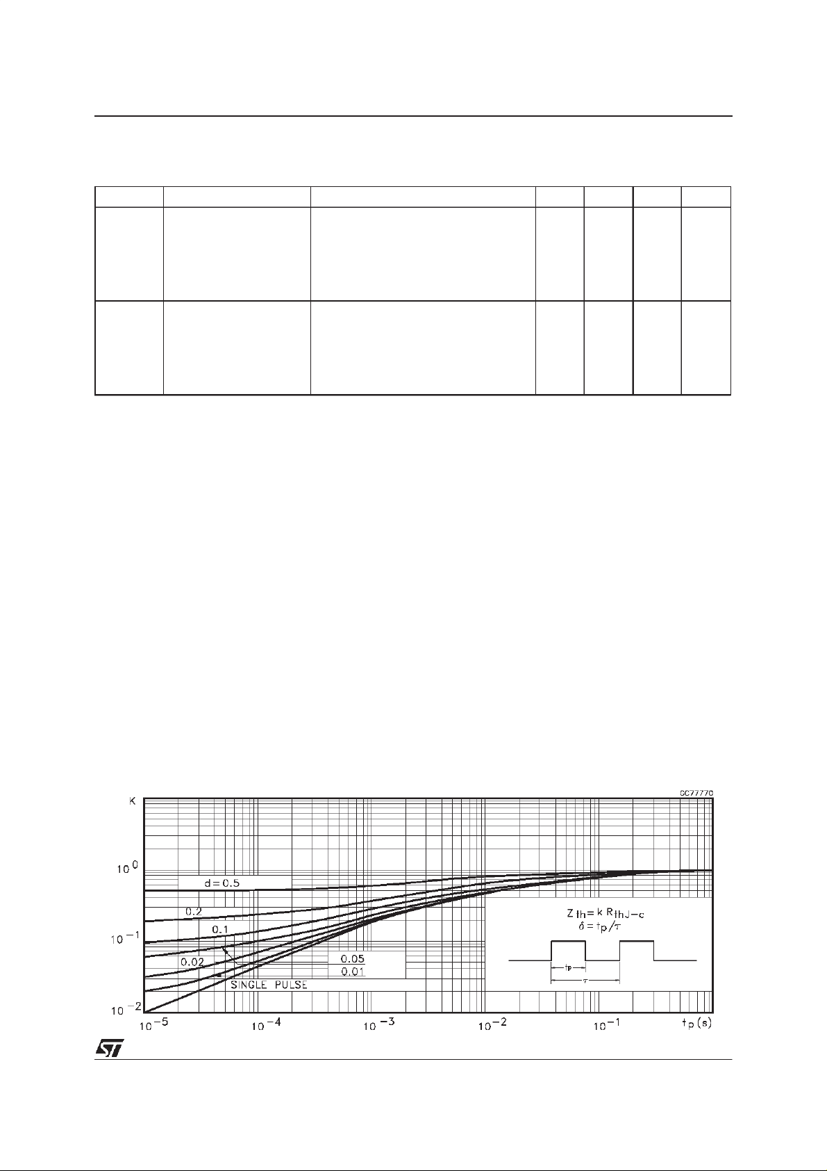
ThermalImpedance
3/8
Page 4

STGD7NB60H-1
OutputCharacteristics
Transconductance
TransferCharacteristics
Collector-EmitterOnVoltagevs Temperature
Collector-EmitterOnVoltagevs Collector Current
4/8
Gate Thresholdvs Temperature
Page 5

STGD7NB60H-1
NormalizedBreakdown Voltage vs Temperature
Gate Chargevs Gate-EmitterVoltage
CapacitanceVariations
TotalSwitchingLossesvs Gate Resistance
TotalSwitchingLossesvs Temperature
TotalSwitchingLossesvs Collector Current
5/8
Page 6

STGD7NB60H-1
SwitchingOff SafeOperatingArea
Fig. 1:
Gate Charge test Circuit
Fig. 3: Switching Waveforms
Fig. 2:
TestCircuitFor Inductive LoadSwitching
6/8
Page 7

TO-251 (IPAK) MECHANICALDATA
STGD7NB60H-1
DIM.
mm inch
MIN. TYP. MAX. MIN. TYP. MAX.
A 2.2 2.4 0.086 0.094
A1 0.9 1.1 0.035 0.043
A3 0.7 1.3 0.027 0.051
B 0.64 0.9 0.025 0.031
B2 5.2 5.4 0.204 0.212
B3 0.85 0.033
B5 0.3 0.012
B6 0.95 0.037
C 0.45 0.6 0.017 0.023
C2 0.48 0.6 0.019 0.023
D 6 6.2 0.236 0.244
E 6.4 6.6 0.252 0.260
G 4.4 4.6 0.173 0.181
H 15.9 16.3 0.626 0.641
L 9 9.4 0.354 0.370
L1 0.8 1.2 0.031 0.047
L2 0.8 1 0.031 0.039
A
E
==
C2
L2
B2
==
H
C
A3
A1
B6
L
B
B5
G
==
D
B3
2
13
L1
0068771-E
7/8
Page 8

STGD7NB60H-1
Information furnished is believedtobeaccurateand reliable.However, STMicroelectronics assumesno responsibility forthe consequences
of use of such information nor for any infringement of patents or other rights of third parties which may resultfrom its use. No license is
granted by implication orotherwise under any patent or patentrights of STMicroelectronics. Specificationmentioned in this publicationare
subjecttochange without notice.Thispublicationsupersedes andreplacesall information previously supplied. STMicroelectronics products
are not authorized for use as critical components in life support devicesor systems without expresswritten approval of STMicroelectronics.
The ST logo is a trademark of STMicroelectronics
1999STMicroelectronics – Printed in Italy – All Rights Reserved
STMicroelectronics GROUP OF COMPANIES
Australia - Brazil - China- Finland - France - Germany - Hong Kong - India - Italy - Japan - Malaysia - Malta - Morocco -
8/8
Singapore - Spain - Sweden - Switzerland - United Kingdom - U.S.A.
http://www.st.com
.
 Loading...