

Page 1

查询STGP20NC60V供应商
STGP20NC60V
STGW20NC60V
N-CHANNEL 30A - 600V - TO-220/TO-247
Very Fast PowerMESH™ IGBT
Table 1: Ge neral Features
TYPE V
STGP20NC60V
STGW20NC60V
■ OFF LOSSES INCLUDE TAIL CURRENT
■ LOSSES INCLUDE DIODE RECOVERY
CESVCE(sat)
600 V
600 V
(Max)
@25°C
< 2.5 V
< 2.5 V
I
C
@100°C
30 A
30 A
ENERGY
■ HIGH CURRENT CAPABILITY
■ HIGH FREQUENCY OPERATION UP TO 50
KHz
■ LOWER C
■ NEW GENERATION PRODUCTS WITH
RES
/ C
IES
RATIO
TIGHTER PARAMETER DISTRUBUTION
DESCRIPTION
Using the latest high voltage technology based on
a patented strip layout, STMicroelectronics has
designed an advanced family of IGBTs, the PowerMESH
™
IGBTs, with outstanding performances.
The suffix “V” identifies a family optimized for high
frequency.
Figure 1: Package
3
2
1
TO-220
TO-247
Weight for TO-220: 1.92gr ± 0.01
Weight for TO-247: 4.41gr ± 0.01
Max Clip Pressure: 150 N/mm
2
Figure 2: Internal Schematic Diagram
3
2
1
APPLICATIONS
■ HIGH FREQUENCY INVERTERS
■ SMPS and PFC IN BOTH HARD SWITCH AND
RESONANT TOPOLOGIES
■ UPS
■ MOTOR DRIVERS
Table 2: Order Codes
SALES TYPE MARKING PACKAGE PACKAGING
STGP20NC60V GP20NC60V TO-220 TUBE
STGW20NC60V GW20NC60V TO-247 TUBE
Rev. 4
1/11July 2004
Page 2

STGP20NC60V - STGW20NC 60V
Table 3: Absolute Maximum ratings
Symbol Parameter Value Symbol
V
CES
V
ECR
V
GE
I
C
I
C
I
(1)
CM
P
TOT
T
stg
T
j
(1)Pulse width limited by max. junction temperature.
Collector-Emitter Voltage (VGS = 0)
600
Reverse Battery Protection 20
Gate-Emitter Voltage ± 20
Collector Current (continuous) at 25°C (#) 60
Collector Current (continuous) at 100°C (#) 30
Collector Current (pulsed) 100 A
Total Dissipation at TC = 25°C
200
Derating Factor 1.6 W/°C
Storage Temperature
Operating Junction Temperature
– 55 to 150 °C
V
V
V
A
A
W
Table 4: Thermal Data
Min. Typ. Max.
Rthj-case Thermal Resistance Junction-case 0.625 °C/W
Rthj-amb Thermal Resistance Junction-ambient TO-220 62.5 °C/W
TO-247 50
T
L
Maximum Lead T emperature for Soldering
300 °C
Purpose (1.6 mm from case, for 10 sec.)
ELECTRICAL CHARACTERISTICS (T
=25°C UNLESS OTHERWISE SPECIFIED)
CASE
Table 5: Off
Symbol Parameter Test Conditions Min. Typ. Max. Unit
V
BR(CES)
Collectro-Emitter Breakdown
IC = 1 mA, VGE = 0 600 V
Voltage
I
CES
I
GES
Collector-Em itter Leak age
Current (V
CE
= 0)
Gate-Emitter Leakage
Current (V
CE
= 0)
V
= Max Rating
GE
Tc=25°C
Tc=125°C
V
= ± 20 V , VCE = 0 ± 100 nA
GE
10
1
Table 6: On
Symbol Parameter Test Conditions Min. Typ. Max. Unit
V
GE(th)
V
CE(SAT)
(#) Calculated according to the iterative formula:
Gate Threshold Voltage VCE= VGE, IC= 250 µA 3.75 5.75 V
Collector-Em itter Satur ation
Voltage
VGE= 15 V, IC= 20A, Tj= 25°C
VGE= 15 V, IC= 20A,
1.8
1.7
2.5 V
Tj= 125°C
µA
mA
V
ICTC()
2/11
T
–
--------------------------------------------------------------------------------------------------
=
R
THJ C–
JMAXTC
V
CESAT MAX()TCIC
,()×
Page 3

STGP20NC60V - STGW20NC60V
ELECTRICAL CHARACTERISTICS (CONTINUED)
Table 7: Dynamic
Symbol Parameter Test Conditions Min. Typ. Max. Unit
(1)
g
fs
C
ies
C
oes
C
res
Q
g
Q
ge
Q
gc
I
CL
Forward Transconductance
Input Capacitance
Output Capacitance
Reverse Transfer
Capacitance
Total Gate Charge
Gate-Emitter Charge
Gate-Collector Charge
Turn-Off SOA Minimum
Current
Table 8: Switching On
Symbol Parameter Test Conditions Min. Typ. Max. Unit
t
d(on)
t
r
(di/dt)
Eon (2)
t
d(on)
t
r
(di/dt)
Eon (2)
2) Eon is the turn-on losses when a typical diode is used in the test circuit in figure 2. If the IGBT is offered in a package with a co-pack diode,
the co-pack diode is us ed as external di ode. IGBTs & DIODE are at the same temperature (25°C and 125°C)
Turn-on Delay Time
Current Rise Time
Turn-on Current Slope
on
Turn-on Switching Losses
Turn-on Delay Time
Current Rise Time
Turn-on Current Slope
on
Turn-on Switching Losses
Table 9: Switching Off
Symbol Paramet er Test Conditions Min. Typ. Max . Unit
)
t
r(Voff
t
d(off
t
f
(3)
E
off
E
ts
t
r(Voff
t
d(off
t
f
E
(3)
off
E
ts
(3)Turn-off losses include al so the tail of the collector current.
Off Voltage Rise Time
)
Turn-off Delay Time 100 ns
Current Fall Time 75 ns
Turn-off Switching Loss 330 450
Total Switching Loss 550 750
)
Off Voltage Rise Time
)
Turn-off Delay Time 150 ns
Current Fall Time 130 ns
Turn-off Switching Loss 770
Total Switching Loss 1220
VCE = 15 V, IC= 20 A 15 S
= 25V, f = 1 MHz, VGE = 0 2200
V
CE
VCE = 390 V, IC = 20 A,
VGE = 15V,
(see Figure 20)
V
= 480 V , Tj = 150°C
clamp
100 A
225
50
100
16
45
140 nC
pF
pF
pF
nC
nC
RG = 10 Ω, VGE= 15V
= 390 V, IC = 20 A
V
CC
RG=3.3Ω, VGE= 15V, Tj= 25°C
(see Figure 18)
= 390 V, IC = 20 A
V
CC
RG=3.3Ω, VGE= 15V, Tj=
125°C
(see Figure 18)
Vcc = 390 V, IC = 20 A,
31
11
1600
220
300
31
11.5
1500
450
28 ns
ns
ns
A/µs
µJ
ns
ns
A/µs
µJ
RGE = 3.3 Ω , VGE = 15 V
TJ = 25 °C
(see Figure 18)
µJ
µJ
Vcc = 390 V, IC = 20 A,
= 3.3 Ω , VGE = 15 V
R
GE
Tj = 125 °C
(see Figure 18)
66 ns
µJ
µJ
3/11
Page 4

STGP20NC60V - STGW20NC 60V
Figure 3: Output Characteristics
Figure 4: Transconductance
Figure 6: Transfer Characteristics
Figure 7: Collector-Emitter On Voltage vs Temperature
Figure 5: Collector-Emitter On Voltage vs Collector Curre nt
4/11
Figure 8: Normalized Gate Threshold vs Temperature
Page 5
STGP20NC60V - STGW20NC60V
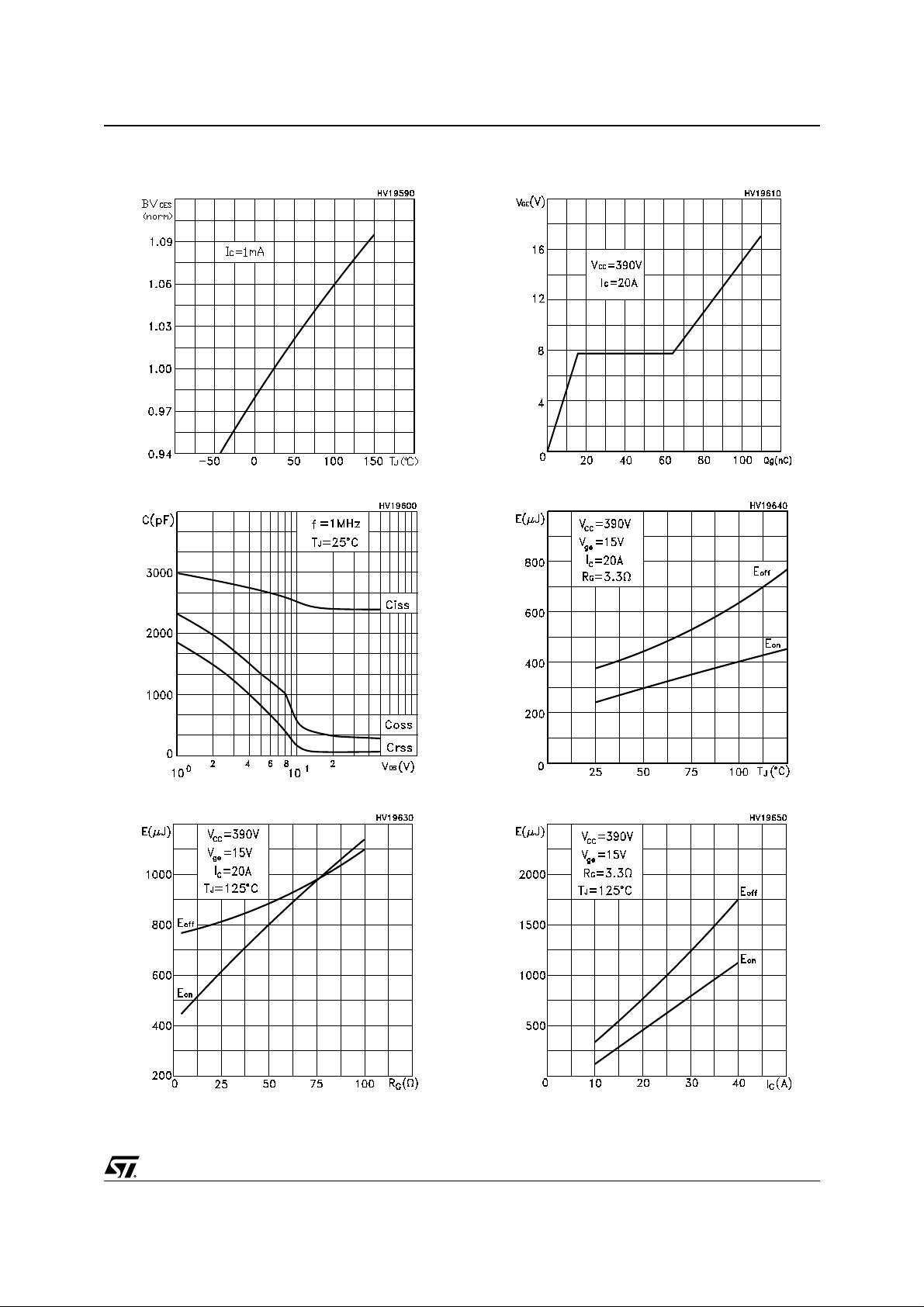
Figure 9: Normalized Breakdown Voltage vs
Temperature
Figure 10: Capacitance Variations
Figure 12: Gate Charge vs G ate-Emitter Voltage
Figure 13: Total Switching Lo sses vs Temp erature
Figure 11: Total Switching Losses vs Gate Resistance
Figure 14: Total Switching Losses vs Collector
Current
5/11
Page 6
STGP20NC60V - STGW20NC 60V
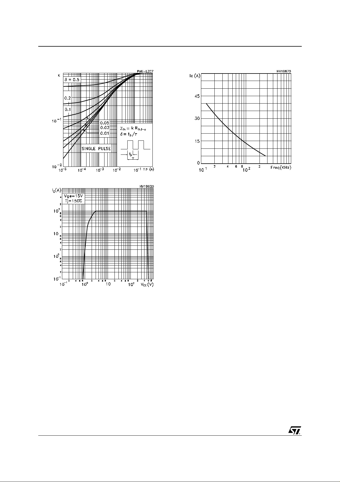
Figure 15: Thermal Impedance
Figure 16: Tur n-Off SO A
Figure 17: Ic vs Fr equency
For a fast IGBT suitable for high frequency applications, the typical collector current vs. maximum
operating frequency curve is reported. That frequency is defined as follows:
f
= (PD - PC) / (EON + E
MAX
OFF
)
1) The maximum power dissipation is limited by
maximum junction to case thermal resistance:
P
= ∆T / R
D
THJ-C
considering ∆T = TJ - TC = 125 °C- 75 °C = 50°C
2) The conduction losses are:
P
= IC * V
C
with 50% of duty cycle, V
CE(SAT)
* δ
typical value
CESAT
@125°C.
3) Power dissipation during ON & OFF commutations is due to the switching frequency:
P
= (EON + E
SW
OFF
) * freq.
4) Typical values @ 125°C for switching losse s are
used (test conditions: V
= 3.3 Ohm). Fu rthermore, diode recovery en-
R
G
ergy is included in the E
tail of the collector current is included in the E
= 390V, VGE = 15V,
CE
(see note 2), while the
ON
OFF
measurements (see note 3).
6/11
Page 7
STGP20NC60V - STGW20NC60V
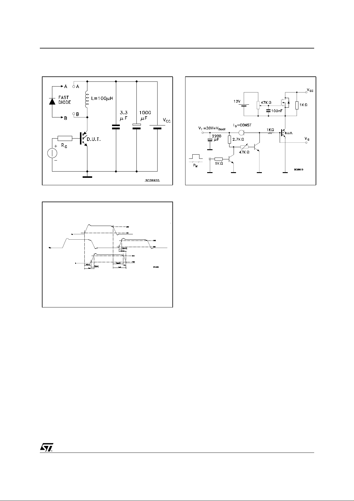
Figure 18: Test Circuit for Inductive Load
Swit c hing
Figure 19: Switching Waveforms
Figure 20: Gate Charge Test Circuit
7/11
Page 8
STGP20NC60V - STGW20NC 60V
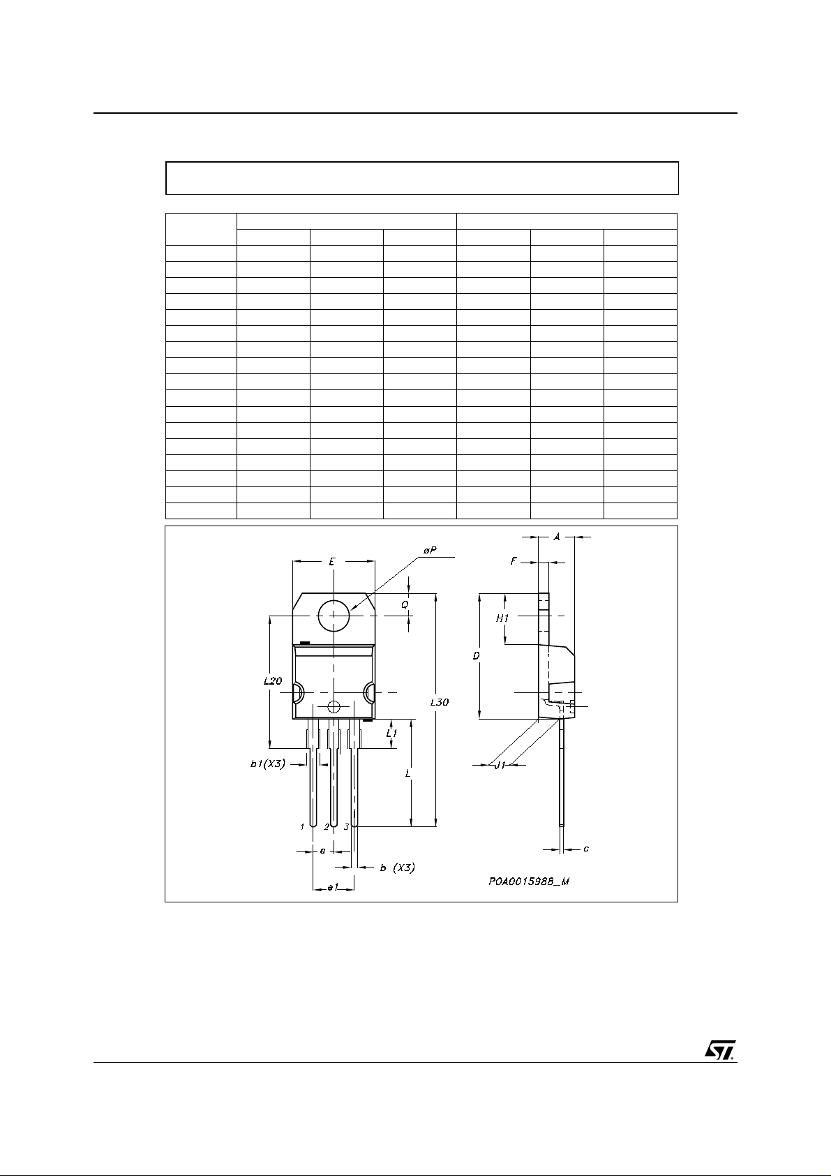
TO-220 MECHANICAL DATA
DIM.
A 4.40 4.60 0.173 0.181
b 0.61 0.88 0.024 0.034
b1 1.15 1.70 0.045 0.066
c 0.49 0.70 0.019 0.027
D 15.25 15.75 0.60 0.620
E 10 10.40 0.393 0.409
e 2.40 2.70 0.094 0.106
e1 4.95 5.15 0.194 0.202
F 1.23 1.32 0.048 0.052
H1 6.20 6.60 0.244 0.256
J1 2.40 2.72 0.094 0.107
L 13 14 0.511 0.551
L1 3.50 3.93 0.137 0.154
L20 16.40 0.645
L30 28.90 1.137
øP 3.75 3.85 0.147 0.151
Q 2.65 2.95 0.104 0.116
MIN. TYP MAX. MIN. TYP. MAX.
mm. inch
8/11
Page 9
STGP20NC60V - STGW20NC60V
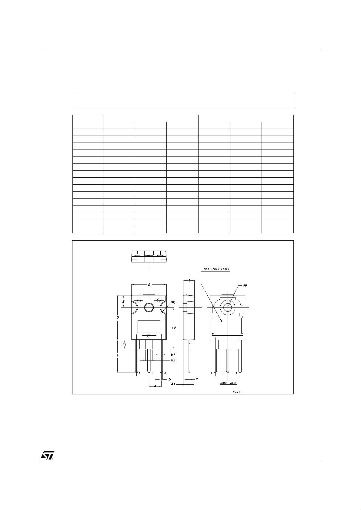
TO-247 MECHANICAL DATA
DIM.
A 4.85 5.15 0.19 0.20
A1 2.20 2.60 0.086 0.102
b 1.0 1.40 0.039 0.055
b1 2.0 2.40 0.079 0.094
b2 3.0 3.40 0.118 0.134
c 0.40 0.80 0.015 0.03
D 19.85 20.15 0.781 0.793
E 15.45 15.75 0.608 0.620
e5.45 0.214
L 14.20 14.80 0.560 0.582
L1 3.70 4.30 0.14 0.17
L2 18.50 0.728
øP 3.55 3.65 0.140 0.143
øR 4.50 5.50 0.177 0.216
S5.50 0.216
MIN. TYP MAX. MIN. TYP. MAX.
mm. inch
9/11
Page 10
STGP20NC60V - STGW20NC 60V
Table 10: Revision History
Date Revision Description of Change s
07-June-2004 4 Stylesheet update. No content change
10/11
Page 11

STGP20NC60V - STGW20NC60V
Information furnished is believed to be accurate and reliable. However, STMicroelectronics assumes no responsibility for the
consequences of use of such inform ation nor fo r an y infring ement of p atents or o ther rights of third p arties which may r esult f rom
its use. No license is granted by implication or otherwise under any patent or patent rights of STMicroelectronics. Specifications
mentioned in this publication are subject to change without notice. This publication supersedes and replaces all information
previously supplied. STMicroelectronics products are not authorized for use as critical components in life support devices or
systems without express written approval of STMicroelectronics.
Australia - Belgium - Brazil - Canada - China - Czech Republic - Finland - France - Germany - Hong Kong - India - Israel - Italy - Japan -
Malaysia - Malta - Morocco - Singapore - Spain - Sweden - Switzerland - United Kingdom - United States.
The ST logo is a registered trademark of STMicroelectronics
All other names are the property of their respective owners
© 2004 STMicroelectronics - All Rights Reserved
STMicroelectronics GROUP OF COMPANIES
11/11
 Loading...