

Page 1
N-CHANNEL 3A - 600V DPAK
TYPE V
CES
STGD3NB60SD 600 V < 1.5 V 3 A
■ HIGHINPUTIMPEDANCE
(VOLTAGEDRIVEN)
■ VERYLOW ON-VOLTAGEDROP (V
■ HIGHCURRENT CAPABILITY
■ OFFLOSSES INCLUDE TAIL CURRENT
■ INTEGRATEDFREEWHEELINGDIODE
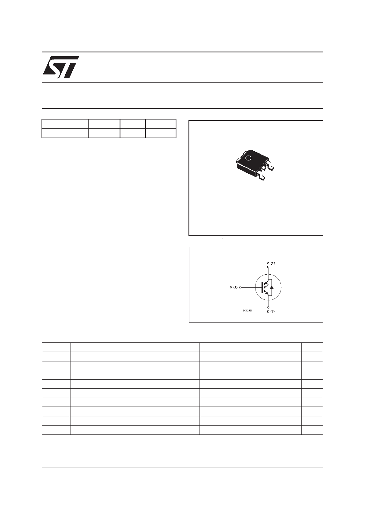
■ SURFACE-MOUNTINGDPAK (TO-252)
POWERPACKAGEIN TAPE & REEL
(SUFFIX”T4”)
DESCRIPTION
Using the latest high voltage technology based
on a patented strip layout, STMicroelectronics
has designed an advanced family of IGBTs, the
PowerMESH
IGBTs, with outstanding
perfomances. The suffix ”S” identifies a family
optimized to achieve minimum on-voltage drop
for low frequencyapplications(<1kHz).
V
CE(sat)
cesat
I
C
)
STGD3NB60SD
Power MESH IGBT
PRELIMINARY DATA
3
1
DPAK
TO-252
(Suffix ”T4”)
INTERNAL SCHEMATIC DIAGRAM
APPLICATIONS
■ GASDISCHARGELAMP
■ STATICRELAYS
■ MOTORCONTROL
ABSOLUTE MAXIMUM RATINGS
Symb o l Parameter Value Unit
V
V
I
CM
P
T
(•) Pulse width limited by safe operating area
Collect o r -Em i t t er Voltage (VGS= 0) 600 V
CES
Gate-Emitter Voltage ± 20 V
GE
I
Collect o r Current (continuo us) at Tc=25oC6A
C
I
Collect o r Current (continuo us) at Tc= 100oC3A
C
(•) Collect o r Current (pul s ed) 25 A
Tot al Dis sipation at Tc=25oC48W
tot
Derat ing Factor 0.32 W/
Sto rage Temperature -65 t o 17 5
stg
T
Max. O per a t ing J unction T emperat ur e 175
j
o
C
o
C
o
C
March 2000
1/8
Page 2
STGD3NB60SD
THERMAL DATA
R
thj-case
R
thj-amb
R
thc-sink
Ther mal Resistanc e Junct ion-case Max
Ther mal Resistanc e Junct ion-ambie nt Max
Ther mal Resistanc e Case-sink Ty p
3.125
100
1.5
o
C/W
o
C/W
o
C/W
ELECTRICAL CHARACTERISTICS
=25oC unless otherwisespecified)
(T
j
OFF
Symbol Parameter Test Conditions Min. Typ. M ax. Unit
V
BR(CES)
Collector-Emitter
IC=250µAVGE= 0 600 V
Break dow n Voltage
I
I
ON (∗
CES
GES
Collect o r cut-off
=0)
(V
GE
Gat e- Em i t t er Lea kage
Current (V
)
CE
=0)
V
=MaxRating Tj=25oC
CE
=MaxRating Tj=125oC
V
CE
V
= ± 20 V VCE=0 ±100 nA
GE
10
100
Symbol Parameter Test Conditions Min. Typ. M ax. Unit
V
GE(th)
Gate Threshold
VCE=VGEIC= 250 µA2.55V
Voltage
V
CE(SAT)
Collector-Emitter
Sat urat ion Voltage
VGE=15V IC=1.5A
V
=15V IC=3A
GE
=15V IC=3A Tj=125oC
V
GE
1
1.2
1.1
1.5
DYNAMIC
Symbol Parameter Test Conditions Min. Typ. M ax. Unit
C
C
C
Q
Q
g
Q
I
CL
Forward
fs
Tr ansc on duc tance
Input Capac i t ance
ies
Out put Capacitance
oes
Reverse Tr ansfer
res
Capacit a nc e
Tot al Gat e Charge
G
Gate-Emitt er Charge
GE
Gat e- Col lect or C harge
GC
Latc hing C ur rent V
VCE=25 V IC=3A 1.7 2.5 S
VCE=25V f=1MHz VGE= 0 255
30
5.6
330
40
7
VCE= 480 V IC=3A VGE=15V 18
5.4
5.5
=480V RG=1k
clamp
= 150oC
T
j
Ω
12 A
µA
µ
V
V
V
pF
pF
pF
nC
nC
nC
A
SWITCHINGON
Symbol Parameter Test Cond i tion s Min. T yp . Max. Unit
(di/dt)
2/8
t
d(on)
E
Delay T ime
t
Rise Ti me
r
Tur n-on Current Slop e
on
Tur n-on Switching
on
Losses
VCC= 480 V IC=3A
=15V RG=1kΩ
V
GE
VCC= 480 V IC=3A
R
=1k
G
= 125oC
T
j
Ω
VGE=15V
125
150
50
1100
ns
ns
A/µs
µJ
Page 3
STGD3NB60SD
ELECTRICAL CHARACTERISTICS
(continued)
SWITCHINGOFF
Symbol Parameter Test Conditions Min. Typ. M ax. Unit
tr(v
t
E
tr(v
t
E
t
c
d(off
t
off
t
c
d(off
t
off
Cross-Ov er Time
Off Voltage Rise Time
)
off
Delay T ime
)
Fall T ime
f
(**)
Turn-off Switching Loss
Cross-Ov er Time
Off Voltage Rise Time
)
off
Delay T ime
)
Fall T ime
f
(**)
Turn-off Switching Loss
V
=480V IC=3A
CC
R
=1k
Ω
=480V IC=3A
=1kΩ VGE=15V
= 125oC
V
R
T
GE
CC
GE
j
VGE=15V
1.8
1.0
3.4
0.72
1.15
2.8
1.45
3.6
1.2
1.8
COLLECTOR-EMITTER DIODE
Symbol Parameter Test Cond itions Mi n . Typ . Max. Unit
I
For ward Curre nt
f
I
V
t
Q
I
rrm
(•) Pulse width limited by max. junction temperature
(∗) Pulsed: Pulse duration = 300 µs, duty cycle 1.5 %
(**)Losses Include Also The Tail (Jedec Standardization)
For ward Curre nt pulsed
fm
For ward On-Voltage If=3A
f
Reverse Recovery Time
rr
Reverse Recovery Charge
rr
Reverse Recovery Current
=1A
I
f
If=3A VR=200 V
dI/dt = 100 A/ µ ST
= 125oC
j
1.55
1.15
1700
4500
9.5
3
25
1.9 V
µs
µ
µs
µ
mJ
µ
µs
µ
µ
mJ
s
s
s
s
s
A
A
V
ns
nC
A
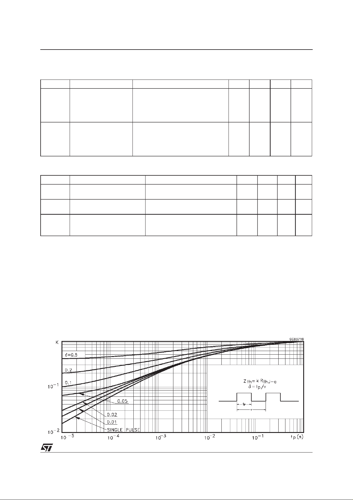
ThermalImpedance
3/8
Page 4

STGD3NB60SD
OutputCharacteristics
Transconductance
TransferCharacteristics
Collector-EmitterOn Voltage vs Temperature
Collector-EmitterOn Voltage vs Collector Current
4/8
Gate Threshold vs Temperature
Page 5

STGD3NB60SD
NormalizedBreakdownVoltagevs Temperature
Gate Chargevs Gate-EmitterVoltage
CapacitanceVariations
OffSwitching Losses vs Ic
OffSwitching Losses vs Tj
SwitchingOff Safe OperatinArea
5/8
Page 6

STGD3NB60SD
DiodeForwardvs Tj DiodeForward Voltage
Fig. 1: Gate Chargetest Circuit
Fig. 3: Switching Waveforms
Fig. 2: TestCircuit For InductiveLoad Switching
6/8
Page 7

TO-252 (DPAK) MECHANICAL DATA
STGD3NB60SD
DIM.
mm inch
MIN. TYP. MAX. MIN. TYP. MAX.
A 2.2 2.4 0.086 0.094
A1 0.9 1.1 0.035 0.043
A2 0.03 0.23 0.001 0.009
B 0.64 0.9 0.025 0.035
B2 5.2 5.4 0.204 0.212
C 0.45 0.6 0.017 0.023
C2 0.48 0.6 0.019 0.023
D 6 6.2 0.236 0.244
E 6.4 6.6 0.252 0.260
G 4.4 4.6 0.173 0.181
H 9.35 10.1 0.368 0.397
L2 0.8 0.031
L4 0.6 1 0.023 0.039
H
A
E
C2
L2
B2
==
==
DETAIL”A”
D
2
13
L4
A1
C
A2
DETAIL”A”
B
G
==
0068772-B
7/8
Page 8

STGD3NB60SD
Information furnishedis believedtobeaccurate and reliable.However, STMicroelectronics assumes no responsibilityforthe consequences
of use of such information nor for any infringement of patents or other rights of third parties which may result from its use. No license is
granted by implication or otherwise under any patent or patent rights of STMicroelectronics. Specificationmentioned in this publicationare
subjecttochange without notice.This publication supersedes andreplacesall information previouslysupplied.STMicroelectronics products
are not authorized for use as critical components in life support devices or systemswithout express written approval of STMicroelectronics.
The STlogo is a trademark of STMicroelectronics
1999 STMicroelectronics – Printed in Italy – All Rights Reserved
STMicroelectronics GROUP OF COMPANIES
Australia - Brazil - China - Finland - France - Germany - Hong Kong - India - Italy - Japan- Malaysia - Malta - Morocco -
8/8
Singapore - Spain - Sweden - Switzerland - United Kingdom - U.S.A.
http://www.st.com
.
 Loading...