

Page 1
STGB10NB37LZ
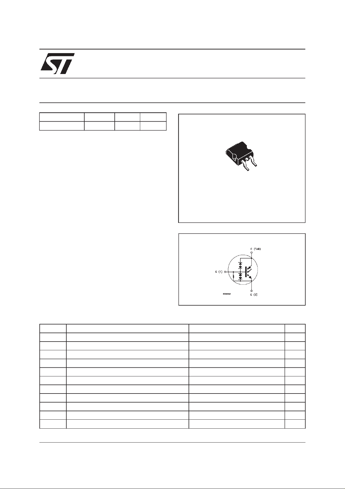
N-CHANNEL CLAMPED 10A D2PAK
INTERNALLYCLAMPED PowerMESH
TYPE V
ST G B10NB37LZ C LA MP ED < 1.8 V 10 A
■ POLYSILICONGATEVOLTAGE DRIVEN
■ LOW THRESHOLDVOLTAGE
■ LOW ON-VOLTAGEDROP
■ HIGHCURRENT CAPABILITY
■ HIGHVOLTAGECLAMPINGFEATURE
■ SURFACE-MOUNTINGD
CES
POWERPACKAGE IN TUBE (NO SUFFIX)
OR IN TAPE & REEL (SUFFIX ”T4”)
DESCRIPTION
Using the latest high voltage technology based
on patented strip layout, SGS-Thomson has
designed an advanced family of IGBTs with
outstandingperformances.
The built in collector-gate zener exhibits a very
precise active clamping while the gate-emitter
zenersuppliesan ESD protection.
APPLICATIONS
■ AUTOMOTIVEIGNITION
V
CE(sat)
2
PAK(TO-263)
I
C
IGBT
3
1
D2PAK
TO-263
INTERNAL SCHEMATIC DIAGRAM
ABSOLUTE MAXIMUM RATINGS
Symb o l Parameter Value Unit
V
V
V
I
CM
P
E
T
(•) Pulsewidth limited by safeoperating area
June 1999
Collect o r -Em i t t er Voltage ( VGS=0) CLAMPED V
CES
Reverse Bat tery P rotection 18 V
ECR
Gate-Emitter Voltage CLAMPED V
GE
I
Collect o r Current (con t inuous) at Tc=25oC20A
C
I
Collect o r Current (con t inuous) at Tc= 100oC20A
C
(•) Collect o r Current (pul sed) 60 A
Tot al Diss i pat ion at Tc=25oC 125 W
tot
Derat ing Factor 0.83 W/
ESD (Human Body M od el) 4 KV
SD
Sto rage Temperatur e - 65 to 175
stg
T
Max. O pera t ing J unc t ion T emperature 175
j
o
C
o
C
o
C
1/8
Page 2
STGB10NB37LZ
THERMAL DATA
R
thj-case
R
thj-amb
R
thc-sink
Ther mal Resistanc e Junct ion-case Max
Ther mal Resistanc e Junct ion-ambie nt Max
Ther mal Resistanc e Case-sink Ty p
1.2
62.5
0.2
o
C/W
o
C/W
o
C/W
ELECTRICAL CHARACTERISTICS
=25oC unless otherwise specified)
(T
j
OFF
Symbol Parameter Test Conditions Min. Typ. M ax. Unit
BV
BV
BV
I
I
(CES)
(ECR)
GE
CES
GES
Clamped Volt a ge IC= 2 mA VGE=0
=-40to150oC
T
j
Emitter C ollector
Break -down V oltage
Gate Emitter
Break -down V oltage
Collect o r cut-off
Current (VG E = 0)
Gat e- Em i t t er Leak age
IC=75mA VGE=0
=-40to150oC
T
j
IC=± 2mA
=-40to150oC
Τ
j
VCE=15V VGE=0 Tj=150oC
= 200 V VGE=0 Tj= 150oC
V
CE
VGE= ± 10 V VCE=0 ±0.7 mA
375 400 425 V
18 V
12 16 V
10
100
Current (VCE = 0)
R
Gate Emitter Resistance 20 K
GE
ON(∗)
Symbol Parameter Test Conditions Min. Typ. M ax. Unit
V
GE(th)
V
CE(SAT)
I
Gate Threshold
Voltage
Collector-Emitter
Sat urat ion Voltage
Collect o r Current VGE=4.5V VCE=9V 20 A
C
VCE=VGEIC= 250µA
=-40to150oC
T
j
VGE=4.5V IC=10A Tj=25oC
=4.5V IC=10A Tj=-40oC
V
GE
0.6 2.4 V
1.2
1.8 V
1.3
µ
µA
V
A
Ω
DYNAMIC
Symbol Parameter Test Conditions Min. Typ. M ax. Unit
g
C
C
C
Q
2/8
Forward
fs
VCE=25V IC= 10 A 10 18 S
Tr ansc on duc tance
Input Capaci t anc e
ies
Out put Capac it ance
oes
Reverse Tr ansfer
res
VCE=25V f=1MHz VGE= 0 1250
103
18
Capacit a nc e
Gat e Ch ar ge VCE= 320 V IC=10A VGE=5V 28 nC
G
1700
140
25
pF
pF
pF
Page 3
STGB10NB37LZ
FUNCTIONALCHARACTERISTICS
Symbol Parameter Test Conditions Min. Typ. M ax. Unit
II Lat ching C ur rent V
U.I.S. Unc lam pe d Ind uct ive
Switching Current
Func t ion al T e s t
AS
Single Pulse
E
Avalanc h e Energy
E
Revers e Avalanc he
AR
Energy
R
R
R
T
T
T
Tc=125oC duty cycle < 1 %
pulse width lim it ed by t
= 320 V VGE=5V
CLAM P
=1K
Ω
GOFF
=1 KΩ L = 200 µHTj=125oC
GOFF
=1 KΩ L=3mH
GOFF
=55oC
start
=55oC
start
=150oC
start
T
jmax
C
20 A
=125oC
15
12
215
150
10 mJ
A
A
mJ
mJ
ELECTRICAL CHARACTERISTICS
(continued)
SWITCHINGON
Symbol Parameter Test Conditions Min. Typ. M ax. Unit
t
d(on)
t
r
(di/dt)
E
on
Delay T im e
Rise Tim e
Tur n-on Current Slope
on
Turn-on
VCC= 320 V IC=10A
=5V RG=1KΩ
V
GE
VCC=320V IC=10A
R
=1K
G
Ω
VGE=5V
520
340
17
180
ns
ns
A/µs
µ
Switching Losses
SWITCHINGOFF
Symbol Parameter Test Conditions Min. Typ. M ax. Unit
t
tr(v
td(
E
off
t
tr(v
td(
E
off
(•) Pulse width limited by safe operatingarea (*) Pulsed: Pulse duration = 300 ms, duty cycle 1.5 % (**)LossesInclude Also TheTail(jedec Standardization)
Cross-Over T ime
c
Off Voltage Rise Time
)
off
Fall Time
t
f
Off Volt age Delay T im e
)
off
(**)
Turn-off Switching Loss
Cross-Over T ime
c
)
Off Voltage Rise Time
off
t
Fall Time
f
)
Off Volt age Delay T im e
off
(**)
Turn-off Switching Loss
V
R
V
R
T
=320V IC=10A
CLAM P
=1KΩ VGE=5V
GE
=320V IC=10A
CLAM P
=1KΩ VGE=5V
GE
= 125oC
j
4
2.2
1.5
14.8
4.0
5.2
2.8
2
15.8
6.5
µ
µs
µs
µs
mJ
µ
µs
µ
µs
mJ
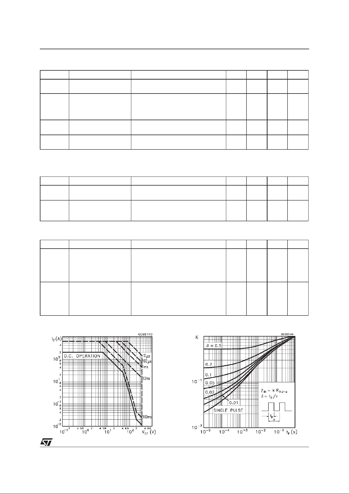
Safe OperatingArea Thermal Impedance
J
s
s
s
3/8
Page 4

STGB10NB37LZ
OutputCharacteristics
NormalizedGate ThresholdVoltage vs
Temperature
TransferCharacteristics
Transconductance
Collector-EmitterOn Voltagevs Temperature
4/8
Collector-EmitterOn Voltagevs Gate-Emitter
Voltage
Page 5

STGB10NB37LZ
CapacitanceVariations
OffLosses vs Gate Resistance
Gate Chargevs Gate-EmitterVoltage
OffLosses vs CollectorCurrent
Break-downVoltage vs Temperature
ClampingVoltage vs GateResistance
5/8
Page 6

STGB10NB37LZ
Fig. 1:
Fig. 3:
UnclampedInductive Load Test Circuit
SwitchingTimes Test Circuits For
ResistiveLoad
Fig. 2:
Fig. 4:
UnclampedInductive Waveform
GateCharge test Circuit
Fig. 5: Test Circuit For Inductive Load Switching
AndDIode RecoveryTimes
6/8
Page 7

TO-263 (D2PAK) MECHANICAL DATA
STGB10NB37LZ
DIM.
MIN. TYP. MAX. MIN. TYP. MAX.
A 4.4 4.6 0.173 0.181
A1 2.49 2.69 0.098 0.106
B 0.7 0.93 0.027 0.036
B2 1.14 1.7 0.044 0.067
C 0.45 0.6 0.017 0.023
C2 1.21 1.36 0.047 0.053
D 8.95 9.35 0.352 0.368
E 10 10.4 0.393 0.409
G 4.88 5.28 0.192 0.208
L 15 15.85 0.590 0.624
L2 1.27 1.4 0.050 0.055
L3 1.4 1.75 0.055 0.068
mm inch
D
A
C2
DETAIL”A”
C
A2
DETAIL”A”
A1
B2
E
L2
L
L3
B
G
P011P6/E
7/8
Page 8

STGB10NB37LZ
Information furnished is believedto beaccurate and reliable.However, STMicroelectronics assumesno responsibilityfor the consequences
of use of such information nor for any infringement of patents or other rights of third parties which may result from its use. No license is
granted by implication or otherwise under any patent or patent rights of STMicroelectronics. Specification mentioned in this publicationare
subjectto change without notice.This publication supersedes and replaces all information previouslysupplied. STMicroelectronics products
are not authorized for use as critical components in life support devices or systemswithout express written approval of STMicroelectronics.
The ST logo is a trademark of STMicroelectronics
1999STMicroelectronics – Printed in Italy – All Rights Reserved
STMicroelectronics GROUP OF COMPANIES
Australia - Brazil - China - Finland - France - Germany - Hong Kong - India - Italy - Japan - Malaysia - Malta - Morocco -
8/8
Singapore - Spain - Sweden - Switzerland - United Kingdom - U.S.A.
http://www.st.com
.
 Loading...