

Page 1
STGB10N60L
N-CHANNEL 10A - 600V D2PAK
LOGIC LEVEL IGBT
TYPE V
CES
V
CE(sat)
I
ST G B10N60L 600 V < 1. 95 V 10 A
■ HIGHINPUT IMPEDANCE
(VOLTAGEDRIVEN)
■ VERYLOWON-VOLTAGEDROP(V
■ LOW THRESHOLD VOLTAGE
cesat
(LOGICLEVEL INPUT)
■ HIGHCURRENTCAPABILITY
■ OFFLOSSESINCLUDETAILCURRENT
■ SURFACE-MOUNTINGD2PAK (TO-263)
POWERPACKAGEIN TUBE (NO SUFFIX)
OR IN TAPE & REEL (SUFFIX ”T4”)
APPLICATIONS
■ ELECTRONICIGNITION
■ LIGHT DIMMER
■ STATICRELAYS
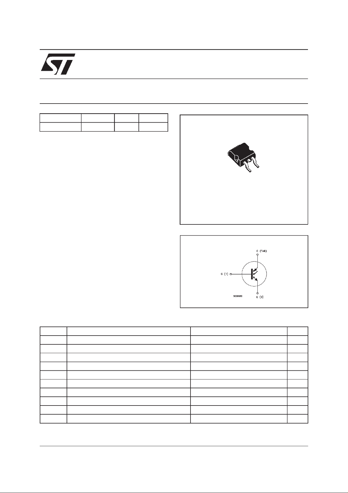
C
)
3
1
D2PAK
TO-263
INTERNAL SCHEMATIC DIAGRAM
ABSOLUTE MAXIMUM RATINGS
Symb o l Parameter Value Unit
V
V
V
I
CM
P
T
(•) Pulsewidth limited by safe operating area
June 1999
Collect o r -Em i t t er Volt age (VGS= 0) 600 V
CES
Reverse Battery Protection 25 V
ECR
Gate-Emitter V oltage
GE
I
Collect o r Current (con t inuo us ) at Tc=25oC25A
C
I
Collect o r Current (con t inuo us ) at Tc= 100oC20A
C
15 V
±
(•) Collect o r Current (pul sed) 100 A
Tot al Dis si pat ion at Tc=25oC 125 W
tot
Derat ing Fact or 0.83 W/
Sto rage Temper at ure -65 t o 175
stg
T
Max. O perating Junc t ion Temperat ure 175
j
o
C
o
C
o
C
1/8
Page 2
STGB10N60L
THERMAL DATA
R
thj-case
R
thj-amb
R
thc-sink
Ther mal Resistanc e Junct ion-case Max
Ther mal Resistanc e Junct ion-ambient Max
Ther mal Resistanc e Case-sink Ty p
1.2
62.5
0.1
o
C/W
o
C/W
o
C/W
ELECTRICAL CHARACTERISTICS
= - 40 to 150oC unlessotherwisespecified)
(T
j
OFF
Symbol Parameter Test Conditions Min. Typ. M ax. U nit
V
BR(ces)
Collector-Emitter
IC=250µAVGE= 0 600 V
Break dow n V o lt age
I
I
CES
GES
Collect o r cut-off
=0)
(V
GE
Gat e- Em i t t er Leak age
Current (V
CE
=0)
V
=MaxRating Tj=25oC
CE
=MaxRating Tj=125oC
V
CE
V
= ± 15 V VCE=0 ±100 nA
GE
25
100
ON(∗)
Symbol Parameter Test Conditions Min. Typ. M ax. U nit
V
GE(th)
V
CE(SAT)
I
Gate Th reshold
Voltage
Collector-Emitter
Sat urat ion Voltage
Collect o r Current VGE=4.5V VCE=7V 15 45 A
C
VCE=VGEIC= 250 µA
V
CE=VGEIC
=250µATj=25oC
VGE=4.5V IC=8A Tj=-40oC
=4.5V IC=9.5A Tj=25oC
V
GE
=4.5V IC=8A Tj= 150oC
V
GE
0.6
1.0
1.5
1.4
1.25
2.4
2.0
2.0
DYNAMIC
µ
µA
V
V
V
V
V
A
Symbol Parameter Test Conditions Min. Typ. M ax. U nit
g
Forward
fs
VCE=25 V IC=8A Tj=25oC7 12 S
Tr ansc on duc tance
C
ies
C
oes
C
res
Input Capacitance
Out put Capacitance
Reverse Tr ansfer
VCE=25V f=1MHz VGE= 0 1800
120
19
2600
165
26
Capacit a nc e
Q
Gat e Charge VCE= 400 V IC=8A VGE=5V 30 nC
G
FUNCTIONALCHARACTERISTICS
Symbol Parameter Test Conditions Min. Typ. M ax. U nit
2/8
I
CL
E
E
Latc hing C ur r ent V
For ward Clamping
CF
Energy
Revers e Avalanche
AR
= 480 V dV/ dt = 200 V/µs
clamp
= 125oC
T
j
T
=55oCV
start
= 10 A L = 4 .2 mH - Single Pul s e
I
C
clamp
=480V
Energy
20 A
210 mJ
10 mJ
pF
pF
pF
Page 3
STGB10N60L
ELECTRICAL CHARACTERISTICS
(continued)
SWITCHINGON
Symbol Parameter Test Conditions Min. Typ. M ax. U nit
t
d(on)
(di/dt)
E
Delay T ime
Rise Ti me
t
r
Tur n-on Current Slope
on
Turn-on
on
VCC= 480 V IC=8A
V
=5V RG=1K
GE
VCC=480V IC=8A
=1K
R
G
=125oC
T
j
Ω
VGE=5V
Ω
0.7
1.9
5
2.5
Switching Losses
SWITCHINGOFF
Symbol Parameter Test Conditions Min. Typ. M ax. U nit
t
tr(v
E
off
t
tr(v
E
off
(•)Pulse width limited by safe operatingarea
(∗) Pulsed: Pulse duration= 300µs, duty cycle 1.5%
(**)Losses Include AlsoThe Tail(Jedec Standardization)
Cross-Over Time
c
Off Voltage Rise Time
)
off
Fall T ime
t
f
(**)
Turn-off Switching Loss
Cross-Over Time
c
Off Voltage Rise Time
)
off
Fall T ime
t
f
(**)
Turn-off Switching Loss
V
=480V IC=8A
CC
=1KΩ VGE=5V
R
GE
T
=25oC
j
V
=480V IC=8A
CC
=1KΩ VGE=5V
R
GE
= 125oC
T
j
4
2.5
1.5
9.0
6
3.3
2.5
10.8
µs
s
µ
A/µs
mJ
s
µ
µs
s
µ
mJ
s
µ
µs
s
µ
mJ
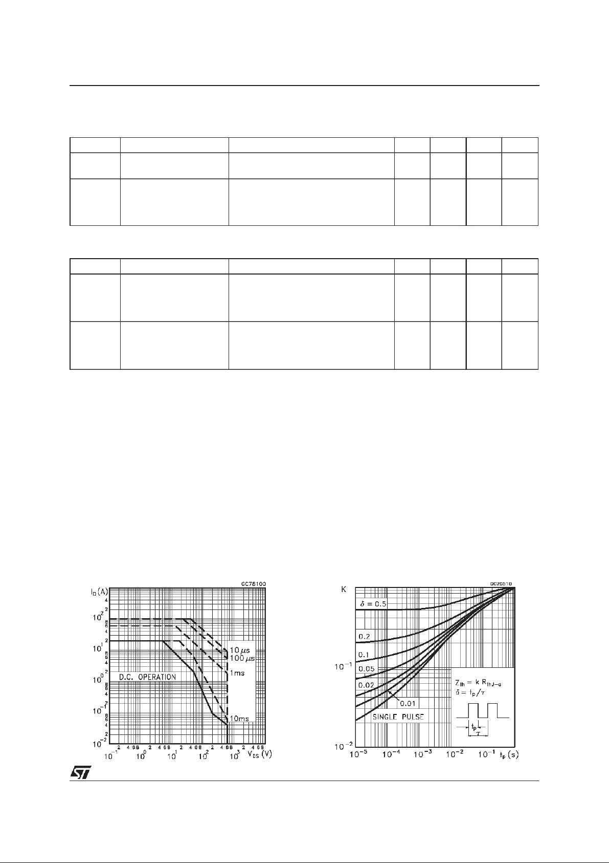
SafeOperatingArea ThermalImpedance
3/8
Page 4

STGB10N60L
OutputCharacteristics
Transconductance
TransferCharacteristics
Collector-EmitterOnVoltagevs Temperature
Collector-EmitterOnVoltagevs Collector
Current
4/8
CapacitanceVariations
Page 5

STGB10N60L
Gate Chargevs Gate-EmitterVoltage
Gate Thresholdvs Temperature
LatchingCurrent vs Rg
OffLossesvs CollectorCurrent
OffLossesvs GateResistance
OffLossesvs Temperature
5/8
Page 6

STGB10N60L
SwitchingOffSafeOperatinArea
Fig. 1: Gate Charge test Circuit Fig. 2: SwitchingTimesTest Circuit For
ResistiveLoad
Fig. 3:
6/8
Test Circuit For Inductive LoadSwitching
Page 7

TO-263 (D2PAK) MECHANICAL DATA
STGB10N60L
DIM.
MIN. TYP. MAX. MIN. TYP. MAX.
A 4.4 4.6 0.173 0.181
A1 2.49 2.69 0.098 0.106
B 0.7 0.93 0.027 0.036
B2 1.14 1.7 0.044 0.067
C 0.45 0.6 0.017 0.023
C2 1.21 1.36 0.047 0.053
D 8.95 9.35 0.352 0.368
E 10 10.4 0.393 0.409
G 4.88 5.28 0.192 0.208
L 15 15.85 0.590 0.624
L2 1.27 1.4 0.050 0.055
L3 1.4 1.75 0.055 0.068
mm inch
D
A
C2
DETAIL”A”
C
A2
DETAIL”A”
A1
B2
E
L2
L
L3
B
G
P011P6/E
7/8
Page 8

STGB10N60L
Information furnished is believedto be accurate and reliable.However, STMicroelectronics assumesno responsibility forthe consequences
of use of such information nor for any infringement of patents or other rights of third parties which may resultfrom its use. No license is
granted by implication or otherwise under any patent or patentrights ofSTMicroelectronics. Specification mentioned in this publication are
subjecttochange without notice.This publication supersedesand replaces all informationpreviously supplied. STMicroelectronics products
are not authorized for use as critical components in lifesupportdevices or systemswithout expresswritten approvalof STMicroelectronics.
The ST logo is a trademark of STMicroelectronics
1999 STMicroelectronics – Printed in Italy – All Rights Reserved
STMicroelectronics GROUP OF COMPANIES
Australia - Brazil - China - Finland - France - Germany - Hong Kong - India - Italy- Japan- Malaysia - Malta - Morocco -
8/8
Singapore - Spain - Sweden - Switzerland - United Kingdom - U.S.A.
http://www.st.com
.
 Loading...