

Page 1

Low voltage 0.5 Ω max, quad SPDT switch
Features
■ High speed:
–t
–t
■ Ultra low power dissipation:
–I
■ Low ON resistance V
–R
–R
–R
■ Wide operating voltage range:
–V
■ 4.3 V tolerant and 1.8 V compatible thresholds
on digital control input at V
■ Latch-up performance exceed 300 mA
(JESD 17)
■ ESD performance (analog chan. vs. GND):
HBM > 2 kV (MIL STD 883 method 3015)
Description
The STG3699B is a high-speed CMOS low
voltage quad analog SPDT (single-pole doublethrow) switch or 2:1 multiplexer/demultiplexer
switch fabricated using silicon gate C
technology. Designed to operate from 1.65 to
4.3 V, this device is ideal for portable applications.
= 1.5 ns (typ.) at VCC = 3.0 V
PD
= 1.5 ns (typ.) at VCC = 2.3 V
PD
=0.2μA (max.) at TA=85°C
CC
=0V:
IN
=0.50Ω (max. TA = 25°C) at
ON
V
=4.3V
CC
=0.55Ω (max. TA = 25°C) at
ON
V
=3.0V
CC
=0.55Ω (max. TA = 25°C) at
ON
V
=2.7V
CC
(OPR) = 1.65 to 4.3 V single supply
CC
= 2.3 to 3.0 V
CC
2
MOS
STG3699B
with break-before-make feature
QFN16L (2.6 x 1.8 mm)
It offers very low ON resistance (R
V
= 3.0 V. The nIN inputs are provided to
CC
control the independent channel switches nS1
and nS2. The switches nS1 ar e ON (connected to
common ports Dn) when the nIN input is held high
and OFF (state of high impedance ex ists between
the two ports) when nIN is held low. The switches
nS2 are ON (connected to common ports Dn)
when the nIN input is held low and OFF (state of
high impedance exists between the two ports)
when IN is held high. Additional key features are
fast switching speed, break-before-make delay
time and ultra low power consumption. All inputs
and outputs are equipped with protec tio n circ uits
against static discharge, giving them ESD and
excess transient voltage immunity.
The STG3699B is available in the commercial
temperature range of
-40to125°C in a QFN16L,
2.6 x 1.8 mm package.
<0.5Ω) at
ON
Table 1. Device summary
Order code Temperature range Package Packaging
STG3699BVTR –40 to 125°C QFN16L (2.6 x 1.8 mm) Tape and reel
September 2007 Rev 6 1/18
www.st.com
18
Page 2

Contents STG3699B
Contents
1 Summary description . . . . . . . . . . . . . . . . . . . . . . . . . . . . . . . . . . . . . . . . 3
1.1 Pin connection . . . . . . . . . . . . . . . . . . . . . . . . . . . . . . . . . . . . . . . . . . . . . . 3
2 Maximum rating . . . . . . . . . . . . . . . . . . . . . . . . . . . . . . . . . . . . . . . . . . . . . 5
3 DC and AC parameters . . . . . . . . . . . . . . . . . . . . . . . . . . . . . . . . . . . . . . . 6
4 Typical application . . . . . . . . . . . . . . . . . . . . . . . . . . . . . . . . . . . . . . . . . . 9
5 Test circuit . . . . . . . . . . . . . . . . . . . . . . . . . . . . . . . . . . . . . . . . . . . . . . . . 10
6 Wa veforms . . . . . . . . . . . . . . . . . . . . . . . . . . . . . . . . . . . . . . . . . . . . . . . . 11
7 Package mechanical data . . . . . . . . . . . . . . . . . . . . . . . . . . . . . . . . . . . . 14
8 Revision history . . . . . . . . . . . . . . . . . . . . . . . . . . . . . . . . . . . . . . . . . . . 17
2/18
Page 3

STG3699B Summary description
1 Summary description
1.1 Pin connection
Figure 1. Connections diagram (top through view)
CC
D1
16 15 14 13
1S1
V
4S2
1S2
1
1 - 2IN
2S1
2
STG3699B
3
D2
4
567
2S2
GND
3S1
Table 2. Pin description
Pin N° Symbol Name and function
15, 3, 7, 11,
1, 5, 9, 13
16, 4, 8, 12 D1 to D4 Common channels
2, 10 1-2IN, 3-4IN Input controls
14 V
6 GND Ground (0V)
1S1 to 4S1,
1S2 to 4S2
CC
Independent channels switches
Positiv e supply voltage
D4
12
4S1
11
3-4IN
10
9
3S2
8
D3
CS23251
3/18
Page 4

Summary description STG3699B
Figure 2. Input equivalent circuit
S2
S1
Table 3. Truth table
1-2IN 3-4IN ON switches
L - 1S2-D1, 2S2-D2
H - 1S1-D1, 2S1-D2
- L 3S2-D3, 4S2-D4
- H 3S1-D3, 4S1-D4
4/18
Page 5

STG3699B Maximum rating
2 Maximum rating
Stressing the device above the rating listed in the “Absolute maximum ratings” table may
cause permanent damage to the device. These are stress ratings only and operation of the
device at these or any ot her conditions above those indicated in the Operating sections of
this specification is not implied. Exposure to absolute maximum rating conditions for
extended periods may aff ect device reliability. Refer also to the STMicroelectronics SURE
Program and other relevant quality documents.
Table 4. Absolute maximum ratings
Symbol Parameter Value Unit
V
CC
V
V
V
I
IKC
I
IK
I
OK
I
O
I
OP
I
or I
CC
P
T
STG
T
1. Derate above 70°C: by 18.5mW/°C.
Supply voltage –0.5 to 5.5 V
DC input voltage –0.5 to VCC + 0.5 V
I
DC control input voltage –0.5 to 5.5 V
IC
DC output voltage –0.5 to VCC +0.5 V
O
DC input diode current on control pin (VIN<0V) –50 mA
DC input diode current (VIN<0V) ±50 mA
DC output diode current ±50 mA
DC output current ±300 mA
DC output current peak (pulse at 1 ms, 10% duty
cycle)
DC VCC or ground current ±100 mA
GND
Power dissipation at TA=70°C
D
(1)
±500 mA
1120 mW
Storage temperature –65 to 150 °C
Lead temperature (10 sec) 300 °C
L
Table 5. Recommended operating conditions
Symbol Parameter Value Unit
V
CC
V
I
V
IC
V
O
T
OP
dt/dv
Supply voltage (truth table guaranteed: 1.2 to 4.3 V) 1.65 to 4.3 V
Input voltage 0 to V
CC
V
Control input voltage 0 to 4.3 V
Output voltage 0 to V
CC
V
Operating temperature –55 to 125 ° C
= 1.65 to 2.7 V 0 to 20
V
Input rise and fall time control
input
CC
= 3.0 to 4.3 V 0 to 10
V
CC
ns/V
5/18
Page 6
DC and AC parameters STG3699B
3 DC and AC parameters
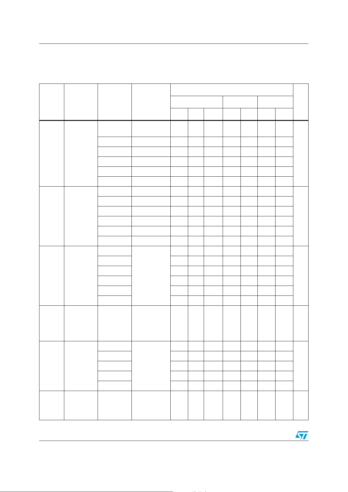
Table 6. DC specification
Value
Symbol Parameter
V
CC
(V)
Test
condition
= 25°C -40 to 85°C -55 to 125°C
A
Min Typ Max Min Max Min Max
UnitT
1.65–1.95
0.65
V
CC
0.65
V
CC
0.65
V
CC
2.3 – 2.5 1.2 1.2 1.2
IH
High level
input voltage
V
2.7 – 3.0 1.3 1.3 1.3
V
3.3 1.4 1.4 1.4
3.6 1.5 1.5 1.5
4.3 1.6 1.6 1.6
1.65 – 1.95 0.25 0.25 0.25
2.3 – 2.5 0.25 0.25 0.25
V
IL
Low level
input voltage
2.7 – 3.0 0.25 0.25 0.25
V
3.3 0.30 0.30 0.30
3.6 0.30 0.30 0.30
4.3 0.40 0.40 0.40
4.3
0.35 0.50 0.60
3.0 0.45 0.55 0.65
=0V to
V
2.7 0.45 0.55 0.65
2.3 0.45 0.70 0.80
ON
Switch ON
resistance
R
S
V
CC
IS= 100 mA
Ω
1.8 0.55 1.5 2.0
1.65 0.65 1.5 2.0
ON
ΔR
ON
resistance
match
between
channels
2.7
(1)
V
at R
S
ON
IS=100mA
max
4.3
R
FLAT
ON
resistance
flatness
(2)
3.0 0.20 0.25 0.25
2.7 0.20 0.25 0.25
2.3 0.20 0.25 0.25
=0V to
V
S
V
CC
IS=100mA
1.65 0.32 0.42 0.42
OFF state
I
OFF
leakage
current
4.3 V
= 0.3 or 4 V ±20 ±100 nA
S
(nSn), (Dn)
6/18
0.15 Ω
0.15 0.20 0.20
Ω
Page 7

STG3699B DC and AC parameters
Table 6. DC specification (continued)
Value
V
Symbol Parameter
CC
(V)
Input
I
leakage
IN
0–4.3 V
current
Quiescent
I
CC
supply
1.65 – 4.3
current
Quiescent
supply
I
CCLV
current low
4.3
voltage
driving
1. ΔRON=R
2. Flatness is defined as the difference between the maximum and minimum value of ON resistance as measured over the
specified analog signal ranges.
ON(Max)–RON(Min)
Test
condition
= 25°C -40 to 85°C -55 to 125°C
A
Min Typ Max Min Max Min Max
= 0 to 4.3V ±0.1 ±1 μA
IN
V
IN=VCC
GND
V
1-2IN,
V
3-4IN
V
1-2IN,
V
3-4IN
V
1-2IN,
V
3-4IN
or
=1.65V
=1.80V
= 2.60 V
±0.05 ±0.2 ±1 μA
±37 ±50 ±100
±33 ±40 ±50
±12 ±20 ±30
UnitT
μA
Table 7. AC electrical characteristics (CL=35pF, RL=50Ω, tr=tf ≤5ns)
Value
Symbol Parameter
t
PLH,tPHL
t
ON
t
OFF
Propagation
delay
Turn-ON time
Turn-OFF
time
V
CC
(V)
1.65 – 1.95
2.3 – 2.7 0.40
3.0 – 3.3 0.30
3.6 – 4.3 0.30
1.65 – 1.95 V
2.3–2.7
3.0 – 3.3 42 55 65
3.6 – 4.3 40 55 65
1.65 – 1.95 VS=0.8V 22
2.3–2.7
3.0 – 3.3 16 30 40
3.6 – 4.3 15 30 40
Test
condition
Min Typ Max Min Max Min Max
V
= OPEN
I
=0.8V 120
S
V
=1.5V
S
V
= 1.5 V
S
= 25°C -40 to 85°C -55 to 125°C
A
0.45
45 55 65
18 30 40
UnitT
ns
ns
ns
7/18
Page 8

DC and AC parameters STG3699B
Table 7. AC electrical characteristics (CL=35pF, RL=50Ω, tr=tf ≤5 ns) (continued)
Value
Symbol Parameter
V
CC
(V)
Test
condition
= 25°C -40 to 85°C -55 to 125°C
A
Min Typ Max Min Max Min Max
UnitT
53
t
D
Breakbefore- make
time delay
1.65 – 1.95
= 35 pF
C
2.3–2.7 28
3.0–3.3 12
L
= 50 Ω
R
L
VS = 1.5 V
3.6–4.3 8
1.65 – 1.95
=100 pF
C
Charge
Q
injection
2.3–2.7 48
3.0–3.3 48
3.6–4.3 57
L
RL= 1 MΩ
V
= 0 V
GEN
= 0 Ω
R
GEN
42
Table 8. Analog sw itch characteristics (CL= 5pF, RL=50Ω, TA=25° C)
Value
V
Symbol Parameter
OIRR
Off Isolation
(1)
CC
(V)
1.65 – 4.3
Xtalk Crosstalk 1.65 – 4.3
Total
THD
harmonic
2.3–4.3
distortion
BW
-3dB
Bandwidth
1.65 – 4.3 R
Control pin
C
input
IN
capacitance
Sn
Sn port
capacitance
3.3 f = 1 MHz 80
C
Test
condition
= 25°C -40 to 85°C -55 to 125°C
A
Min Typ Max Min Max Min Max
V
=1V
S
RMS
f=100kHz
=1 V
V
S
RMS
f=100kHz
= 600 Ω
R
L
VIN=2V
PP
f=20Hz to
–71 dB
–72 dB
0.03 %
20 kHz
= 50 Ω 40 MHz
L
5
ns
pC
UnitT
pF
D port
D
capacitance
when switch
3.3 f = 1 MHz 170
C
is enabled
1. Off-isolation = 20 log10 (VD/VS), VD = output, VS = input to off switch
8/18
Page 9

STG3699B Typical application
4 Typical application
Figure 3. ON resistance Figure 4. Bandwidth
Figure 5. OFF leakage Figure 6. Channel-to-channel crosstalk
Figure 7. OFF isolation
9/18
Page 10

Test circuit STG3699B
5 Test circuit
Figure 8. Test circuit
= 5/35 pF or equivalent (includes jig and probe capacitance)
C
L
R
=50Ω or equivalent
L
R
T=ZOUT
of pulse generator (typically 50 Ω)
10/18
Page 11

STG3699B Waveforms
6 Waveforms
Figure 9. Break-before-make time del ay
11/18
Page 12

Waveforms STG3699B
Figure 10. Switching time and charge injection (V
C
=100pF)
L
GEN
=0V, R
=0Ω, RL=1MΩ,
GEN
12/18
Page 13

STG3699B Waveforms
Figure 11. Turn ON, Turn OFF delay time
13/18
Page 14

Package mechanical data STG3699B
7 Package mechanical data
In order to meet environmental requ irements, ST offers these devices in ECOPACK®
packages. These packages have a Lead-free second level interconnect. The category of
second Level Interconnect is marked on the package and on the inner box label, in
compliance with JEDEC Standard JESD97. The maximum ratings related t o soldering
conditions are also marked on the inner box label. ECOPACK is an ST trademark.
ECOPACK specifications are available at: www.st.com.
Figure 12. QFN16L (2.6 x 1.8 mm) package outline
1. Drawing not to scale.
Table 9. QFN16L (2.6 x 1.8 mm) mechanical data
Symbol
Nom Min Max
A 0.55 0.45 0.60
A1 0.02 0 0.05
b 0.20 0.15 0.25
D 2.60 2.50 2.70
E 1.80 1.70 1.90
e 0.40
L 0.40 0.35 0.45
14/18
Dimensions
Databook (mm)
Page 15

STG3699B Pac kage mechanical data
Figure 13. Footprint recommendations
15/18
Page 16

Package mechanical data STG3699B
Figure 14. QFN16L (2.6 x 1.8 mm) tape & reel information
16/18
Page 17

STG3699B Revision history
8 Revision history
Table 10. Document revision history
Date Revision Changes
13-Oct-2005 1 First Release.
21-Dec-2005 2 Added tape & reel information.
17-Feb-2006 3 R
10-Aug-2006 4 New template, Table 1 updated.
19-Feb-2007 5 Updated OIRR, Xtalk valuers in Table 8 on page 8.
4-Sept-2007 6
updated it Table 6: DC specification on page 6
FLAT
Updated I
restructured layout.
value in Table 4 on page 5, small text changes,
OK
.
17/18
Page 18

STG3699B
Please Read Carefully:
Information in this document is provided solely in connection with ST products. STMicroelectronics NV and its subsidiaries (“ST”) reserve the
right to make changes, corrections, modifications or improvements, to this document, and the products and services described herein at any
time, without notice.
All ST products are sold pursuant to ST’s terms and conditions of sal e.
Purchasers are solely res ponsibl e fo r the c hoic e, se lecti on an d use o f the S T prod ucts and s ervi ces d escr ibed he rein , and ST as sumes no
liability whatsoever relati ng to the choice, selection or use of the ST products and services described herein.
No license, express or implied, by estoppel or otherwise, to any intellectual property rights is granted under this document. If any part of this
document refers to any third pa rty p ro duc ts or se rv ices it sh all n ot be deem ed a lice ns e gr ant by ST fo r t he use of su ch thi r d party products
or services, or any intellectua l property c ontained the rein or consi dered as a warr anty coverin g the use in any manner whats oever of suc h
third party products or servi ces or any intellectual property contained therein.
UNLESS OTHERWISE SET FORTH IN ST’S TERMS AND CONDITIONS OF SALE ST DISCLAIMS ANY EXPRESS OR IMPLIED
WARRANTY WITH RESPECT TO THE USE AND/OR SALE OF ST PRODUCTS INCLUDING WITHOUT LIMITATION IMPLIED
WARRANTIES OF MERCHANTABILITY, FITNESS FOR A PARTICUL AR PURPOS E (AND THEIR EQUIVALE NTS UNDER THE LAWS
OF ANY JURISDICTION), OR INFRINGEMENT OF ANY PATENT, COPYRIGHT OR OTHER INTELLECTUAL PROPERTY RIGHT.
UNLESS EXPRESSLY APPROVED IN WRITING BY AN AUTHORIZED ST REPRESENTATIVE, ST PRODUCTS ARE NOT
RECOMMENDED, AUTHORIZED OR WARRANTED FOR USE IN MILITARY, AIR CRAFT, SPACE, LIFE SAVING, OR LIFE SUSTAINING
APPLICATIONS, NOR IN PRODUCTS OR SYSTEMS WHERE FAILURE OR MALFUNCTION MAY RESULT IN PERSONAL INJ URY,
DEATH, OR SEVERE PROPERTY OR ENVIRONMENTAL DAMAGE. ST PRODUCTS WHICH ARE NOT SPECIFIED AS "AUTOMOTIVE
GRADE" MAY ONLY BE USED IN AUTOMOTIVE APPLICATIONS AT USER’S OWN RISK.
Resale of ST products with provisions different from the statements and/or technical features set forth in this document shall immediately void
any warranty granted by ST fo r the ST pro duct or serv ice describe d herein and shall not cr eate or exten d in any manne r whatsoever , any
liability of ST.
ST and the ST logo are trademarks or registered trademarks of ST in various countries.
Information in this document su persedes and replaces all info rmation previously supplied .
The ST logo is a registered trademark of STMicroelectronics. All other names are the property of their respective owners.
© 2007 STMicroelectronics - All rights reserved
STMicroelectronics group of compan ie s
Australia - Belgium - Brazil - Canada - China - Czech Republic - Finland - France - Germany - Hong Kong - India - Israel - Italy - Japan -
Malaysia - Malta - Morocco - Singapore - Spain - Sweden - Switzerland - United Kingdom - United States of America
www.st.com
18/18
 Loading...