

Page 1
LOW VOLTAGE 0.5/0.8Ω MAX DUAL SPDT SWITCH
WITH BREAK BEFORE MAKE FEATURE
■ HIGH SPEED:
t
= 0.3ns (TYP.) at VCC=3.0V
PD
t
= 0.4ns (TYP.) at VCC=2.3V
PD
■ ULTRA LOW POWER DISSIPATION:
I
=0.2µA (MAX.)at TA= 85°C
CC
■ LOW "ON" RESISTANCE V
R
R
■ WIDE OPERATING VOLTAGE RANGE:
V
■ 4.3V TOLERANT AND 1. 8V COMPATIBLE
=0.5Ω (MAX. TA= 25°C) at VCC=2.7V
ON-S1
=0.8Ω (MAX. TA= 25°C) at VCC=2.7V
ON-S2
(OPR) = 1.65V to 4.3V SINGLE SUPPLY
CC
THRESHOLD ON DIGITALCONTROL I NPUT
at V
■ LATCH-UP PERFORMANCE EXCEE DS
= 2.3 to 3. 0V
CC
300mA (JESD 17)
DESCRIPTION
The STG3680 is an high-speed CMOS DUAL
ANALOG S.P.D.T. (Single Pole Dual T hrow)
SWITCH or DUAL 2:1 Multiplexer/Demultiplexer
Bus Switch fabricated in silicon gate C
technology. It is designed t o operate from 1.65V to
4.3V, making this device ideal for portable
applications.
It o ffers very low ON-Resistance (<0.5
2S1 channels; <0.8
V
=2.7V. The nIN inputs are provided to control
CC
Ω 1S2 and 2S2 channels) at
the swi tches. The switches nS1 are ON (they are
IN
=0V:
2
MOS
Ω 1S1 and
STG3680
QFN
ORDER CODES
PACKAGE T & R
QFN STG3680QTR
connected to c ommon Ports Dn) w hen the nIN
input is held high and OFF (high impedance state
exists between the two ports) when nIN is held
low; the switches nS2 are ON (they are connected
to common Ports Dn) when the nIN input is held
low and OFF (high impedance state exists
between the two ports) when IN is held high.
Additional key features are fast switching speed,
Break Before Make Delay Time and Ultra Low
Power Consumption. All inputs and outp uts are
equipped with protection circuits against static
discharge, giving them ESD immunity a nd
transient excess voltage. It’s available in the
commercial temperature range in the QF N
package.
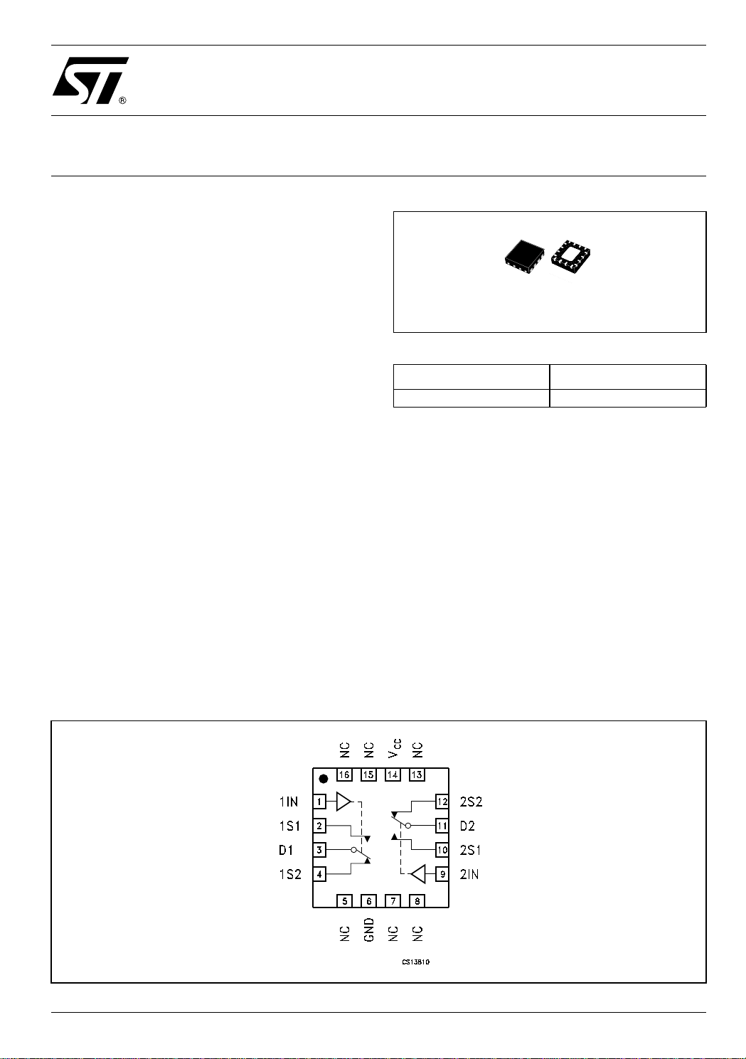
PIN CONNECTION
Rev. 3
1/11May 2004
Page 2
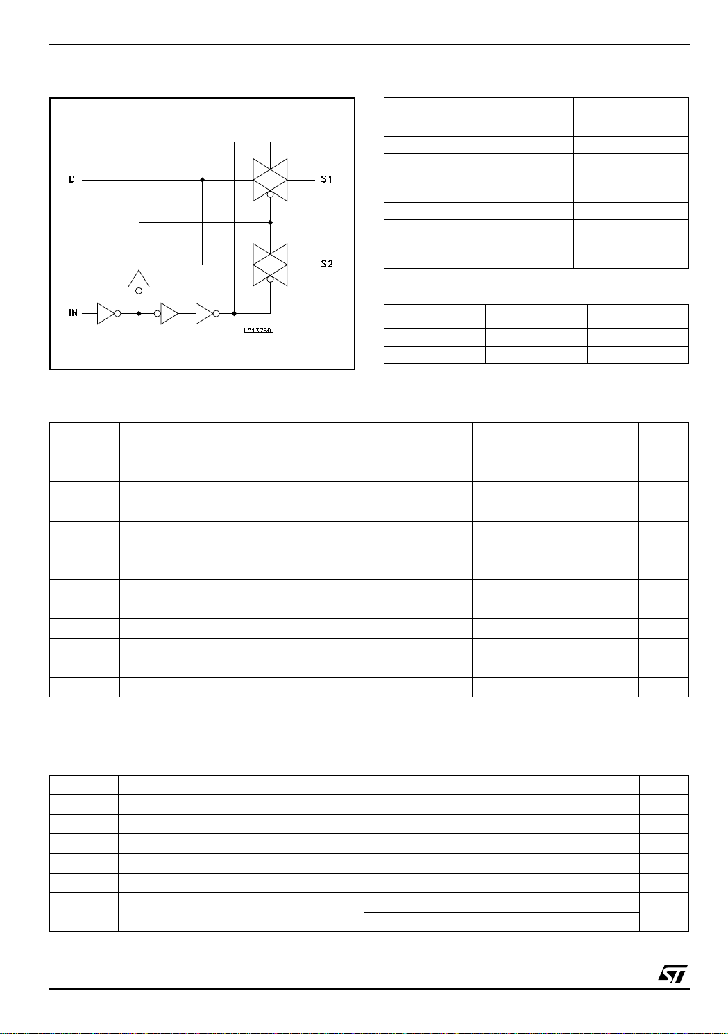
STG3680
Figure 1: Input Equivalent Circuit Table 1: Pin Description
QFN
PIN N°
SYMBOL
NAME AND
FUNCTION
1, 9 1IN, 2IN Controls
2, 10
4, 12
1S1 to 2S1
1S2 to 2S2
Independent Channels
3, 11 D1, D2 Common Channels
5,7,8,13,15,16 NC Not Connected
6 GND Ground (0V)
14 V
CC
PositiveSupply
Voltage
Table 2: Truth Table
IN SWITCH S1 SWITCH S2
H ON OFF(*)
L OFF(*) ON
(*) High Impedance
Table 3: Absolute Maximum Ratings
Symbol Parameter Value Unit
V
V
V
V
I
IKC
I
I
OK
I
I
OP
or I
I
CC
P
T
T
Absolute Maximum Ratings are those values beyond which damage to the device may occur. Functional operation under these conditions is
not implied.
(1) Derate above 70°C: by 18.5mW/°C.
Supply Voltage
CC
DC Input Voltage -0.5 to VCC+0.5
I
DC Control Input Voltage
IC
DC Output Voltage -0.5 to VCC+0.5
O
DC Input Diode Current on control pin (VIN<0V)
DC InputDiode Current (VIN<0V)
IK
DC Output Diode Current
DC Output Current
O
DC Output Current Peak (pulse at 1ms, 10% duty cycle)
DC VCCor Ground Current
GND
Power Dissipation at Ta=70°C (1)
D
Storage Temperature
stg
Lead Temperature (10 sec)
L
-0.5 to 4.6 V
V
-0.5 to 4.6 V
V
− 50 mA
± 50 mA
± 20 mA
± 300 mA
± 500 mA
± 100 mA
1120 mW
-65 to 150 °C
300 °C
Table 4: Recommended Operating Conditions
Symbol Parameter Value Unit
V
V
V
V
T
dt/dv
1) Truth Table guaranteed: 1.2V to 4.3V.
Supply Voltage (note 1)
CC
Input Voltage 0 to V
I
Control Input Voltage
IC
Output Voltage 0 to V
O
Operating Temperature
op
Input Rise and Fall Time Control Input V
= 1.65V to 2.7V
CC
V
= 3.0V to 4.3V
CC
1.65 to 4.3 V
CC
0to4.3 V
CC
-55 to 125 °C
0to20
0to10
2/11
V
V
ns/V
Page 3
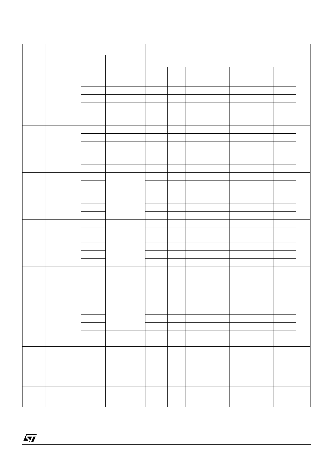
Table 5: DC Specifications
Test Conditions Value
Symbol Parameter
V
High Level
IH
Input Voltage
V
Low Level
IL
Input Voltage
R
ON-S1
Switch
ON-S1
Resistance
(1)
R
ON-S2
Switch
ON-S2
Resistance
(1)
∆R
ON
ON Resist.
Match
between
channels
(1, 2)
FLAT
ON
Resistance
R
FLATNESS
(3)
OFF State
I
OFF
Leakage
Current
(nSn), (Dn)
Input Leak.
I
IN
Current
I
Quiescent
CC
Supply
Current (1)
V
CC
(V)
1.65-1.95 0.65V
2.3-2.5
2.7-3.0
3.3 1.5
3.6
4.3
1.65-1.95 0.40 0.40 0.40
2.3-2.5
2.7-3.6
3.3 0.50 0.50 0.50
3.6
4.3 1.3 1.3 1.3
4.3
3.0 0.80 0.80
2.7 0.80 0.80
2.3 2 2
1.8 4.0 5.0
1.65 4.0 5.0
4.3
3.0 0.40 0.50 0.60
2.7 0.40 0.50 0.60
2.3 0.50 0.80 0.80
1.8 0.70 3.0 4.0
1.65 0.80 3.0 4.0
2.7
4.3
3.0
2.7 0.07 0.15 0.15
2.3
1.65 V
4.3
0-4.3 VIN=0to3.6V ±0.1 ± 1 µA
1.65-4.3 VIN=VCCor
STG3680
=25°C
T
A
Min. Typ. Max. Min. Max. Min. Max.
CC
1.4 1.4 1.4
1.4 1.4 1.4
1.7 1.7 1.7
2.2 2.2 2.2
0.50 0.50 0.50
0.50 0.50 0.50
0.50 0.50 0.50
0.80 0.80
=0V to V
V
S
CC
IS=100mA
0.40 0.50 0.60
=0V to V
V
S
CC
IS=100mA
=1.5V
V
S
I
=100mA
S
=1.5V
V
S
I
=100mA
S
=0.8V
S
I
=100mA
S
0.06 Ω
VS=0.3or 4V ±10 ± 100 nA
±0.05 ±0.2 ±1 µA
GND
-40 to 85°C -55 to 125°C
0.65V
CC
0.65V
CC
1.5 1.5
Unit
V
V
Ω
Ω
Ω
Note 1:Guaranteedbydesign
Note 2:∆R
Note 3: Flatness is defined as the difference between the maximum and minimum value of on-resistance as measured over the specified
analog signal ranges.
ON=RON(MAX)-RON(MIN)
.
3/11
Page 4
STG3680
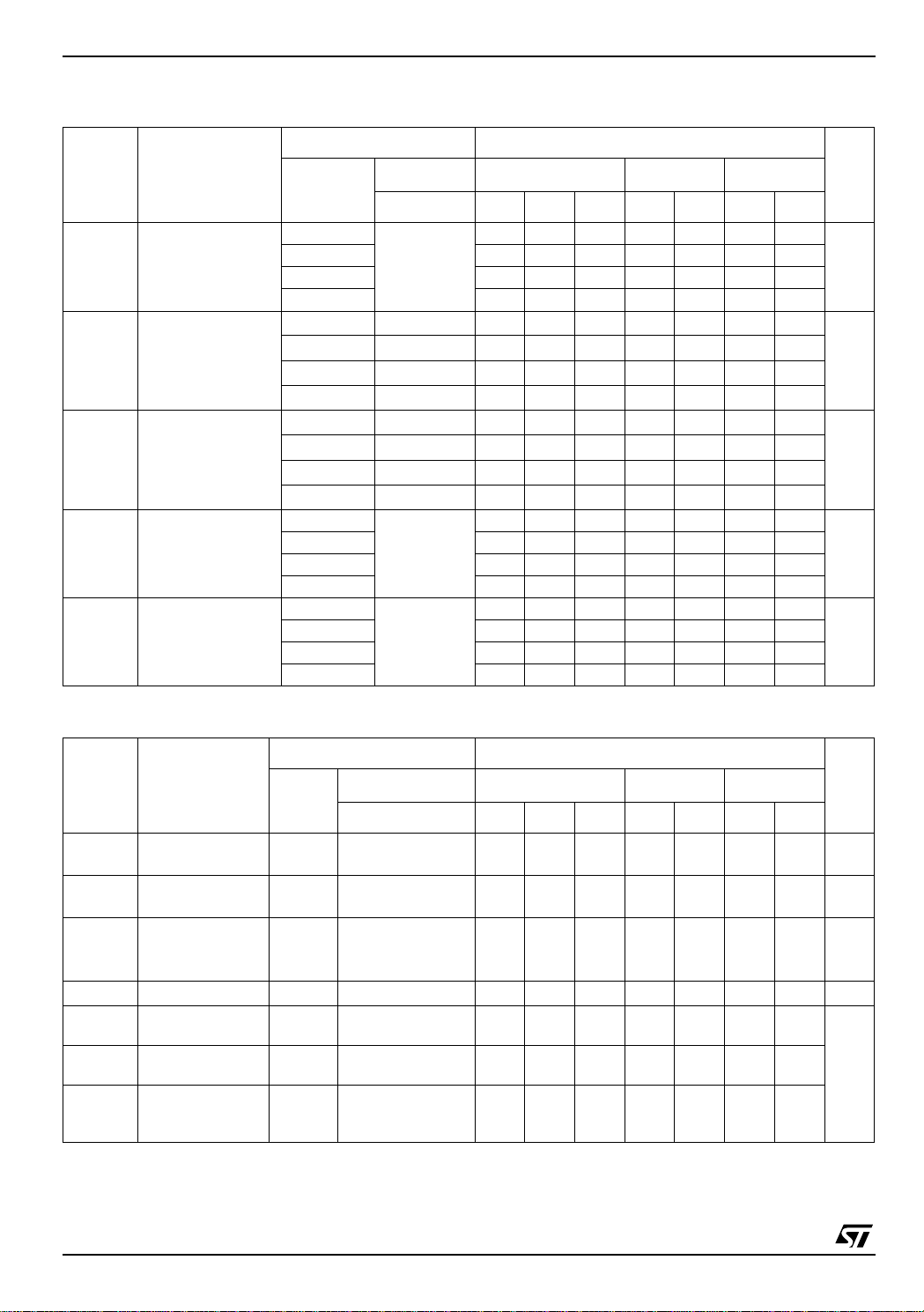
Table 6: AC Electrical Characteristics (CL=35pF,RL=50Ω, tr=tf≤ 5ns)
Test Condition Value
= 25°C
Symbol Parameter
t
PLH,tPHL
t
t
Propagation Delay 1.65-1.95
TURN-ON time 1.65-1.95 VS=0.8V
ON
TURN-OFF time 1.65-1.95 VS=0.8V
OFF
Break Before Make
Time Delay
t
D
Q Charge injection 1.65-1.95
T
V
CC
(V)
2.3-2.7 0.40
3.0-3.6 0.30
=OPEN
V
I
A
Min. Typ. Max. Min. Max. Min. Max.
3.6-4.3 0.30
2.3-2.7 V
3.0-3.6 V
3.6-4.3 V
2.3-2.7 V
3.0-3.6 V
3.6-4.3 V
1.65-1.95
2.3-2.7 2 15
3.0-3.6 2 15
3.6-4.3 2 15
2.3-2.7 200
3.0-3.6 200
3.6-4.3 200
S
S
S
S
S
S
C
=35pF
L
R
L
V
S
C
= 100pF
L
R
=1MΩ
L
V
GEN
R
GEN
=1.5V
=1.5V
=1.5V
=1.5V
=1.5V
=1.5V
=50Ω
=1.5V
=0V
=0Ω
0.45
70
30 50 60
30 50 60
30 50 60
45
25 30 40
25 30 40
25 30 40
-40 to 85°C -55 to 125°C
Unit
ns
ns
ns
ns
pC
Table 7: An alog Switch Characteristics (C
= 5pF, RL=50Ω,TA= 25°C)
L
Test Condition Value
Symbol Parameter
OIRR Off Isolation (1) 1.65-4.3 V
V
(V)
CC
=1V
S
Min. Typ. Max. Min. Max. Min. Max.
RMS
f= 100KHz
Xtalk Crosstalk 1.65-4.3 V
=1V
S
RMS
f= 100KHz
THD Total Harmonic
Distortion
2.3-4.3 R
L
V
IN
=600Ω
=2V
PP
f= 20Hz to 20kHz
BW -3dB Bandwidth 1.65-4.3 R
IN
Sn
C
D
Control Pin Input
Capacitance
Sn Port Capacitance
D Port Capacitance when
3.3
3.3
C
C
=50Ω
L
f= 1MHz 37
f= 1MHz 84
Switch is Enabled
Note 1: Off Isolation= 20Log10(VD/VS), VD= output. VS= input at off switch
= 25°C
T
A
-40 to 85°C -55 to 125°C
-64 dB
-54 dB
0.03 %
50 MHz
5
Unit
pF
4/11
Page 5

STG3680
Figure 2: ON Resi stance
Figure 3: OFF Leakage
Figure5: Bandwidth
Figure 6: Channel To Channel Crosstalk
Figure4: OFF Isolation
5/11
Page 6

STG3680
Figure7: Test Circuit
CL= 5/35pF or equivalent (includes jig and probe capacitance)
RL=50Ω or equivalent
R
T=ZOUT
Figure8: Break Before Make Time Delay
of pulse generator (typically 50Ω)
Figure 9: Charge Injection (V
6/11
GEN
=0V, R
=0Ω,RL=1MΩ,CL=100pF)
GEN
Page 7

Table 8: Turn ON, Turn OFF Delay Time
STG3680
7/11
Page 8

STG3680
QFN16 (3x3) MECHANICAL DATA
mm. inch
DIM.
MIN. TYP MAX. MIN. TYP. MAX.
A 0.80 0.90 1.00 0.032 0.035 0.039
A1 0.02 0.05 0.001 0.002
A3 0.20 0.008
b 0.18 0.25 0.30 0.007 0.010 0.012
D 3.00 0.118
D2 1.55 1.70 1.80 0.061 0.067 0.071
E 3.00 0.118
E2 1.55 1.70 1.80 0.061 0.067 0.071
e 0.50 0.020
K 0.20 0.008
L 0.30 0.40 0.50 0.012 0.016 0.020
r 0.09 0.006
E
A
E2
K
A1
e
D
b
D2
K
8/11
A3
L
r
Page 9

STG3680
Tape & Reel QFNxx/DFNxx (3x3) MECHANICAL DATA
mm. inch
DIM.
A 330 12.992
C 12.8 13.2 0.504 0.519
D20.2 0.795
N60 2.362
T 18.4 0.724
Ao 3.3 0.130
Bo 3.3 0.130
Ko 1.1 0.043
Po 4 0.157
P 8 0.315
MIN. TYP MAX. MIN. TYP. MAX.
9/11
Page 10

STG3680
Table 9: Revision History
Date Revision Description of Changes
17-May-2004 3
Characteristics at V
= 4.3 V Added on Tables 3, 4, 5, 6 and 7.
CC
10/11
Page 11

STG3680
Information furnished is believed to be accurate and reliable. However, STMicroelectronics assumes no responsibility for the
consequences of use of such inform ation nor fo r an y infring ement of p atents or o ther rights of third p arties which may r esult f rom
its use. No license is granted by implication or otherwise under any patent or patent rights of STMicroelectronics. Specifications
mentioned in this publication are subject to change without notice. This publication supersedes and replaces all information
previously supplied. STMicroelectronics products are not authorized for use as critical components in life support devices or
systems without express written approval of STMicroelectronics.
Australia - Belgium - Brazil - Canada - China - Czech Republic - Finland - France - Germany - Hong Kong - India - Israel - Italy - Japan -
Malaysia - Malta - Morocco - Singapore - Spain - Sweden - Switzerland - United Kingdom - United States.
The ST logo is a registered trademark of STMicroelectronics
All other names are the property of their respective owners
© 2004 STMicroelectronics - All Rights Reserved
STMicroelectronics GROUP OF COMPANIES
http://www.st.com
11/11
Page 12

WWW.ALLDATASHEET.COM
Copyright © Each Manufacturing Company.
All Datasheets cannot be modified without permission.
This datasheet has been download from :
www.AllDataSheet.com
100% Free DataSheet Search Site.
Free Download.
No Register.
Fast Search System.
www.AllDataSheet.com
 Loading...