

Page 1
RIVA 128™
128-BIT 3D MULTIMEDIA ACCELERATOR
™
1/77
The information in this datash eet is subject to change
42 1687 01 (SGS-THOMSON)
October 1997
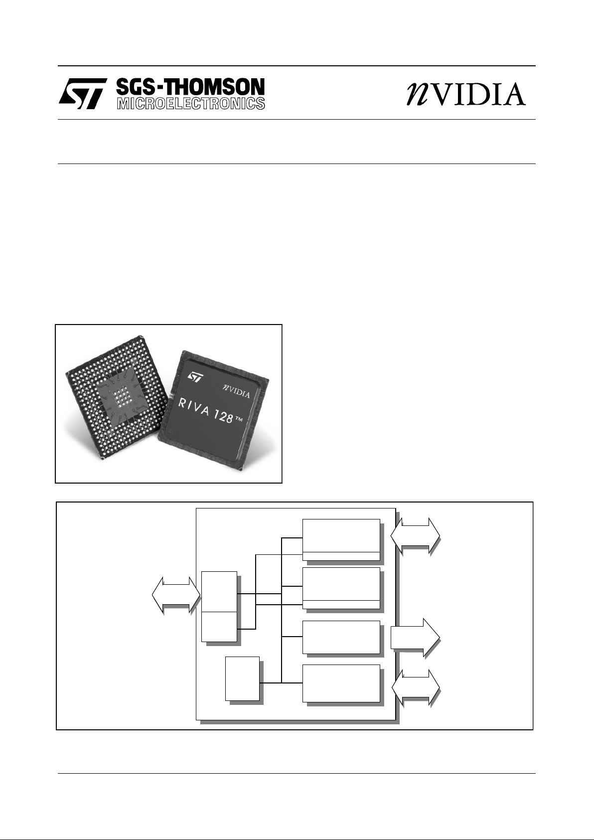
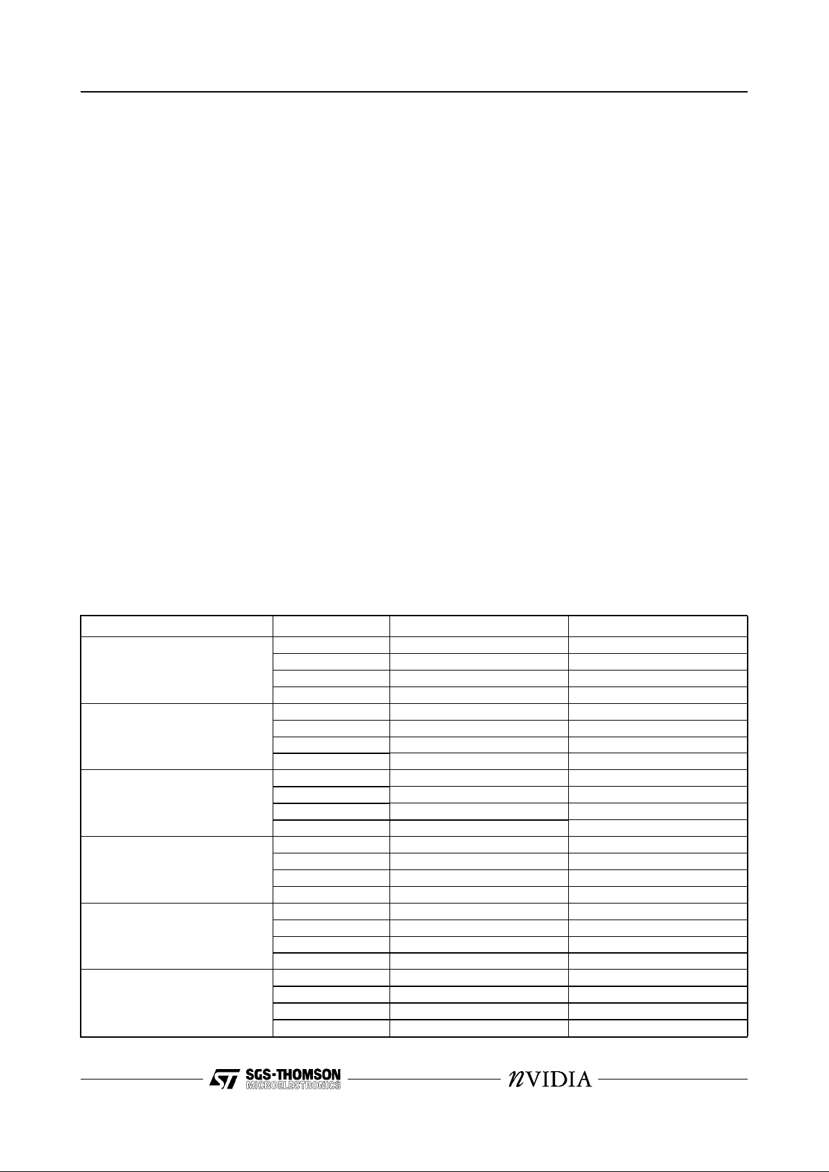
BLOCK DIAGRAM
Palette DAC
YUV - RGB,
Graphic s E ng i ne
128 bit 2D
Direct3D
SGRAM Interface
VGA
DMA Bus
Internal Bus
CCIR656
Video
PCI/AGP
128 bit
interface
Monitor/
TV
1.6 GByte/s
Internal Bus
Bandwidth
DMA Engine
Video Port
X & Y scaler
Host
Interface
FIFO/
DMA
Pusher
DMA Engine
DESCRIPTION
The RIVA 128™ is the first 128-bit 3D Multimedia
Accelerator to offer unparalleled 2D and 3D performance, meeting all the r equirements of the mainstream PC graphics market and Microsoft’s
PC’97. The RIVA 128 introduces the most advanced Direct3D™ acceleration solution and also
delivers leadership VGA, 2D and Video performance, enabling a range of applications from 3D
games through to DVD, Intercast™ and video conferencing.
KEY FEATURES
•
Fast 32-bit VGA/SVGA
•
High performance 128-bit 2D/GUI/DirectDraw
Acceleration
•
Interactive, Photorealistic Direct3D Acceleration with advanced effects
•
Massive 1.6Gbytes/s, 100MHz 128-bit wide
frame buffer interface
•
Video Acceleration for DirectDraw/DirectVideo,
MPEG-1/2 and Indeo
®
- Planar 4:2:0 and packed 4:2:2 Color Space
Conversion
- X and Y smooth up and down scaling
•
230MHz Palette-DAC supporting up to
1600x1200@75Hz
•
NTSC and PAL output with flicker-filter
•
Multi-function Video Port and serial interface
•
Bus mastering DMA 66MHz Accelerated
Graphics Port (AGP) 1.0 Interface
•
Bus mastering DMA PCI 2.1 interface
•
0.35 micron 5LM CMOS
•
300 PBGA
Page 2

RIVA 128 128-BIT 3D MULTIMEDIA ACCELERATOR
TABLE OF CONTENTS
2/77
1 REVISION HISTORY...................................................................................................................... 4
1 RIVA 128 300PBGA DEVICE PINOUT.......................................................................................... 5
2 PIN DESCRIPTIONS...................................................................................................................... 6
2.1 ACCELERATED GRAPHICS PORT (AGP) INTERFACE..................................................... 6
2.2 PCI 2.1 LOCAL BUS INTERFACE........................................................................................ 6
2.3 SGRAM FRAMEBUFFER INTERFACE................................................................................ 8
2.4 VIDEO PORT......................................................................................................................... 8
2.5 DEVICE ENABLE SIGN ALS... ... .................................................... ... ..................................... 9
2.6 DISPLAY INTERFACE.......................................................................................................... 9
2.7 VIDEO DAC AND PLL ANALOG SIGNALS.......................................................................... 9
2.8 POWER SUPPLY.................................................................................................................. 9
2.9 TEST...................................................................................................................................... 10
3 OVERVIEW OF THE RIVA 128...................................................................................................... 11
3.1 BALANCED PC SYSTEM...................................................................................................... 11
3.2 HOST INTERFACE ...............................................................................................................11
3.3 2D ACCELERATION................. .... .............................. .... ...................................................... 12
3.4 3D ENGINE..................... ............................... ... .................................................................... 12
3.5 VIDEO PROCESSOR............................................................................................................ 12
3.6 VIDEO PORT......................................................................................................................... 13
3.7 DIRECT RGB OUTPUT TO LOW COST PAL /NT SC ENC ODER........... ... ..................... ... ... 13
3.8 SUPPORT FOR STANDAR D S...... ... ................................................... .... .............................. 13
3.9 RESOLUTIONS SUPPORTED.............................................................................................. 13
3.10 CUSTOMER EVALUATION KIT ............................................................................................ 14
3.11 TURNKEY MANUFACTURING PACKAGE........................................................................... 14
4 ACCELERATED GRAPHICS PORT (AGP) INTERFACE............................................................. 15
4.1 RIVA 128 AGP INTERFACE................................................................................................. 1 6
4.2 AGP BUS TRANSACTIONS.................................................................................................. 1 6
5 PCI 2.1 LOCAL BUS INTERFACE................................................................................................. 2 2
5.1 RIVA 128 PCI INTERFACE................................................................................................... 22
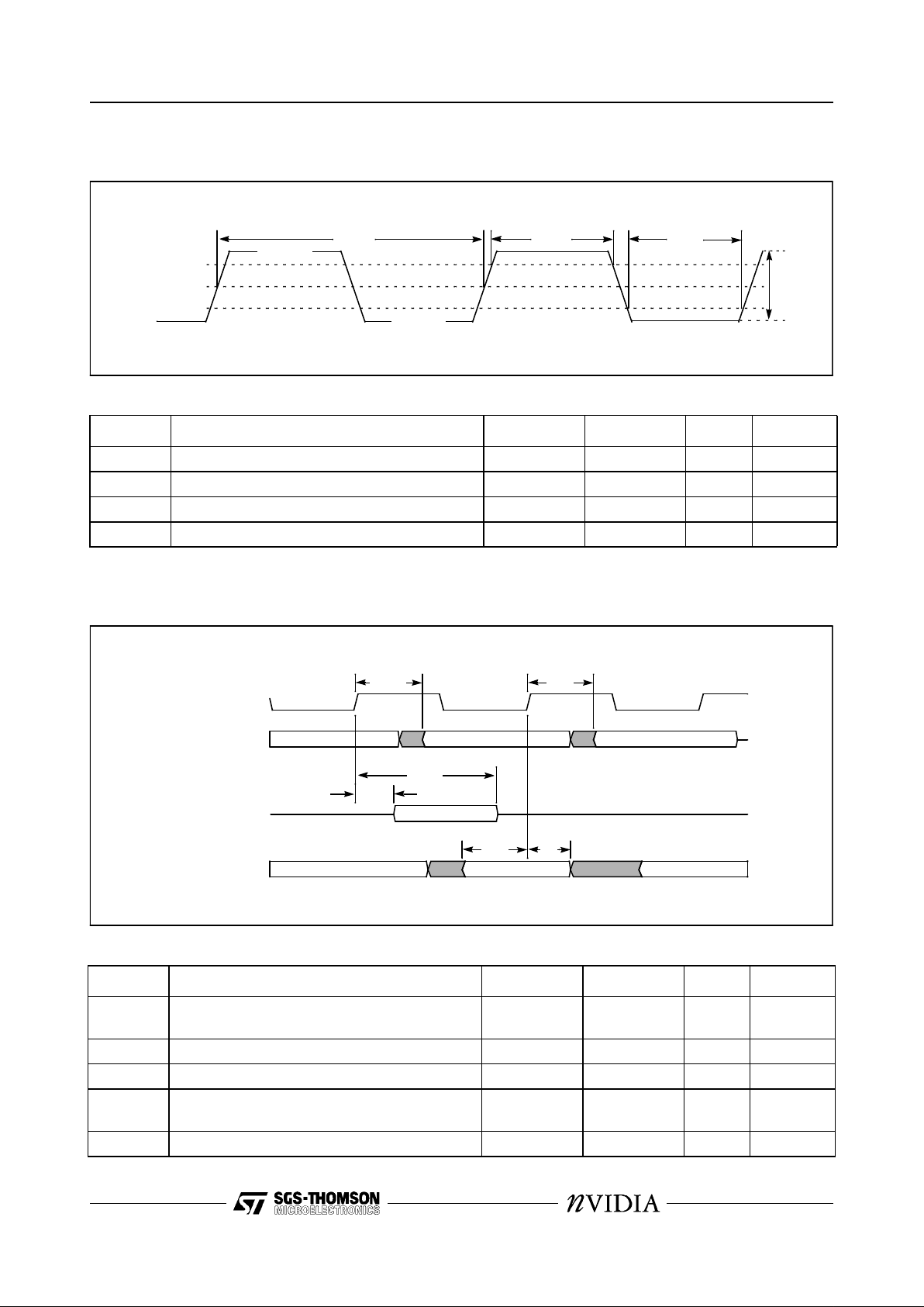
5.2 PCI TIMING SPECIFICATION............................................................................................... 23
6 SGRAM FRAMEBUFF E R INTERFA C E........... ................................................... .... ....................... 29
6.1 SGRAM INITIALIZATION...................................................................................................... 31
6.2 SGRAM MODE REGISTER.................................................................................................. 31
6.3 LAYOUT OF FRAMEBUFFER CLOCK SIGNALS................................................................ 32
6.4 SGRAM INTERFACE TIMING SPECIFICATION.................................................................. 32
7 VIDEO PLAYBACK ARCHITECTURE........................................................................................... 37
7.1 VIDEO SCALER PIPELINE ................................................................................................... 38
8 VIDEO PORT.................................................................................................................................. 40
8.1 VIDEO INTERFACE PORT FEATURES............................................................................... 40
8.2 BI-DIRECTIONAL MEDIA PORT POLLING COMMANDS USING MPC.............................. 41
8.3 TIMING DIAGRAMS..............................................................................................................42
8.4 656 MASTER MODE............................................................................................................. 46
8.5 VBI HANDLING IN THE VIDEO PORT................................................................................. 47
8.6 SCALING IN THE VIDEO PORT.............................. ... .......................................................... 47
9 BOOT ROM INTERFACE......... ................................................... .... ............................................... 48
Page 3

128-BIT 3D MULTIMEDIA ACCELERATOR RIVA 128
3/77
10 POWER-ON RESET CONFIGURATION........................................................................................ 50
11 DISPLAY INTERFACE................................................................................................................... 52
11.1 PALETTE-DAC...................................................................................................................... 52
11.2 PIXEL MODES SUPPORTED ............................................................................................... 52
11.3 HARDWARE CURSO R.......... ............................................................. .... .............................. 53
11.4 I2C INTERFACE.................................................................................................................... 54
11.5 ANALOG INTERFACE.......................................................................................................... 55
11.6 TV OUTPUT SUPPORT...................................................................... .... .............................. 56
12 IN-CIRCUIT BOARD TESTING......................................................................................................58
12.1 TEST MODES............................................................................... ... ..................................... 58
12.2 CHECKSUM TEST................................................................................................................ 58
13 ELECTRICAL SPEC IF ICA TI ONS.................................. ... ............................................................. 59
13.1 ABSOLUTE MAXIMUM RATINGS............. ................................... ........................................ 59
13.2 OPERATING CONDITIONS.................................................................................................. 59
13.3 DC SPECIFICATI ON S..... ... ............................... .... ............................................................. .. .59
13.4 ELECTRICA L SPECIFICATIONS.......................... ... ................................................... .... ...... 60
13.5 DAC CHARACTERISTICS.................................................................................................... 60
13.6 FREQUENCY SYNTHESIS CHARACTERISTICS................................................................ 61
14 PACKAGE DIMENSION SPECIFICATION.................................................................................... 62
14.1 300 PIN BALL GRID ARRAY PACKAGE.............................................................................. 62
15 REFERENCES................................................................................................................................ 63
16 ORDERING INFORMATION..........................................................................................................63
APPENDIX...................................................................................................................................... 64
A PCI CONFIGURATION REGISTERS............................................................................................. 64
A.1 REGISTER DESCRIPTIONS FOR PCI CONFIGURATION SPACE.................................... 64
Page 4
128-BIT 3D MULTIMEDIA ACCELERATORRIVA 128
4/77
1 REVISION HISTORY
Date Section, page Descripti on of change
15 Jul 97 6, page 28 Updat e of SG R AM fram ebuf fer int er face conf ig ura ti on di agrams.
28 Aug 97 13.5, page 59 Change of DAC specification from 206MHz to 230M Hz max. oper ating frequency.
29 Aug 97 6.3, page 31 Updat e t o re com mendation for connect ion of
FBCLK2
and
FBCLKB
pins.
4 Sep 97 10, page 49 Update to RAM Type Power-On Reset confi gur ation bits.
15 Sep 97 13, page 58 Temperature specificat ion TC now based on case, not ambient temperature.
15 Sep 97 13, page 58 Change to Power Supply voltage VDD specification.
17 Sep 97 1, page 5 Change to Video Port pin nam es.
17 Sep 97 2, page 6 Chang e to Vid eo Port pin descr iptions.
17 Sep 97 8, page 39 Updates to Video Port section.
18 Sep 97 11.6, page 55 Change to capacitor value in TV output implementation schematic.
18 Sep 97 13.3, page 58 Change to power dissipation specifi cat ion.
25 Sep 97 4.2, page 16 Rem oval of AGP flow control descriptio n.
25 Sep 97 11.4, page 53 Updates to Ser ial Port descrip tion.
Page 5
128-BIT 3D MULTIMEDIA ACCELERATOR RIVA 128
5/77
1 RIVA 128 300PBGA DEVICE PINOUT
NOTES
1 NIC = No Internal Connection. Do not connect to these pins.
2 VDD=3.3V
∗
Signals denoted with an asterisk are defined for future expansi on. See
Pin Descriptions
, Section 2, page 6 for details.
1234567891011121314151617181920
A
FBD[4] FBD[6] FBD[7] FBD[17] FBD[19] FBD[21] FBD[23] FBDQM[2] FBA[0] FBA[2] FBA[4] FBA[6] FBA[8] FBDQM[5] FBD[41] FBD[43] FBD[45] FBD[47] FBD[56] FBD[57]BFBD[3] FBD[5] FBD[16] FBD[18] FBD[20] FBD[22] FBDQM[0] FBA[9] FBA[1] FBA[3] FBA[5] FBA[7] FBCLK1 FBDQM[7] FBD[40] FBD[42] FBD[44] FBD[46] FBD[58] FBD[59]CFBD[1] FBD[2] FBD[28] FBD[27] FBD[26] FBD[25] FBD[15] FBD[13] FBD[11] FBD[9] FBDQM[1] FBWE# FBRAS#
FBA[10]
∗
FBDQM[4] FBD[55] FBD[54] FBD[53] FBD[60] FBD[61]
D
FBCLK0 FBD[0] FBD[29] FBD[30] VDD FBD[24] FBD[14] FBD[12] FBD[10] FBD[8] FBDQM[3] FBCAS# FBCS0 FBCS1 FBDQM[6] VDD FBD[52] FBD[51] FBD[62] FBD[63]
E
SCL FBCLK2 FBD[31] VDD NIC VDD VDD VDD
FBCKE
∗
VDD VDD VDD VDD FBD[50] FBD[39] FBD[38]
F
MP_AD[6] NIC SDA FBCLK FB VDD VDD FBD[48] FBD[49] FBD[37] FBD[36]
G
MPFRAME# MP_AD[7] MP_AD[5] MP_AD[4] MPCLAMP VDD FBD[35] FBD[34] FBD[33] FBD[32]
H
MP_AD[2] MPSTOP# MPCLK M P_AD[3] VDD NIC FBDQM[12] FBDQM[14] FBDQM[15] FBDQM[13]
J
FBDQM[8] MPDTACK# MP_AD[1] MP_AD[0] GND GND GND GND FBD[118] FBD[119] FBD[105] FBD[104]KFBDQM[9] FBD[87] FBDQM[10] FBDQM[11] GND GND GND GND FBD[116] FBD[117] FBD[107] FBD[106]
L
FBD[86] FBD[85] FBD[72] FBD[73] GND GND GND GND FBD[114] FBD[115] FBD[109] FBD[108]MFBD[84] FBD[83] FBD[74] FBD[75] GND GND GND GND FBD[112] FBD[113] FBD[111] FBD[110]NFBD[82] FBD[81] FBD[76] FBD[77] NIC NIC FBD[102] FBD[103] FBD[121] FBD[120]PFBD[80] FBD[71] FBD[78] FBD[79] VDD VDD FBD[100] FBD[101] FBD[123] FBD[122]RFBD[70] FBD[69] FBD[88] FBD[89] NIC NIC FBD[98] FBD[99] FBD[125] FBD[124]
T
FBD[68] FBD[67] FBD[90] VDD NIC HOSTVDD HO ST VDD
HOST-
CLAMP
HOSTVDD
HOST-
CLAMP
HOSTVDD
HOST-
CLAMP
VDD FBD[97] FBD[127] FBD[126]
U
FBD[66] FBD[65] FBD[92] FBD[91]
HOST-
CLAMP
XTALOUT PCIRST# AGPST[1] PCIAD[30] PCIAD[26] PCICBE# [3] PCIAD[20 ] PCIAD[16] PCITRDY# PCIPAR
HOSTVDD PCICBE#[0] FBD[96] VIDVSYNC VIDHSYNC
V
FBD[64] FBD[95] RED DACVDD VREF PCIINTA# PCIGNT# AGPPIPE# PCIAD[28] PCIAD[24] PCIAD[22] PCIAD[18] PCIFRAME# PCISTOP# PCIAD[15] PCIAD[11] PCIAD[6] PCIAD[2] TESTMODEROMCS#WFBD[93] FBD[94] BLUE COMP PLLVDD PCIREQ# AGPST[2] PCIAD[31] PCIAD[27]
AGPAD-
STB1
∗
PCIAD[21] PCIAD[17] PCIIRDY# PCICBE#[1] PC IAD[ 13] PCIAD[9] PCIAD[4] PCIAD[0] PCIAD[7] PCIAD[5]
Y
GREEN GND R SET XTALIN PCICLK AGPST[0]
PCIIDSEL/
AGPRBF#
PCIAD[29] PCIAD[25] PCIAD[23] PCIAD[19] PCICBE#[2 ]
PCI-
DEVSEL#
PCIAD[14] PCIAD[12] PCIAD[10] PCIAD[8]
AGPAD-
STB0
∗
PCIAD[3] PCIAD[1 ]
Page 6
128-BIT 3D MULTIMEDIA ACCELERATORRIVA 128
6/77
2 PIN DESCRIPTIONS
2.1 ACCELERATED GRAPHICS PORT (AGP) INTERFACE
2.2 PCI 2.1 LOCAL BUS INTERFACE
Signal I/O Description
AGPST[2:0]
I AGP status bus providing information from the arbiter to the RIVA 128 on what it may do.
AGPST[2:0]
only have meaning to the RIVA 128 when
PCIGNT#
is asserted. W hen
PCIGNT#
is de-asser t ed t hese signals have no meaning and must be ignore d.
000 Indicate s tha t previously requested low priority read or flush data is being
returned to the RIVA 128.
001 Indica te s tha t previously requested hi gh priority r ead data is being ret urned to
the RIVA 128.
010 Indica te s tha t the RIVA 128 is to provide low priority write data for a previous
enqueued wr it e com m and.
011 Indicates that the RIVA 128 is to provide high priority write data for a previous
enqueued wr it e com m and.
100 Reserved
101 Reserved
110 Reserved
111 Indicate s tha t the RIVA 128 has been given permission to sta rt a bus transac-
tion. The RIVA 128 may enqueue AGP requests by asserting
AGPP IPE#
or sta rt
a PCI transaction by asserting
PCIFRAME#. AGPST[2:0]
are always an output
from the Core Logic (AGP chipset) and an input to the RIVA 128.
AGPRBF#
O Read Buffer Full indicates when the RIVA 128 is ready to accept previously requested low
priority read data or not. When
AGPRBF#
is assert ed t he ar biter is not allowed to return
(low priority) read data to the RIVA 128. This signal should be pulled up via a 4.7KΩ resistor (although it is supposed to be pull ed up by the motherboard chipset).
AGPPIPE#
O Pipel ine d Re ad is asserted by RIVA 128 (when the current master) to indicat e a full w id th
read address is to be enqu eued by the target. The RI VA 128 enqueues one requ est each
rising clock edge while
AGPPIPE#
is assert ed. When
AGPPIPE#
is de-asserted no new
requests are enqueued across
PCIAD[31:0]. AGPPIPE#
is a sustained tri-state signal
from the RIVA 128 and is an input to the target (the core logic).
AGPADSTB0
∗,
AGPADSTB1
∗
I/O These signals are currently a “no-connect” in this revision of the RIVA 128 but may be acti-
vated to support AGP double-edge clocking in future pin compatible devices. It is recommended that thes e pins are connected directly to the AD _S TB0 and AD_STB1 pins
defined in the AGP specification.
Signal I/O Descripti on
PCICLK
I PCI clock. This si gnal pr ovides timing for all transaction s on th e PC I bus, except for
PCIRST#
and
PCIINTA#
. All PCI signals are sampl ed on the rising edge of
PCICLK
and
all timing parameters are defined with respect to this edge.
PCIRST#
I PCI reset. This signal is used to bring registers, sequencers and signals to a consistent
state. When
PCIRST#
is asserted all output signals are t r istated.
PCIAD[31:0]
I/O 32-bit multiplexed address and data bus. A bus transaction cons ists of an address phase
followed by one or more data phases.
Page 7
128-BIT 3D MULTIMEDIA ACCELERATOR RIVA 128
7/77
PCICBE[3:0]#
I/O Multiplexed bus command and byte enable signals. During t he address phase of a trans-
action
PCICBE[3:0]#
define the bus command, during the dat a phase
PCICBE[3:0]#
are
used as byte enables. The byte enables are valid for the entire data phase and determine
which byte lanes contain valid data.
PCICBE[0]#
applies to byte 0 (LSB) and
PCICBE[3]#
applies to byte 3 (MSB).
When connected to AGP these signals carry different commands than PCI when requests
are being enqueued using
AGPPIPE#
. Valid byte information is provided during AGP write
transactions.
PCICBE[3:0]#
are not used during the return of AGP read data.
PCIPAR
I/O Parity. Th is si gnal is the even parity bit generated acr oss
PCIAD[31:0]
and
PCICBE[3:0]#. PCIPAR
is stable and valid one clock after the address phase. For data
phases
PCIPAR
is stable and valid one clock after either
PCIIRDY#
is asserted on a write
transaction or
PCITRDY#
is asserted on a r ead transaction. Once
PCIPAR
is valid, it
remains valid until one clock after completion of the current data phase. The master drives
PCIPAR
for address and write data phases; the target drives
PCIPAR
for read data
phases.
PCIFRAME#
I/O Cycle frame. This signal is driven by the current master to indicate the beginning of an
access and its duration.
PCIFRAME#
is asserted to indi cat e t hat a bus transact ion is
beginning. Dat a transfers continue while
PCIFRAME#
is assert ed. When
PCIFRAME#
is
deassert ed, the transactio n is in the final data phase.
PCIIRDY#
I/O Initiator ready. This signal indicates the initiator’s (bus master’s) ability to complete the cur-
rent data phase of the tran sact ion. See extended descri pt ion for
PCITRDY#
.
When connected to AGP this signal indicates the initiator (AGP compliant master) is ready
to provide all write data for the current transaction. Once
PCIIRDY#
is asserted for a write
operation, the master is not allowed to insert wait states. The assertion of
PCIIRDY#
for
reads, indicates that the ma ste r is re ady to transfer a subsequent block of read data. The
master is never allowed to insert a wait state during the initial block of a read t rans act io n.
However, it may ins ert wa it states after ea c h bl o ck trans fers.
PCITRDY#
I/O Target rea dy. This signal indicates the tar get ’s (selecte d device’s) ability to compl et e th e
current data phase of the transaction.
PCITRDY#
is used in conjunction with
PCIIRDY#
. A data phase is completed on any clock
when both
PCITRDY#
and
PCIIRDY#
are sampled as being asser te d. During a read,
PCITRDY#
indicates that valid data is present on
PCIAD[31:0]
. During a write, it in dica tes
the target is prepared to accept data. Wait cycles are inserted until bot h
PCIIRDY#
and
PCITRDY#
are asser t ed together.
When connected to AGP this signal indicates the AGP compliant target is ready to provide
read data for the entire transact ion (when transaction can complete with in four clocks) or
is ready to transfer a (initial or subsequent) block of data, when the transfer requires more
than four clocks to complete. The target is al lowed to insert wait states af t er each block
transfers on both read and write transactions.
PCISTOP#
I/O
PCISTOP#
indicates that the current target is requesting the master to terminate the cur-
rent transaction.
PCIIDSEL
I Initializ at ion device select. This signa l is used as a chip select during configuration read
and write transacti ons.
For AGP applications note that ID S EL i s not a pin on the AGP connector. The RIVA 128
performs the device select de code internally within its host interface. It is not required to
connect the AD16 signal to the IDSEL pin as suggested in the AGP specifica tion.
PCIDEVSEL#
I/O Device select. When acting as an output
PCIDEVSEL#
indicates that the RIVA 128 has
decoded the PCI address and is claimin g the cur re nt access as the target. As an input
PCIDEVSEL#
indicates w hethe r any ot her de vice on t he bu s ha s been se l ecte d .
PCIREQ#
O Request. This signal is asserted by the RIVA 128 to indicate to the arbiter that it desires to
become master of the bus.
Signal I/O Description
Page 8
128-BIT 3D MULTIMEDIA ACCELERATORRIVA 128
8/77
2.3 SGRAM FRAMEBUFFER INTERFACE
2.4 VIDEO PORT
PCIGNT#
I Grant. This sign al i ndi cat es to the RI VA 128 that access to the bus has bee n granted and
it can now become bus master.
When connected to AGP additional information is provided on
AGPST[2:0]
indicating that
the master is the recipient of previously requested read data (high or low priority), it is to
provide write dat a (h igh or low priorit y ), for a previous ly en queued write command or has
been given permis sion to start a bus transaction (AGP or PCI).
PCIINTA#
O Interrupt reques t line. This open drain output is asserted and deasserted async hronously
to
PCICLK
.
Signal I/O Descripti on
FBD[127:0]
I/O The 128-bit SGRAM memory data bus.
FBD[31:0]
are also used to access up to 64KBytes of 8-bit ROM or Fla sh ROM, using
FBD[15:0]
as address ROMA[15 :0 ],
FBD[31:2 4]
as ROMD[7:0],
FBD[17]
as ROMWE#
and
FBD[16]
as ROMOE#.
FBA[10:0]
O Memory Address bus. Conf igu ratio n st rap pin g options are also deco ded on these signals
during PCIRST# as descri bed i n Section 10, page 49.
[FBA[10]
is reserved for future
expansion and should be pu ll ed t o
GND
via a 4.7KΩ resistor.
FBRAS#
O Memory Row Address Strobe for all memory devices.
FBCAS#
O Memory Column Address Strobe for all memory devices.
FBCS[1:0]#
O Memory Chip Select strobes for each SGRAM bank.
FBWE#
O Memory Write Enable strobe for all memory devices.
FBDQM[15:0]
O Memory Data/Output Enable strobes for each of the 16 bytes.
FBCLK0,
FBCLK1,
FBCLK2
O Memory Clock signals. Sepa rate cl ock signals
FBCLK0
and
FBCLK1
are pr ovided fo r
each bank of SGRAM for reduced clock skew and loading.
FBCLK2
is fed back to
FBCLKFB
. Details of recommended memor y cl ock layout are given in Sect ion 6.3 , pag e
31.
FBCLKFB
I Framebuffer clock feedback.
FBCLK2
is fed back to
FBCLKFB
.
FBCKE
∗ O This signal is currently a “no-connect” in this revision of the RIVA 128 but may be activated
to support the framebuffer memory clock enable for power management in future pin compatible devices. It is recommended that this pin is tied t o VD D t hr ough a 4.7KΩ pull-up
resistor.
Signal I/O Description
MP_AD[7:0]
I/O Media Port 8-bit multiplexed address and data bus or ITU- R- 656 video data bus when in
656 mode.
MPCLK
I 40MHz Me di a Por t sys tem cl ock or pixel clock when in 65 6 m ode.
MPDTACK#
I Media Port data transfer acknowledgment signal.
MPFRAME#
O Initiates Media Port transfers when ac tive, ter m inates transfers when inactive.
MPSTOP#
I Media Port control signal used by the slave to terminate transfers.
Signal I/O Description
Page 9
128-BIT 3D MULTIMEDIA ACCELERATOR RIVA 128
9/77
2.5 DEVICE ENABLE SIGNALS
2.6 DISPLAY INTERFACE
2.7 VIDEO DAC AND PLL ANALOG SIGNALS
2.8 POWER SUPPLY
Signal I/O Description
ROMCS#
O Enables reads from an external 64Kx 8 or 32Kx8 ROM or Flash ROM. Thi s signal is used
in conjunction with framebuffer data lines as described above in Section 2.3.
Signal I/O Descripti on
SDA
I/O Used for DDC2B+ monitor communica ti on and interface to video decoder devices.
SCL
I/O Used for DDC2B+ monitor communica ti on and interface to video decoder devices.
VIDVSYNC
O Vertical sync supplied to the display monitor. No buffering is required. In TV mode this sig-
nal supplies composite sync to an externa l PAL/NTSC encoder.
VIDHSYNC
O Hor izon tal sync supplied to the displ ay monito r. No buffering is required .
Signal I/O Descripti on
RED,
GREEN,
BLUE
O RGB display moni t or out puts. These are softwar e configurable to drive eith er a doubly ter -
minated or singly terminated 75Ω load.
COMP
- Externa l compensation capacitor for the video DACs. This pin should be connected to
DACVDD
via the compensat io n capacitor, see Figure 58, page 54 .
RSET
- A precision resis to r placed between this pin and GND sets the full-scal e video DAC current, see Figure 58, page 54.
VREF
- A capacitor sho uld be placed between thi s pin and GND as shown in Figure 58, page 54.
XTALIN
I A series resonant crystal is connected between these two points to provide the reference
clock for the internal MCLK and VCLK clock synthesizers, see Figu re 58 and Table 16,
page 54. Alternately, an external L V TTL clock oscillator output may be driven into
XTA-
LOUT
, connecting
XTALIN
to GND. For designs supporting TV-out,
XTALOUT
should be
driven by a reference clock as described in Se ct ion 11.6, page 55.
XTALOUT
O
Signal I/O Descripti on
DACVDD
P Analog power supply for the video DACs.
PLLVDD
P Analog power supply for all clock synthesizers.
VDD
P Digital power supply.
GND
P Ground.
MPCLAMP
P
MPCLAMP
is connected to +5V to protect the 3.3V RIVA 128 from external devices which
will potentially dr ive 5V signal levels onto the Video Port in put pin s.
HOSTVDD
P
HOSTVDD
is connected to the Vddq 3. 3 pins on the AGP connector. This is the supply
voltage for the I/O buffers and is isolated from the core VD D. On AGP designs these pins
are also connect ed t o the
HOSTCLAMP
pins. On PCI designs they are con nected to the
3.3V supply.
HOSTCLAMP
P
HOSTCLAMP
is the supply signalling rail protection for the host interface. In AGP designs
these signals are con nected to Vddq 3.3. For PCI desig ns th ey are co nnected to the I/O
power pins (V
(I/O)
).
Page 10
128-BIT 3D MULTIMEDIA ACCELERATORRIVA 128
10/77
2.9 TEST
Signal I/O Description
TESTMODE
I For designs which wi ll be t est ed in -circuit, this pin sho uld be connected to GND throu gh a
10KΩ pull-down resi sto r, otherwise this pin should be conne cte d directly to GND. When
TESTMODE
is asser te d,
MP_AD[3:0]
are reassigned as
TESTCTL[ 3:0]
respectively.
Information on in -c ircuit test is given in Section 12, page 57.
Page 11

128-BIT 3D MULTIMEDIA ACCELERATOR RIVA 128
11/77
3 OVERVIEW OF THE RIVA 128
The RIVA 128 is the first 128-bit 3D Mu ltimedia
Accelerator to offer unparalleled 2D and 3D performance, meeting all the requirements of the mainstream PC graphics market and Microsoft’s
PC’97. The RIVA 128 introduces the most advanced Direct3D™ accelera tion solution and al so
delivers leadership VGA, 2D and Video performance, enabling a range of applications from 3D
games through to DVD, Intercast™ and video conferencing.
3.1 BALANCED PC SYSTEM
The RIVA 128 is designed to leverage existing PC
system resources such as system memory, high
bandwidth internal buses and bus master capabilities. The synergy between the RIVA 128 graphics
pipeline architecture and that of the current generation PCI and next generation AGP platforms, defines ground breaking performance levels at the
cost point currently required for mainstream PC
graphics solutions.
Execute versus DMA models
The RIVA 128 is architected to optimize PC system resources in a manner consistent with the
AGP “Execute” model
. In this model texture map
data for 3D applications is stored in system memory and individual texels are accessed as needed
by the graphics pipeline. This is a significant enhancement over the DMA model where entire texture maps are transferred into off-screen framebuffer memory.
The advantages of the Execute versus the DMA
model are:
•
Improved system performance since only the
required texels and not the e ntire texture ma p,
cross the bus.
•
Substantial cost savings since all the framebuffer is usable for the displayed screen and Z buffer and no part of it i s required to b e dedicated
to texture storage or texture caching.
•
There is no software overhead in the Direct3D
driver to manage texture caching between application memory and the framebuffer.
To extend the advantages of the Execute model,
the RIVA 128’s proprietary tex ture cache and virtual DMA bus master design overcomes the bandwidth limitation of PCI, by sustaining a hi gh texel
throughput with minimum bus utilization. The host
interface supports burst transactions up to 66MHz
and provides over 200MBytes/s on AGP. AGP ac-
cesses offer other performance enhancements
since they are from non-cacheable memory (no
snoop) and can be low priority to prevent processor stalls, or high priority to prevent graphics engine stalls.
Building a balanced system
RIVA 128 is architected to provide the level of 3D
graphics performance and quality available in top
arcade platforms. To provide comparable scene
complexity in the 1997 time-frame, processors will
have to achieve new levels of floating point performance. Profiles have shown that 1997 mainstream CPUs will be ab le to transform ove r 1 million lit, meshed triangles/s at 50% utilization using
Direct3D. This represents an order of magnitude
performance increase over anything attainable in
1996 PC games.
To build a balanced system the gr aphics pipeline
must match the CPU’s performance. It must be capable of rendering at least 1 million polygons/s in
order to avoid CPU stalls. Factors affecting this
system balance include:
•
Direct3D compatibility. Minimizing the differences between the hardware interface and the
Direct3D data structures.
•
Triangle setup. Minimizing the number of format conversions and delta calculations done by
the CPU.
•
Display-list processing. Avoiding CPU stalls by
allowing the graphics pipeline to execute independently of the CPU.
•
Vertex caching. Avoids saturating the host interface with repeated vertices, lowering the traffic on the bus and reducing system memory collisions.
•
Host interface performance.
3.2 HOST INTERFACE
The host interface boosts communication between
the host CPU and the RIVA 128. The optimized interface performs burst DMA bus mastering for efficient and fast data transfer.
•
32-bit PCI version 2.1 or AGP version 1.0
•
Burst DMA Master and target
•
33MHz PCI clock rate or 66MHz AGP clock rate
•
Supports over 100MBytes/s with 33MHz PCI
and over 200MBytes/s on 66MHz AGP
•
Implements read buffer posting on AGP
•
Fully supports the “Execute” model on both PCI
and AGP
Page 12

128-BIT 3D MULTIMEDIA ACCELERATORRIVA 128
12/77
3.3 2D ACCELERATION
The RIVA 128's 2 D rendering engine delivers in-
dustry-leading Windows acceleration performance:
•
100MHz 128-bit graphics engine optimized for
single cycle operation into the 128-bit SGRAM
interface supporting up to 1.6GBytes/s
•
Acceleration functions optimized for minimal
software overhead on key GDI calls
•
Extensive support for DirectDraw in
Windows95 including optimized Direct Framebuffer (DFB) access with Write-combining
•
Accelerated primitives including BLT, transparent BLT, stretchBLT, points, lins, lines,
polylines, polygons, fills, patterns, arbitrary
rectangular clipping and improved text rendering
•
Pipeline optimized for multiple color depth s including 8, 15, 24, and 30 bits per pixel
•
DMA Pusher allows the 2D graphics pipeline to
load rendering methods optimizing RIVA 12 8/
host multi-tasking
•
Execution of all 256 Raster Operations (as defined by Microsoft Windows) at 8, 15, 24 and
30-bit color depths
•
15-bit hardware color cursor
•
Hardware color ditheri ng
•
Multi buffering (Double, Triple, Quad buffering)
for smooth animation
3.4 3D ENGINE
Triangle setup engine
•
Setup hardware optimized for Microsoft’s
Direct3D API
•
5Gflop floating point geometry processor
•
Slope and setup calculations
•
Accepts IEEE Single Precision format used in
Direct3D
•
Efficient vertex caching
Rendering engine
The RIVA 128 Multimedia Accelerator integrates
an orthodox 3D rendering pipeline and triangle
setup function which not only fully utilizes the capabilities of the Accelerated Graphics Port, but
also supports advanced texture mapped 3D o ver
the PCI bus. The RIVA 128 3D pipeline offers to
Direct3D or similar APIs advanced triangle rendering capabilities:
•
Rendering pipeline optimized for Microsoft’s
Direct3D
API
•
Perspective correct true-color Gouraud lighting
and texture mapping
•
Full 32-bit RGBA texture filter and Gouraud
lighting pixel data path
•
Alpha blending for translucency and transparency
•
Sub-pixel accurate texture mapping
•
Internal pixel path: up to 24bits, alpha: up to 8
bits
•
Texture magnification filtering wit h high quality
bilinear filtering without performance degr adation
•
Texture minification filtering with MIP mapping
without performance degradation
•
LOD MIP-mapping: filter shape is dynamically
adjusted based on surface orientation
•
Texture sizes from 4 to 2048 texels in either U
or V
•
Textures can be looped and paged in real time
for texture animation
•
Perspective correct per-pixel fog for atmospheric effects
•
Perspective correct specular highlights
•
Multi buffering (Double, Triple, Quad buffering)
for smooth 3D animation
•
Multipass rendering for environmental mapping
and advanced texturing
3.5 VIDEO PROCESSOR
The RIVA 128 Palette-DAC pipeline accelerates
full-motion video playback, sustaining 30 frames
per second while retaining the highest quality color
resolution, implementing true bilinear filtering for
scaled video, and compensating for filtering losses
using edge enhancement algorithms.
•
Advanced support for DirectDraw (DirectVideo)
in Windows 95
•
Back-end hardware video scaling for video conferencing and playback
•
Hardware color space conversion (YUV 4:2:2
and 4:2:0)
•
Multi-tap X and Y filtering for superior image
quality
•
Optional edge enhancement to retain video
sharpness
•
Support for scaled field interframing for reduced
motion artifacts and reduced storage
Page 13
128-BIT 3D MULTIMEDIA ACCELERATOR RIVA 128
13/77
•
Per-pixel color keying
•
Multiple video windows with hardware color
space conversion and filtering
•
Planar YUV12 (4:2:0) to/from packed (4:2:2)
conversion for software MPEG acceleration
and H.261 video conferencing applications
•
Accelerated playback of industry standard codecs including MPEG-1/2, Indeo, Cinepak
3.6 VIDEO PORT
The RIVA 128 Multimedia Accelerator provides
connectivity for video input devices such as Philips
SAA7111A, ITT 3225 and Samsung KS0127
through an ITU-R-656 video input bus to DVD and
MPEG2 decoders through bidirectional media port
functionality.
•
Supported through VPE extensions to
DirectDraw
•
Supports filtered down-scaling and decimation
•
Supports real time video capture via Bus Mastering DMA
•
Serial interface for decoder control
3.7 DIRECT RGB OUTPUT TO LOW COST
PAL/NTSC ENCODER
The RIVA 128 has also been designed to interface
to a standard PAL or NTSC television via a low
cost TV encoder chip. In PAL or NTSC display
modes the interlaced output is internally flicker-filtered and CCIR/EIA compliant timing reference
signals are generated.
3.8 SUPPORT FOR STANDARDS
•
Multimedia support for MS-DOS, Windows
3.11, Windows 95, and Windows NT
•
Acceleration for Windows 95 Direct APIs including Direct3D, DirectDraw and DirectVideo
•
VGA and SVGA: The RIVA 128 has an i ndustry
standard 32-bit VGA core and BIOS support. In
PCI configuration space the VGA can be enabled and disabled independently of the GUI.
•
Glue-less Accelerated Graphics Port (AGP 1.0)
or PCI 2.1 bus interface
•
ITU/CCIR-656 compatible video port
•
VESA DDC2B+, DPMS, VBE 2.0 supported
3.9 RESOLUTIONS SUPPORTED
Resolution BPP 2MByte 4MByte (128-bit)
640x480
4 120Hz 120Hz
8 120Hz 120Hz
16 120Hz 120Hz
32 120Hz 120Hz
800x600
4 120Hz 120Hz
8 120Hz 120Hz
16 120Hz 120Hz
32 120Hz 120Hz
1024x768
4 120Hz 120Hz
8 120Hz 120Hz
16 120Hz 120Hz
32 - 120Hz
1152x864
4 120Hz 120Hz
8 120Hz 120Hz
16 120Hz 120Hz
32 - 100Hz
1280x1024
4 100Hz 100Hz
8 100Hz 100Hz
16 - 100Hz
32 - -
1600x1200
4 75Hz 75Hz
8 75Hz 75Hz
16 - 75Hz
32 - -
Page 14

128-BIT 3D MULTIMEDIA ACCELERATORRIVA 128
14/77
3.10 CUSTOMER EVALUATION KIT
A Customer Evaluation Kit (CEK) is available for
evaluating the RIVA 128. The CEK includes a PCI
or AGP adapter card designed to support the RIVA
128 feature set, an evaluation CD-ROM containing a fast-installation application, extensive device
drivers and programs demonstrating the RIVA 128
features and performance.
This CEK includes:
•
RIVA 128 evaluation board and CD-ROM
•
QuickStart install/user guide
•
OS drivers and files
- Windows 3.11
- Windows 95 Direct X/3D
- Windows NT 3.5
- Windows NT 4.0
•
Demonstration files and Game demos
•
Benchmark programs and files
3.11 TURNKEY MANUFACTURING PACKAGE
A Turnkey Manufacturing Package (TMP) is avail-
able to support OEM designs and development
through to production. It delivers a complete manufacturable hardware and software solution that
allows an OEM to rapidly design and bring to vol ume an RIVA 128-based product.
This TMP includes:
•
CD-ROM
- RIVA 128 Datasheet and Application Notes
- OrCAD™ schematic capture and PADS™
layout design information
- Quick Start install/user guide/release notes
- BIOS Modification program, BIOS binaries
and utilities
- Bring-up and OEM Production Diagnostics
- Software and Utilities
•
OS drivers and files
- Windows 3.11
- Windows 95 Direct X/3D
- Windows NT 3.5
- Windows NT 4.0
•
FCC/CE Certification Package
•
Content developer and WWW information
•
Partner solutions
•
Access to our password-protected web site for
upgrade files and release notes.
Page 15
128-BIT 3D MULTIMEDIA ACCELERATOR RIVA 128
15/77
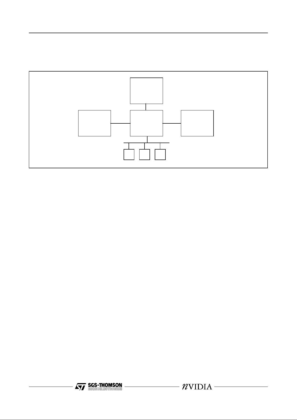
4 ACCELERATED GRAPHICS PORT (AGP) INTERFACE
The Accelerated Graphics Port (AGP) is a high performance, component level interconnect targeted at 3D
graphical display applications and based on performance enhancements to the PCI local bus.
Figure 1.
System block diagram showing relationship between AGP and PCI buses
Background to AGP
Although 3D graphics acceleration is becoming a
standard feature of multimedia PC pl atforms, 3D
rendering generally has a voracious appetite for
memory bandwidth. Consequently there is upward
pressure on the PC’s memory requirement leading
to higher bill of material costs. These trends will increase, requiring high speed access to larger
amounts of memory. The primary motivation for
AGP therefore was to contain these costs whilst
enabling performance improvements.
By providing significant bandwidth improvement
between the graphics accelerator and system
memory, some of the 3D rendering data structures
can be shifted into main memory, thus relieving
the pressure to increase the cost of the local
graphics memory.
Texture data are the first structures targeted for
shifting to system memory for four reasons:
1 Textures are generally read only, and therefore
do not have special access ordering or coherency problems.
2 Shifting textures balances the bandwidth load
between system memory and local graphics
memory, since a well cached host processor
has much lower memory bandwidth requirements than a 3D rendering engine. Texture access comprises perhaps the largest single component of rendering memory bandwi dth (compared with rendering, display and Z buffers), so
avoiding loading or caching textures in graphics
local memory saves not only this component of
local memory bandwidth, but also the bandwidth necessary to load the texture store in the
first place. Furthermore, this data must pass
through main memory anyway as it is loaded
from a mass store device.
3 Texture size is dependent upon application
quality rather than on display resolution, and
therefore subject to the greatest pressure for
growth.
4 Texture data is not persistent; it resides in
memory only for the duration of the application,
so any system memory spent on texture storage can be returned to the f ree memory heap
when the application finishes (unlike display
buffers which remain in use).
Other data structures can be moved to main memory but the biggest gai n results from moving texture data.
Relationship of AGP to PCI
AGP is a superset of the 66MHz PCI Specification
(Revision 2.1) with performance enhancements
optimized for high performance 3D graphics applications.
The PCI Specification is unmodified by AGP and
‘reserved’ PCI fields, encodings and pins, etc. are
not used.
AGP does not replace the need for the PCI bus in
the system and the two are physically, logically,
and electrically independent. As shown in Figure 1
AGP chipsetRIVA 128
System
memory
CPU
I/O I/O I/O
PCI
AGP
Page 16
128-BIT 3D MULTIMEDIA ACCELERATORRIVA 128
16/77
the AGP bridge chip and RIVA 128 are the only
devices on the AGP bus - all other I/O devices remain on the PCI bus.
The add-in slot defined for AGP uses a new connector body (for electrical signaling reasons)
which is not compatible with the PCI connector;
PCI and AGP boards are not mechanically interchangeable.
AGP accesses differ from PCI in that they are
pipelined. This compares with serialized PCI
transactions, where the address, wait and data
phases need to complete before the next transaction starts. AGP transactions can only access system memory - not other PCI devices or CPU. Bus
mastering accesses can be either PCI or AGPstyle.
Full details of AGP are given in the
Accelerated
Graphics Port Interface Specification
[3] published
by Intel Corporation.
4.1 RIVA 128 AGP INTERFACE
The RIVA 128 glueless interface to AGP 1.0 is shown in Figure 2.
Figure 2.
AGP interface pin connections
4.2 AGP BUS TRANSACTIONS
AGP bus commands supported
The following AGP bus c ommands are s upported
by the RIVA 128:
- Read
- Read (hi-priority)
PCI transactions on the AGP bus
PCI transactions can be interleaved with AGP
transactions including between pipelined AGP
data transfers. A basic PCI transaction on the AGP
interface is shown in Figure 3. If the PCI target is
a non AGP compliant master, it will not see
AGPST[2:0]
and the transaction appears to be on
a PCI bus. For AGP aware bus masters,
AGPST[2:0]
indicate that permission to use the interface has been granted to initiate a request and
not to move AGP data.
AGP bus
PCICBE[3:0]#
PCIAD[31:0]
AGPPIPE#
32
4
PCIDEVSEL#
PCIIRDY#
PCITRDY#
PCISTOP#
PCIIDSEL
PCIREQ#
PCIGNT#
PCICLK
PCIRST#
PCIPAR
PCIINTA#
RIVA 128
AGPST[2:0]#
3
AGPRBF#
Page 17

128-BIT 3D MULTIMEDIA ACCELERATOR RIVA 128
17/77
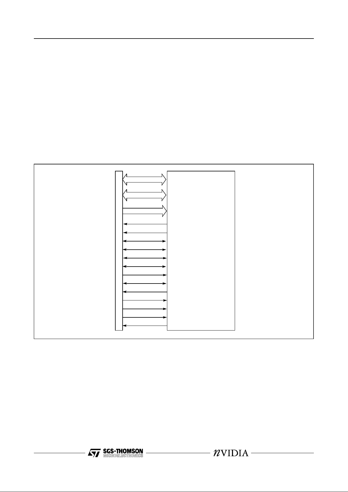
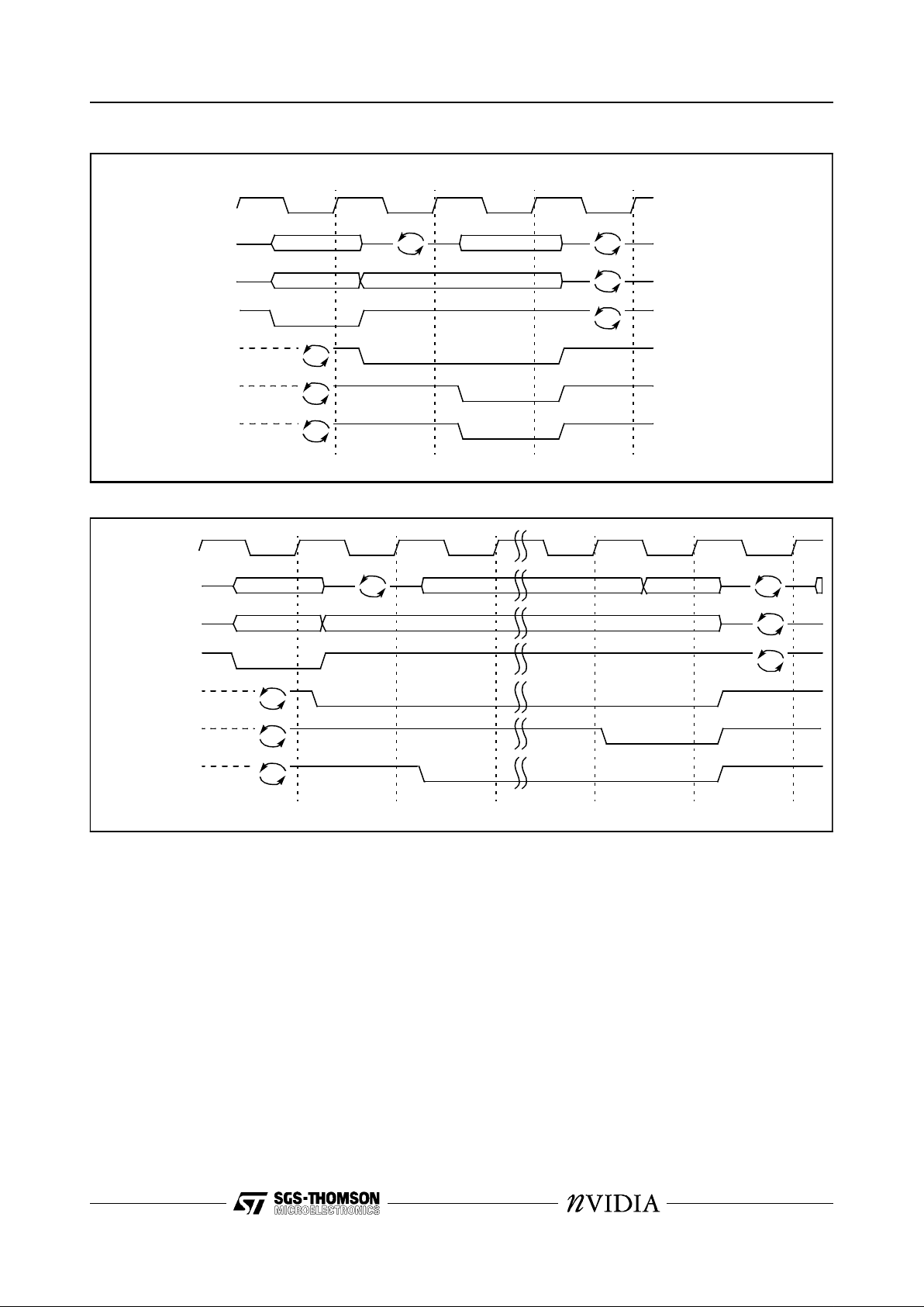
Figure 3.
Basic PCI transaction on AGP
An example of a PCI transaction occurring between an AGP command cycle and return of da ta is shown
in Figure 4. This shows the sm allest number of cycles during which an AGP request can be enqueued, a
PCI transaction performed and AGP read data returned.
Figure 4.
PCI transaction occurring between AGP request and data
bus cmd
data_pciaddress
BE[3:0]#
111 111 xxx xxx xxxxxx
PCICLK
PCIFRAME#
PCIAD[31:0]
PCICBE[3:0]#
PCIIRDY#
PCITRDY#
PCIDEVSEL#
PCIREQ#
PCIGNT#
AGPST[2:0]
134562
A9
111 xxx 111 111 xxx111
address data D7 +1
C9 pci_cmd BE 0000 000
xxx 00x xxx xxx
PCICLK
AGPPIPE#
PCIFRAME#
PCIAD[31:0]
PCICBE#
PCIIRDY#
PCITRDY#
PCIDEVSEL#
PCIAGPRBF#
PCIREQ#
PCIGNT#
AGPST[2:0]
12345678910
Page 18

128-BIT 3D MULTIMEDIA ACCELERATORRIVA 128
18/77
Figure 5.
Basic AGP pipeline concept
Pipeline operation
Memory access pipelining provides the main performance enhancement of AGP over PCI. AGP
pipelined bus transactions share most of the PCI
signal set, and are interleaved with PCI transactions on the bus.
The RIVA 128 supports AGP pipelined reads with
a 4-deep queue of outstanding read requests.
Pipelined reads are primarily used by the RIVA
128 for cache filling, the cache size being optimized for AGP bursts. Depending on the AGP
bridge, a bandwidth of up to 248MByte/s is achievable for 128-byte pipelined reads. This compares
with around 100MByte/s for 128-byte 33MHz PCI
reads. Another feature of AGP is that for smal ler
sized reads the bandwidth is not significantly reduced. Whereas 16-byte reads on PCI trans fer at
around 33MByte/s, on AGP around 175MByte/s is
achievable. The RIVA 128 actually requests reads
greater than 64 bytes in multiples of 32-byte transactions.
The pipe depth can be maintained by the AGP bus
master (RIVA 128) intervening in a pipelined transfer to insert new requests between data replies.
This bus sequencing is illustrated in Figure 5.
When the bus is in an idle conditio n, the pipe can
be started by inserting one or more AGP access
requests consecutively. Once the data reply to
those accesses starts, that stream can be br oken
(or intervened) by the bus master (RIVA 128) inserting one or more additional AGP access requests or inserting a PCI transaction. This intervention is accomplished with the bus ownership
signals,
PCIREQ#
and
PCIGNT#
.
The RIVA 128 implements both high and low priority reads depending of the status of the rendering
engine. If the pipeline is likely to stall due to system memory read latency, a high priority read request is posted.
Address Transactions
The RIVA 128 requests permission from the
bridge to use
PCIAD[31:0]
to initiate either an
AGP request or a PCI transaction by asserting
PCIREQ#
. The arbiter grants permission by as-
serting
PCIGNT#
with
AGPST[2:0]
equal to ‘111’
(referred to as START). When the RIVA 128 receives START it must start the bus operation within two clocks of the bus becoming available. F or
example, when the bus is in an idle condition when
START is received, the RIVA 128 must initiate the
bus transaction on the next clock and the one following.
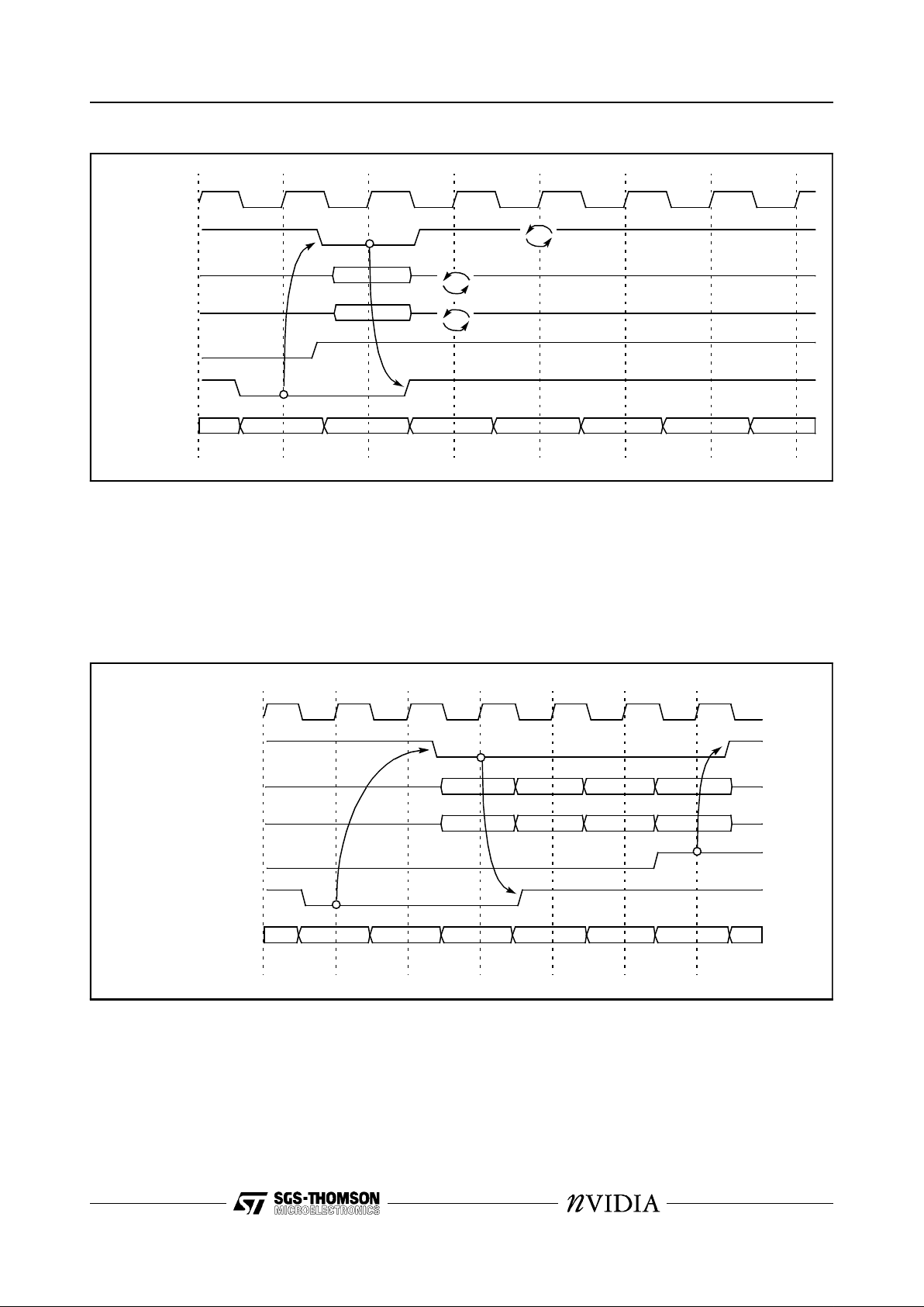
Figure 6 shows a single address being enqueued
by the RIVA 128. Sometime before clock 1, the
RIVA 128 asserts
PCIREQ#
to gain permission to
use
PCIAD[31:0]
. The arbiter grants permission
by indicating START on clock 2. A new request
(address, command and length) are enqueued on
each clock in which
AGPPIPE#
is asserted. The
address of the request to be enqueued is presented on
PCIAD[31:3]
, the length on
PCIAD[2:0]
and
the command on
PCICBE [3:0] #
. In Figure 6 only
a single address is enqueued since
AGPPIPE#
is
just asserted for a single clock. The RIVA 128 indicates that the current address is the last it intends to enqueue when
AGPPIPE#
is asserted
and
PCIREQ#
is deasserted (occurring on clock
3). Once the arbiter detects the assertion of
AGP-
PIPE#
or
PCIFRAME#
it deasserts
PCIGNT#
on
clock 4.
Bus Idle
Pipelined
data
transfer
Intervene
cycles
Pipelined AGP re quests
A1 A2
Data-1 Data-2
A3
PCI transaction
A
Data
Data-3
Page 19
128-BIT 3D MULTIMEDIA ACCELERATOR RIVA 128
19/77
Figure 6.
Single address - no delay by master
Figure 7 shows the RIVA 128 enqueui ng 4 requests, whe re the first r equest is delayed by the maximum
2 cycles allowed. START is indicated on clock 2, but the RIVA 128 does not assert
AGPPIPE#
until clock
4. Note that
PCIREQ#
remains asserted on clock 6 to indicate that the current request is not the last one.
When
PCIREQ#
is deasserted on clock 7 with
AGPPIPE#
still asserted this indicates that the current ad-
dress is the last one to be enqueued during this transaction.
AGPPIPE#
must be deasserted on the next
clock when
PCIREQ#
is sampled as deasserted. If the RIVA 128 wants to enqueue more requests during
this bus operation, it continues asserting
AGPPIPE#
until all of its requests are enqueued or until it has
filled all the available request slots provided by the target.
Figure 7.
Multiple addresses enqueued, maximum delay by RIVA 128
C1
A1
111 111 xxx xxx xxxxxx xxx xxx
PCICLK
AGPPIPE#
PCIAD[31:0]
PCICBE[3:0]#
PCIREQ#
PCIGNT#
AGPST[2:0]
12345678
A1
111 111 111 xxx xxxxxx xxx xxx
A2 A3 A4
C1 C2 C3 C4
PCICLK
AGPPIPE#
PCIAD[31:0]
PCICBE#
PCIREQ#
PCIGNT#
AGPST[2:0]
1234567
Page 20
128-BIT 3D MULTIMEDIA ACCELERATORRIVA 128
20/77
AGP timing specification
Figure 8.
AGP clock specification
Table 1.
AGP clock timing parameters
NOTES
1 This rise and fall time is measured across the minimum peak- to- peak ra nge as shown in Figure 8.
Figure 9.
AGP timing diagram
Table 2.
AGP timing parameters
Symbol Parameter Min. Max. Unit Notes
t
CYC
PCICLK
peri od 15 30 ns
t
HIGH
PCICLK
high ti me 6 ns
t
LOW
PCICLK
low time 6 ns
PCICLK
slew rate 1.5 4 V/ns 1
Symbol Parameter Min. Max. Unit Notes
t
VAL
AGPCLK
to signal valid delay (da ta and control
signals)
211ns
t
ON
Float to active delay 2 ns
t
OFF
Active to float delay 28 ns
t
SU
Input set u p time to
AGPCLK
(data and contro l
signals)
7ns
t
H
Input hold time from
AGPCLK
0ns
t
CYC
t
HIGH
t
LOW
PCICLK
0.3VDD
0.4VDD
0.5VDD
0.2VDD
0.6VDD
2V p-to-p
(minimum)
t
VAL
t
VAL
t
ON
t
OFF
t
SU
t
H
data1 data2
data1 data2
AGPCLK
Output delay
Tri-state outpu t
Input
Page 21
128-BIT 3D MULTIMEDIA ACCELERATOR RIVA 128
21/77
5 PCI 2.1 LOCAL BUS INTERFACE
5.1 RIVA 128 PCI INTERFACE
The RIVA 128 supports a glueless interface to PCI 2.1 with both master and slave capabilities. The host
interface is fully compliant with the 32-bit PCI 2.1 specification.
The Multimedia Accelerator supports PC I bus operation up to 33MHz with z ero-wait s tate capability and
full bus mastering capability handling burst reads and burst writes.
Figure 10.
PCI interface pin connections
Table 3.
PCI bus commands supported by the RIVA 128
Bus master Bus slave
Memory read and write Memory read and write
Memory read line I/O read and wr it e
Memory read multiple Configuration read and write
Memory read line
Memory read multiple
Memory write invalidate
PCI bus
PCICBE[3:0]#
PCIAD[31:0]
PCIFRAME#
32
4
PCIDEVSEL#
PCIIRDY#
PCITRDY#
PCISTOP#
PCIIDSEL
PCIREQ#
PCIGNT#
PCICLK
PCIRST#
PCIPAR
PCIINTA#
RIVA 128
Page 22
128-BIT 3D MULTIMEDIA ACCELERATORRIVA 128
22/77
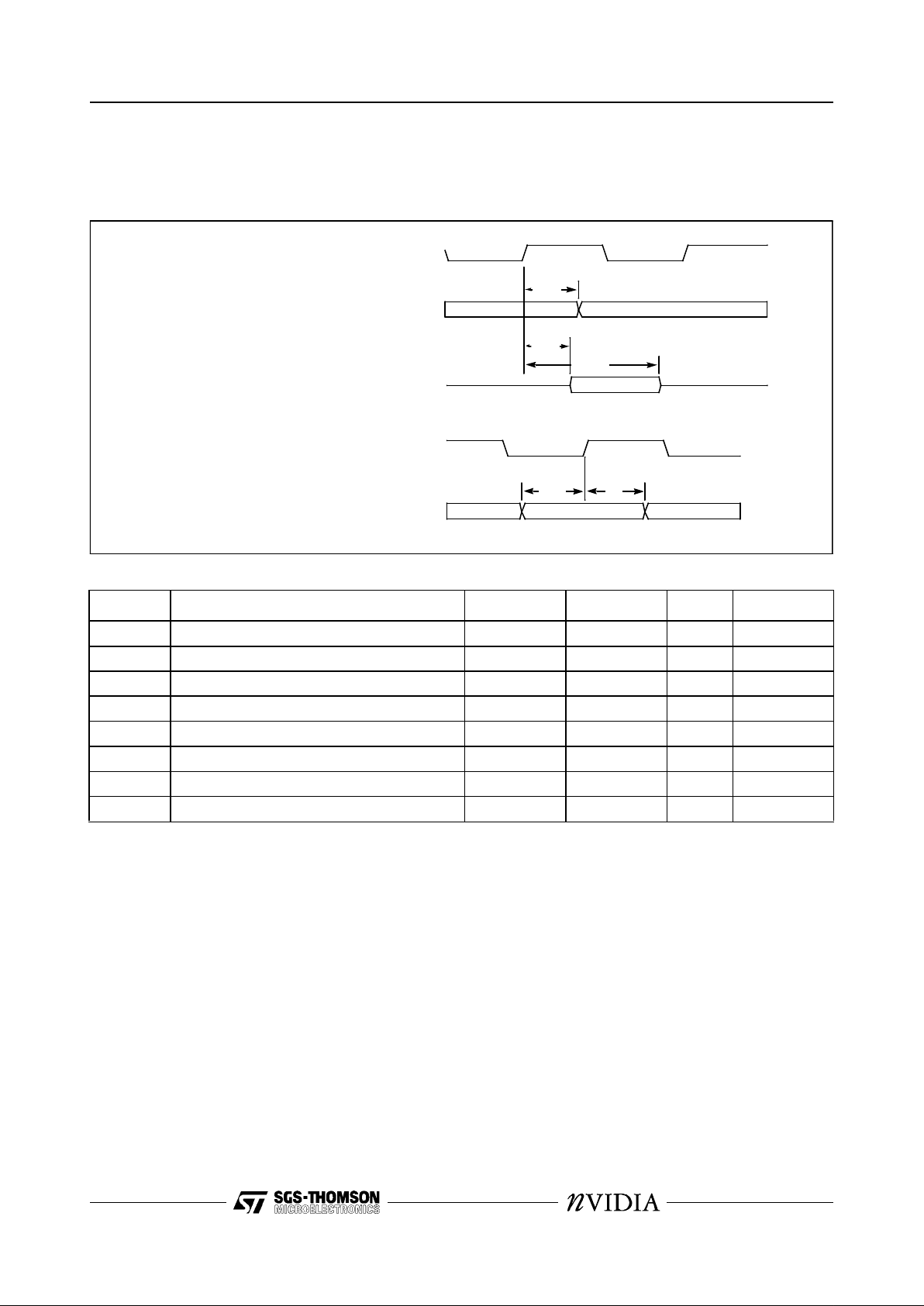
5.2 PCI TIMING SPECIFICATION
The timing specification of the PCI interface takes the form of generic setup, hold and delay times of tran-
sitions to and from the rising edge of
PCICLK
as shown in Figure 11.
Figure 11.
PCI timing parameters
Table 4.
PCI timing parameters
NOTE
1
PCIREQ#
and
PCIGNT#
are point to point signals and have different valid delay and input setup times tha n bussed sig-
nals. All other signals are bussed.
Symbol Parameter Min. Max. Unit Notes
t
VAL
PCICLK
to signal valid delay (buss ed sig nals) 2 11 ns 1
t
VAL
(PTP)
PCICLK
to signal valid delay ( poi nt to point) 2 12 ns 1
t
ON
Float to active delay 2 ns
t
OFF
Active to float delay 28 ns
t
SU
Input set u p time to
PCICLK
(bussed signals) 7 ns 1
t
SU
(PTP)
Input set u p time to
PCICLK (PCIGNT#
)10 ns1
t
SU
(PTP)
Input set u p time to
PCICLK (PCIREQ#
)12 ns
t
H
Input hold time from
PCICLK
0ns
t
VAL
t
ON
t
OFF
t
SU
t
H
PCICLK
Output delay
Tri-state output
Input
PCICLK
Output timing parameters
Input timing parameters
Page 23
128-BIT 3D MULTIMEDIA ACCELERATOR RIVA 128
23/77
Figure 12.
PCI Target write -
Slave Writ
e (single 32-bit with 1-cycle
DEVSEL#
response)
Figure 13.
PCI Target write - Slave Write (multiple 32-bit with zero wait state
DEVSEL#
response)
address data
bus cmd BE[3:0]#
(med)
PCICLK
PCIAD[31:0]
PCICBE[3:0]#
PCIFRAME#
PCIIRDY#
PCITRDY#
PCIDEVSEL#
address data0
bus cm d BE[3: 0]#
data1 data2
BE[3:0]# BE[3:0]#
PCICLK
PCIAD[ 31:0]
PCICBE[3:0]#
PCIFRAME #
PCIIRDY#
PCITRDY#
PCIDEVSEL#
Page 24
128-BIT 3D MULTIMEDIA ACCELERATORRIVA 128
24/77
Figure 14.
PCI Target read - Slave Read (1-cycle s ingle word read)
Figure 15.
PCI Target read - Slave Read (slow single word read)
address
bus cmd BE[3:0]#
data0
PCICLK
PCIAD[31:0]
PCICBE[3:0]#
PCIFRAME#
PCIIRDY#
PCITRDY#
PCIDEVSEL#
address
bus cmd BE[3:0]#
data0
PCICLK
PCIAD[31:0]
PCICBE[3:0]#
PCIFRAME#
PCIIRDY#
PCITRDY#
PCIDEVSEL#
Page 25

128-BIT 3D MULTIMEDIA ACCELERATOR RIVA 128
25/77
Figure 16.
PCI Master write - multiple word
Figure 17.
PCI Master read - multiple word
Note: The RIVA 128 does not generate fas t back to back cycles as a bus m ast er
bus cmd
data0 data1address data2 data3
BE[3:0]# BE[3:0]# BE[3:0]# BE[3:0]#
PCICLK
PCIREQ#
PCIGNT#
PCIAD[31:0]
PCICBE[3:0]#
PCIFRAME#
PCIIRDY#
PCITRDY#
PCIDEVSEL#
bus cmd
data0address data1
BE[3:0]# BE[3:0]#
PCICLK
PCIREQ#
PCIGNT#
PCIAD[31:0]
PCICBE[3:0]#
PCIFRAME#
PCIIRDY#
PCITRDY#
PCIDEVSEL#
Page 26

128-BIT 3D MULTIMEDIA ACCELERATORRIVA 128
26/77
Figure 18.
PCI Target configuration cycle - Slave Configuration Write
Figure 19.
PCI Target configuration cycle - Slave Configuration Read
bus cmd BE[3:0] #
data0address
(med)
PCICLK
AD[31:0]
PCICBE[3:0]#
PCIFRAME#
PCIIDSEL
PCIIRDY#
PCITRDY#
PCIDEVSEL#
bus cmd BE[ 3: 0] #
config_dataaddress
PCIAD[31:0]
PCICBE[3:0]#
PCIFRAME#
PCIIDSEL
PCIIRDY#
PCITRDY#
PCIDEVSEL#
(med)
PCICLK
Page 27

128-BIT 3D MULTIMEDIA ACCELERATOR RIVA 128
27/77
Figure 20.
PCI basic arbitration cycle
Figure 21.
Target initiated termination
address data address data
access A access B
PCICLK
PCIREQ#_a
PCIREQ#_b
PCIGNT#_a
PCIGNT#_b
PCIFRAME#
PCIAD[31:0]
1 2 3 41 2 3 4
1 2 3 41 2 3 4 5
Disconnect - A Disconnect - B
Disconnect - C / Retry Target - Abort
PCICLK
PCIFRAME#
PCIIRDY#
PCITRDY#
PCISTOP#
PCIDEVSEL#
PCICLK
PCIFRAME#
PCIIRDY#
PCITRDY#
PCIPCISTOP#
PCIDEVSEL#
Page 28

128-BIT 3D MULTIMEDIA ACCELERATORRIVA 128
28/77
6 SGRAM FRAMEBUFFER INTERFACE
The RIVA 128 SGRAM interface can be configured with a 2MByte 64-bit or 4MByte 128-bit data bus. With
a 128-bit bus, 4MBytes of SGRAM is supported as shown in Figure 22. All of the SGRAM signalling environment is 3.3V.
Figure 22.
64-bit 2MByte and 128-bit 4MByte SGRAM configurations
Read and write accesses to SGRAM are burst oriented. SGRAM commands supported by the RIVA 128
are shown in Table 5. Ini tialization of the memory dev ices is pe rformed in the s tandard SGRAM m anner
as described in Section 6.1. Access sequences begin with an Active command followed by a Read or Write
command. The address bits registered coincident with the Read or Write command are used to select the
starting column location for the burst access. T he RIVA 128 always uses a bur st length of one and can
launch a new read or write on every cycle.
SGRAM has a fully synchronous interface with all signals registered on the positive edge of
FBCLKx.
Multiple clock outputs allow reductions in signal loading and more accuracy in data sampling at high frequency. The clock signals can be interspersed as shown in Figure 23, page 29 for optimal loading with either
2 or 4MBytes. The I/O timings relative to
FBCLKx
are shown in Figure 25, page 31.
RIVA 128
256K
x32
256K
x32
FBD[31:0]
FBD[63:32]
256K
x32
FBD[95:64]
256K
x32
FBD[127:96]
Expansion to
4MBytes
Page 29

128-BIT 3D MULTIMEDIA ACCELERATOR RIVA 128
29/77
Figure 23.
2 and 4MByte SGRAM configurations
NOTE
1 RIVA 128 has a pin reserved for an eleventh address signal,
FBA[10]
, which may be used in the future with pin compatible
16MBit 256K x 2 x 32 SDRAMs. This signal is a “no-connect” in the initial RIVA 128 but may be activated in a future pincompatible upgrade. If there is sufficient routing space it may be prudent to route this signal to pin 30 of the 100 pin PQFP
SGRAM.
[FBA10]
should be pulled to
GND
with a 47KΩ resistor.
FBD[127:0]
FBDQM[0]#
FBDQM[1]#
256K×32
SGRAM
FBD[31:0]
FBD[63:32]
FBDQM[2]#
FBDQM[3]#
FBDQM[4]#
FBDQM[5]#
256K×32
SGRAM
FBDQM[6]#
FBDQM[7]#
FBDQM[8]#
FBDQM[9]#
FBDQM[10]#
FBDQM[11]#
FBDQM[12]#
FBDQM[13]#
FBDQM[14]#
FBDQM[15]#
FBD[95:64]
FBD[127:96]
256K×32
SGRAM
FBCS[0]#
FBCLK1
FBCS[0]#
FBCLK0
FBCS[1]#
FBCLK1
FBCS[1]#
FBCLK0
256K×32
SGRAM
FBCKE#
FBCAS#
FBWE#
FBRAS#
FBA[9:0]
FBA[10]
1
FBCKE#
FBCAS#
FBWE#
FBRAS#
FBA[9:0]
FBA[10]
1
Expansion to 4MB yte s
Page 30

128-BIT 3D MULTIMEDIA ACCELERATORRIVA 128
30/77
Table 5.
Truth table of supported SGRAM commands
NOTES
1
FBCKE
is high and DSF is low for all supported commands.
2 Activates or deactivates
FBD[127:0]
during writes (zero clock delay) and reads (two-clock delay).
6.1 SGRAM INITIALIZATION
SGRAMs must be powered-up and initialized in a predefined manner. The first SGRAM command is reg-
istered on the first clock edge following
PCIRST#
inactive.
All internal SGRAM banks are precharged to bring the device(s) into the “all bank idle” state. The SGRAM
mode registers are then programmed and loaded to bring them into a defined state before performing any
operational command.
6.2 SGRAM MODE REGISTER
The Mode register defines the mode of operation of the SGRAM. This includes burst length, bur st type,
read latency and SGRAM operating mode. The Mode register is programmed via the Load Mode register
and retains its state until reprogrammed or power-down.
Mode register bits M[2:0] specify the burst length; for the RIVA 128 SGRAM interface these bits are set to
zero, selecting a burst length of one. In this case
FBA[7:0]
select the unique column to be accessed and
Mode register bit M[3] is ignored. Mode register bits M[6:4] specify the read latency; for the RIVA 128
SGRAM interface these bits are set to either 2 or 3, selecting a burst length of 2 or 3 respectively.
Command
1
FBCSx FBRAS# FBCAS# FBWE# FBDQM FBA[9:0] FBD[63:0] Notes
Command i nhibi t
(NOP)Hxxxx x x
No operation
(NOP) L H H H x x x
Active
(select bank and
activate row)
LLHHx
FBA[9]
=bank
FBA[8:0]
=row
x
Read
(select bank an d
column and start read
burst)
LHLHx
FBA[9]
=bank
FBA[8]
=0
FBA[7:0]
=row
x
Write
(select bank and
column and start write
burst)
LHLLx
FBA[9]
=bank
FBA[8]
=0
FBA[7:0]
=row
va lid data
Precharge
(deactivate
row in both banks)
LLHLx
FBA[8]
=1 x
Load mode register
LLLLx
FBA[8:0] =
opcode
Write en abl e/output
enable
----L - active2
Write inhi bit/outpu t
High-Z
----H -high-Z2
Page 31

128-BIT 3D MULTIMEDIA ACCELERATOR RIVA 128
31/77
6.3 LAYOUT OF FRAMEBUFFER CLOCK SIGNALS
Separate clock signals
FBCLK0
and
FBCLK1
are provided for each bank of SGRAM to give reduced
clock skew and loading. Additionally there is a clock feedback loop between
FBCLK2
and
FBCLKFB
.
It is recommended that long traces are used without tunable components. If the layout includes provision
for expansion to 4MBytes, the clock path to the 2MByte parts should be at the end of the trace, and the
clock path to the 4MByte expansion located between the RIVA 128 and the 2MByte parts as shown in Figure 24.
FBCLK2
and
FBCLKFB
should be shorted together as close to the package as possible and con-
nected via a 150Ω resistor to VCC (3.3V), again as close to the package as possible.
Figure 24.
Recommended memory clock layout
6.4 SGRAM INTERFACE TIMING SPECIFICATION
Figure 25.
SGRAM I/O timing diagram
Table 6.
SGRAM I/O timing parameters
Symbol Parameter Min. Max. Unit Notes
-10 -12 -10 -12
t
CK
CLK period 10 12 - - ns
t
CH
CLK high time 3.5 4.5 - - ns
RIVA 128
256K
x32
256K
x32
256K
x32
256K
x32
Bank 1 Bank 0
Expansion
to 4MBytes
FBCLK0
FBCLK1
t
t
FBCLK2
FBCLKFB
VDD (3. 3V)
150Ω
t
CH
t
CK
t
CL
tAS, t
DS
tAH, t
DH
t
LZ
t
AC
t
OH
FBCLKx
FBA[9:0], FBD[63:0]
FBD[63:0]
Page 32

128-BIT 3D MULTIMEDIA ACCELERATORRIVA 128
32/77
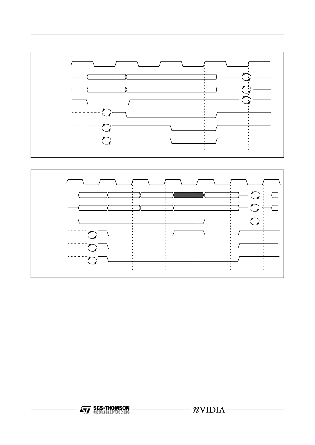
Figure 26.
SGRAM random read accesses within a page, read latency of two
1
NOTE
1 Covers either successive r eads to the active row in a given bank , or to the active rows in differen t banks. DQMs are all
activ e (L O W).
Figure 27.
SGRAM random read accesses within a page, read latency of three
1
NOTE
1 Covers eithe r successive reads t o t he active row in a given bank, or to the active rows i n different banks.
FBDQM
is all
activ e (L O W).
t
CL
CLK low time 3.5 4.5 - - ns
t
AS
Address setup time 3 4 - ns
t
AH
Address hold time 1 1 - ns
t
DS
Write data setup time 3 4 - ns
t
DH
Write data hold time 1 1 - ns
t
OH
Read data hol d tim e 3 3 - ns
t
AC
Read data access time 9 9 - ns
t
LZ
Data out low impe dance time 0 0 - ns
Symbol Parameter Min. Max. Unit Notes
-10 -12 -10 -12
read read read
data n data a
read nop nop
bank, col n bank, col a bank, col x bank, col m
data x data m
FBCLKx
Command
FBA[9:0]
FBD[63:0]
read read read
data n
read nop nop
bank, col n bank, col a bank, col x bank, col m
data a data x da ta m
nop
FBCLKx
Command
FBA[9:0]
FBD[63:0]
Page 33

128-BIT 3D MULTIMEDIA ACCELERATOR RIVA 128
33/77
Figure 28.
SGRAM read to write, read latency of three
Table 7.
SGRAM I/O timing parameters
Figure 29.
SGRAM random write cycles within a page
NOTE
1 Covers either successive writes to the active row in a given bank or to the active rows in different banks.
FBDQM
is active
(low).
Figure 30.
SGRAM write to read cycle
NOTE
1 A read latency of 2 is shown for illustration
Symbol Parameter Min. Max. Unit Notes
t
HZ
Data out high impedance time 4 10 ns
t
DS
Write data setup time 4 ns
t
HZ
t
DS
read nop nop
read data n
nop write
bank, col n
write data b
bank, col b
FBCLKx
TDDQM
Command
FBA[9:0]
FBD[63:0]
write write write write
data n data a data x data m
bank, col n bank, col a bank, col x bank, col m
FBCLKx
Command
FBA[9:0]
FBD[63:0]
write nop read nop nop nop
bank,
col n
bank,
col b
write
data n
write
data n
read
data b
FBCLKx
Command
FBA[9:0]
FBD[63:0]
Page 34

128-BIT 3D MULTIMEDIA ACCELERATORRIVA 128
34/77
Figure 31.
SGRAM read to precharge, read latency of two
NOTE
1
FBDQM
is active (low)
Figure 32.
SGRAM read to precharge, read latency of three
NOTE
1 FBDQM
is active (low)
Figure 33.
SGRAM Write to Precharge
nop active
bank(s) bank,row
data n
t
RP
read precharge nop
bank, col n
FBCLKx
Command
FBA[9:0]
FBD[63:0]
precharge nop nop active
bank(s) bank,
data n
t
RP
read
bank,
FBCLKx
Command
FBA[9:0]
FBD[63:0]
col n
row
write nop nop precharge nop nop acti ve
bank(s) row
t
RP
t
WR
bank, col n
write data n write data
n+1
FBCLKx
FBDQM#
Command
FBA[9:0
]
FBD[63:0 ]
Page 35

128-BIT 3D MULTIMEDIA ACCELERATOR RIVA 128
35/77
Figure 34.
SGRAM Active to Read or Write
Table 8.
SGRAM timing parameters
Symbol Parameter Min. Max. Unit Notes
t
CS
FBCSx, FBRAS#, FBCAS#, FBWE#
,
FBDQM
setup time
3ns
t
CH
FBCSx, FBRAS#, FBCAS#, FBWE#
,
FBDQM
hold time
1ns
t
MTC
Load Mode register command to command 2 t
CK
t
RAS
Active to Prechar ge command period 7 t
CK
t
RC
Active to Active command period 10 t
CK
t
RCD
Active to Read or W r ite delay 3 t
CK
t
REF
Refresh period ( 1024 cycles) 16 ms
t
RP
Precharge command per iod 4 t
CK
t
RRD
Active bank A to Activ e bank B command
period
3t
CK
t
T
Transition t ime 1 ns
t
WR
Write recovery time 2 t
CK
active nop nop
t
RCD
read or write
FBCLKx
Command
Page 36

128-BIT 3D MULTIMEDIA ACCELERATORRIVA 128
36/77
7 VIDEO PLAYBACK ARCHITECTURE
The RIVA 128 video playback architecture is designed to allow playbac k of CCIR PAL or NT SC
video formats with the highest quality while requiring the smallest vi deo surface. The implementation is optimized around the Windows 95 Direct
Video and ActiveX APIs, and supports the following features:
•
Accepts interlaced video fields:
- This allows the off-screen video surface to
consume less memory since only one field
(half of each frame) is stored. Double buffering between fields is done in hardware with
‘temporal averaging’ being applied based on
intraframing.
•
Linestore:
- To support high q uality video playback the
RIVA 128 memory controller and video overlay engine supports horizontal and vertical
interpolation using a 3x2 multitap interpolating filter with image sharpening.
•
YUV to RGB conversion:
- YUV 4:2:2 format to 24-bit RGB true-color
- Chrominance optimization/user control
•
Color key video composition
Figure 35.
Video scaler pipeline
YUV
Vertical
Interpolation
Filter
(Smooth/Sharpen)
Colo r Space
Conversion to 24 -b it
RGB
Horizontal
Interpolation
24-bit RGB
Video outpu t
Video windowing, merge
with graphics pixel pipeline
Linestore
Page 37

128-BIT 3D MULTIMEDIA ACCELERATOR RIVA 128
37/77
7.1 VIDEO SCALER PIPELINE
The RIVA 128 video scaler pipeline performs
stretching of video images in any arbitrary factor in
both horizontal and vertical directions. The video
scaler pipeline consists of the following stages:
1 Vertical stretching
2Filtering
3 Color space conversion
4 Horizontal stretching
Vertical stretching
Vertical stretching is p erformed on pixels prio r to
color conversion. The video scaler linearly interpolates the pixels in the vertical direction using an internal buffer which stores the previous line of pixel
informat ion.
Filtering
After vertical interpolation, the pixels are horizontally filtered using an edge-enhancement or a
smoothing filter. The edge-enhanc ement filter enhances picture transition information to prevent
loss of image clarity following the smoothing filtering stage. The smoothing filter is a low-pass filter
that reduces the noise in the source image.
Color space conversion
The video overlay pipel ine logic converts images
from YUV 4:2:2 for mat to 24-bit RGB true-color.
The default color conversion coefficients conver t
from YCrCb to gamma corrected RGB.
Saturation controls make sure that the conversion
does not exceed the output range. Four control
flags in the color converter provides 16 sets of color conversion coefficients to allow adjustment of
the hue and saturation. The brightness of each
R G B component can also be individually adjusted, similar to the brightness controls of the monitor.
Horizontal stretching
Horizontal stretching is done in 24-bit RGB space
after color conversion. Each component is linearly
interpolated using a triangle 2-tap filter.
Windowing and panning
Video images are clipped to a rectangular window
by a pair of registers specifying the position and
width.
By programming the video start address and the
video pitch, the video overlay logic als o supports a
panning window that can zoom into a portion of the
source image.
Video composition
With the color keying feature enabled, a programmable key in the graphics pi xel stream a llows s election of either the video or the graphics output on
a pixel by pixel basis. Color keying allows any ar bitrary portions of the video to overlay the graphics.
With color keying disabled and video overlay
turned on, the video output ov erlays the graphics
in the video window.
Interlaced video
The video overlay can display both non-interlaced
and interlaced video.
Traditional video overlay hardware typically drops
every other field of an interlaced video stream,
resulting in a low frame rate. Some solutions have
attempted to overcome the this problem by deinterlacing the fields into a single frame. This
however introduces motion artifacts. Fast moving
objects appearing in different positions in different
fields, when deinterlaced, introduces visible
artifacts which look like hair-like lines projecting
out of the object.
Page 38

128-BIT 3D MULTIMEDIA ACCELERATORRIVA 128
38/77
Figure 36.
Displaying 2 fields with 1:1 ratio
The
RIVA 128
video o ver la y ha nd les inte rl ace d vi deo by disp laying every field, at the o riginal frame
rate of the video (50Hz for PAL and 60Hz for
NTSC). The video scaling logic upscales
,
in the ver-
tical direction
, t
he luma components in each field
and
linearly interpolates
successive lines to pro-
duce the
missing lines of each field
. This in terp olat-
ed scale is applied such that
the full frame s ize
of
each fi el d
is stretched
to the desir ed heigh t.
The video scaler offsets the bottom field image by
half a source image line to ensure that both frames
when played back align vertically.
The vertical filtering results in a smooth high quality
video p layba ck.
Also by d
isplay ing bo th fie lds on e af-
ter an other
, any
motion artifacts often f ound in dein-
terlaced video output
are removed
, becau se the
pix-
els in each field are
displayed in the order
in whic h
the
original source was c aptured.
Line 10
Interpolat e d line
(Line 10 & 12)
Line 12
Line 11
Line 13
Interpolat e d line
(Line 11 & 13)
Frame 1 (Top field) Frame 2 (Bottom field)
Page 39

128-BIT 3D MULTIMEDIA ACCELERATOR RIVA 128
39/77
8 VIDEO PORT
The RIVA 128 Multimedia Accelerator introduces
a multi-function Video Port that has been desi gned
to exploit the bus mastering functionality of the
RIVA 128. The Video Port is compliant with a simplified ITU-R-656 video format with control of attached video devices performed through the RIVA
128 serial interface. Video Port support includes:
•
Windows 95 DirectMPEG API acceleration by
providing:
- Bus mastered compressed data transfer to
attached DVD and MPEG-2 decoders
- Local interrupt and pixel stream handling
- Hardware buffer management of compressed data, decompressed video pixel
data and decompressed audio streams
•
Supports popular video d ecoders including the
Philips SAA7111A, SAA7112, ITT 3225, and
Samsung KS0127. The Video Port initiates
transfers of video packets over the internal NV
bus to either on or off screen surfaces as defined in the DirectDraw and DirectVideo APIs.
•
Supports filtered down-scaling or decimation
•
Allows additional devices to be added
Figure 37.
Connections to multiple video modules
8.1 VIDEO INTERFACE PORT FEATURES
•
Single 8-bit bus multiplexing among four transfer types: video, VBI, host and compressed
data
•
Synchronous 40MHz address/data multiplexed
bus
•
Hardware-based round-robin scheduler with
predictable performance for all transfer types
•
Supports multiple video modules and one ribbon cable board on the same bus
•
ITU-R-656 Master Mode
•
Video Port
- Simplified ITU-R-656 Video Format -- supports HSYNC, VSYNC, ODD FIELD and
EVEN FIELD
- VBI data output from video decoder is c aptured as raw or sliced data
PCI/AGP
MPCLK
MPAD[7:0]
MPFRAME#
MPDTACK#
MPSTOP#
RIVA 128
Video
decoder
Media Port
Controller
(MPC)
S Video
VMI 1.4
ITU-R-656
DVD
Controller
TV tuner
SDA
SCL
Page 40

128-BIT 3D MULTIMEDIA ACCELERATORRIVA 128
40/77
8.2 BI-DIRECTIONAL MEDIA PORT POLLING
COMMANDS USING MPC
The Media Port transfers data using a Polling Protocol. The Media Port is enabled on the RIVA 128
by the host system software. The first cycle after
being enabled is a Poll Cycle. The MPC ASIC
must respond to every poll cycle with valid data
during DTACK active. If no transactions are needed, it responds with 00h. The Media Port will continue to Poll until a transaction is requested, or until there is a Host CPU a cces s to an external register.
Polling Cycle
Media Port initiates a Polling Cycle whenever
there is no pending transaction. This gives the
MPC ASIC a mechanism to ini tiate a transaction.
The valid Polling commands are listed in the Polling Command table. The priority for the polling requests should be to give the Display Data FIFO
highest priority.
CPU Register Write
Initiated by the Host system software.
CPU Register Read Issue
Initiated by the Host system software. The read
differs from the write in the fact that it must be done
in two separate transfers. The Read Issue is just
the initiation of the read cycle. The Media Port
transfers the address of the register to be read
during this cycle. After completion of the Read Issue cycle the media port goes back to polling for
the next transaction. When it receives a Read
Data ready command, it will start the next cycle in
the read.
CPU Register Read Receive
Initiated by the MPC ASIC when it h as read data
ready to be transferred to the media port. The
MPC ASIC waits for the next polling cycle and returns a Read Data R eady status. Th e media port
will transfer the read data on the next Read Receive Cycle. The PCI bus will be held off and retry
until the register read is complete.
Video Compressed Data DMA Write
Initiated by the MPC ASIC with the appropriate
Polling Command. The media port manages the
Video Compressed data buffer in system memory.
Each request for data will return 32 bytes in a single burst.
Display Data DMA Read
Initiated by the MPC ASIC with the polling command. The MPC ASIC initiates this transfer when
it wishes to tr ansfer video data in ITU-R-656 for mat.
Table 9.
Media Port Transactions
Table 10.
Polling Cycle Commands
A0 Cycle Transaction Description
11xx0000 Poll_Cycle Polling Cycle
00xx---- CPUWrite CPU Register Wr i t e
01xx1111 CPURead_ Is sue CPU Register Read I ssue
11xx1111 CPURead_ Re ceive CPU Register R ead R eceive
01xx0001 VCD_DMA_Write Video Compressed Data DMA Write
11xx1000 Display_Data_Read Display Data DMA Read
BIT Data Description
0 000xxxx1 NV_PME_VM I _PO LL_UNCD Request DMA Read of Display Data
1 000xxx1x NV_PME_VM I _PO LL_VIDCD Request DM A Wr i te of Video Compressed Data
3 000x1xxx NV_PME_VM I_POLL_INT Reque st for Interr upt
4 0001xxxx NV_PME_VM I _PO LL_CPURDREC Respond to Rea d Issue - Read Data Read y
00000000 NULL No T ransactions requested
Page 41

128-BIT 3D MULTIMEDIA ACCELERATOR RIVA 128
41/77
8.3 TIMING DIAGRAMS
Figure 38.
Poll cycle
Figure 39.
Poll cycle throttled by slave
Figure 40.
CPU write cycle
Figure 41.
CPU write cycle throttled by slave
A0 D0
MPCLK
MPFRAME#
MP_AD[7:0
]
MPDTACK#
A0 D0
MPCLK
MPFRAME#
MP_AD[7:0
]
MPDTACK#
A0 D
MPCLK
MPFRAME#
MP_AD[7:0
]
MPDTACK#
A1
A0 D
MPCLK
MPFRAME#
MP_AD[7:0
]
MPDTACK#
A1
Page 42

128-BIT 3D MULTIMEDIA ACCELERATORRIVA 128
42/77
Figure 42.
CPU read issue cycle - cannot be throttled by slave
Figure 43.
CPU read_receive cycle
Figure 44.
CPU read_receive cycle - throttled by slave
Figure 45.
CD write cycle - terminated by master
A0
MPCLK
MPFRAME#
MP_AD[7:0
]
A1/D
A0 D0
MPCLK
MPFRAME#
MP_AD[7:0
]
MPDTACK#
A0 D0
MPCLK
MPFRAME#
MP_AD[7:0
]
MPDTACK#
A0 D0 D1 D2 D3
MPCLK
MPFRAME#
MP_AD[7:0]
MPDTACK#
Page 43

128-BIT 3D MULTIMEDIA ACCELERATOR RIVA 128
43/77
Figure 46.
CD write cycle - terminated by slave in middl e of transfer
Figure 47.
CD write cycle - terminated by slave on byte 31
Figure 48.
CD write cycle - terminated by slave on byte 32, no effect
Figure 49.
UCD read cycle, terminated by master, throttled by slave
A0 D0 D1 D2 XXX A0 D3 D4
MPCLK
MPFRAME#
MP_AD[7:0]
MPDTACK#
MPSTOP#
A0 D0 D30 XXX A0 D31
MPCLK
MPFRAME#
MP_AD[7:0]
MPDTACK#
MPSTOP#
A0 D0 D30 D31
MPCLK
MPFRAME#
MP_AD[7:0]
MPDTACK#
MPSTOP#
A0 XXX D1 D2 D3D0
MPCLK
MPFRAME#
MP_AD[7:0]
MPDTACK#
Page 44

128-BIT 3D MULTIMEDIA ACCELERATORRIVA 128
44/77
Figure 50.
UCD read cycle, terminated by slave, throttled by slave
Figure 51.
UCD read cycle, slave termination after MPFRAME# deasserted, data taken
Figure 52.
UCD read cycle, slave termination after MPFRAME# deasserted, data not taken
Figure 53.
UCD read cycle, slave termination after MPFRAME# deasserted, data taken
A0 XXX D1 D2D0
MPCLK
MPDTACK#
MPSTOP#
MPFRAME#
MP_AD[7:0]
A0 D1 D2 D3D0
MPCLK
MPFRAME#
MP_AD[7:0]
MPDTACK#
MPSTOP#
A0 D1 D2 D3D0
MPCLK
MPFRAME#
MP_AD[7:0]
MPDTACK#
MPSTOP#
A0 D1 D2D0
MPCLK
MPFRAME#
MP_AD[7:0]
MPDTACK#
MPSTOP#
Page 45

128-BIT 3D MULTIMEDIA ACCELERATOR RIVA 128
45/77
8.4 656 MASTER MODE
Table 11 shows the Video Port pin definition when
the RIVA 128 is configured in ITU-R-656 Master
Mode. Before entering this mode, RIVA 128 disables all Video Port devices so that the bus is tristated. The RIVA 128 will then enable the video
656 master device through the serial bus. In this
mode, the video device outputs the video data
continuously at the PIXCLK rate.
Table 11.
656 master mode pin definition
The 656 Master Mode assumes that
VID[7:0]
and
PIXCLK
can be tri-stated wh en the slave is inactive. If a slave cannot tri-state all its signals, an external tri-state buffer is needed.
Video data capture
Video Port pixel data is clocked into the port by the
external pixel clock and then passed to the RIVA
128's video capture FIFO.
Pixel data capture is controlled by th e ITU-R-656
codes embedded in the data stream; each active
line beginning with SAV (start active video) and
ending with EAV (end active video).
In normal operation, when SAV = x00, capture of
video data begins, and when EAV = xx1, capture
of video data ends for that line. When VBI (Vertical
Blanking Interval) capture is active, these rules are
modified.
656 master mode timing specification
Figure 54.
656 Master Mode timing diagram
Table 12.
ITU-R-656 Master Mode timing parameters
NOTE
1
VACTIVE
indicates that valid pixel data is being transmitted across the video por t.
Table 13.
YUV (YCbCr) byte ordering
Normal Mode 656 Master M ode
MPCLK PIXCLK
MPAD[7:0] VID[7:0]
MPFRAME#
Not used
MPDTACK#
Not used
MPSTOP#
Not used
Symbol Parameter Min. Max. Unit Notes
t
3
VID[7:0]
hold from
PIXCLK
high 0 ns
t
4
VID[7:0]
setup to
PIXCLK
high 5 n s
t
5
PIXCLK
cycle time 35 ns
1st byte 2nd byt e 3rd byte 4th byte 5th (next
dword)
6th byte 7th byte
U[7:0] Y0[7:0] V[7:0] Y1[7:0] U[7:0] Y0[7:0] V[7:0]
Cb[7:0] Y0[7:0] Cr[7:0] Y1[7:0] Cb[7:0] Y0[7:0] Cr[7:0]
t
5
t
4
t
3
t
4
t
3
t
4
t
3
PIXCLK
VID [ 7:0]
Page 46

128-BIT 3D MULTIMEDIA ACCELERATORRIVA 128
46/77
8.5 VBI HANDLING IN THE VIDEO PORT
RIVA 128 supports two basic modes for VBI data
capture. VBI mode 1 is for use with the Philips
SAA7111A digitizer, VBI mode 2 is for use with the
Samsung KS0127 digitizer.
In VBI mode 1, the region to be captured as VBI
data is set up in the SAA7111A via the serial interface, and in the RIVA 128 under software control.
The SAA7111A responds by suppressing generation of SAV and EAV codes for the lines selected,
and sending raw sample data to the port. The
RIVA 128 Video Port capture engine starts capturing VBI data at an EAV code in the line last active
and continues to capture data without a break until
it detects the next SAV code. VBI capture is then
complete for that field.
In VBI mode 2, the region to be captured as VBI
data is set up in a similar manner. The KS0127 responds by enabling VBI data collection only during
the lines specified and framed by normal ITU-R656 SAV/EAV codes. The RIVA 128 Video Port
capture engine starts capturing data at an SAV
code controlled by the device driver, and continues capturing data under control of SAV/EAV
codes until a specific EAV code identified by the
device driver is sampled. VBI capture is then complete for that field. The number of bytes collected
will vary depending on the setup of the KS0127.
8.6 SCALING IN THE VIDEO PORT
The RIVA 128 Video Port allows any arbitrary
scale factor between 1 and 31. For best results the
scale factors of 1, 2, 3, 4, 6, 8, 12, 16, and 24 are
selected to avoid filtering losses. The Video Port
decimates in the y-direction, dropping line s every
few lines depending on the vertical s caling factor.
The intention is to support filtered dow nscaling in
the attached video decoder.
Page 47

128-BIT 3D MULTIMEDIA ACCELERATOR RIVA 128
47/77
9 BOOT ROM INTERFACE
BIOS and initialization code for the RIVA 128 is accessed from a 32KByte ROM. The RIVA 128 memory
bus interface signals
FBD[15:0]
and
FBD[31:24]
are used to address and access one of 64KBytes of data
respectively. The unique decode to the ROM device is provided by the
ROMCS#
chip select signal.
Figure 55.
ROM interface
ROM interface timing specification
Figure 56.
ROM interface timing diagram
FBD[15:0]
FBD[31:24]
ROMCS#
D[7:0]
A[15:0]
CS
ROM
WE
RIVA 128
FBD[17]
OE
FBD[16]
ROM Read
t
BAS
t
BRCS
t
BAH
t
BRCA
t
BRV
t
BRH
t
BDBZ
t
BDS
t
BDH
t
BDZ
t
BOS
address
data
FDB[15:0]
ROMCS#
OE# (FBD[16] )
WE# (FBD[1 7 ])
FDB[31:24]
ROM Write
t
BAS
t
BRCS
t
BAH
t
BWDS
t
BWDH
address
data
FDB[15:0]
ROMCS#
OE# (FBD[16] )
WE# (FBD[1 7 ])
FDB[31:24]
t
BWS
t
BWL
t
BOH
Page 48

128-BIT 3D MULTIMEDIA ACCELERATORRIVA 128
48/77
Table 14.
ROM interface timing parameters
NOTE
1T
MCLK
is the period of the internal memory clock.
2 This parameter is programmable in the range 0 - 3 MCLK cycles
3 This parameter is programmable in the range 0 - 15 MCLK cycles
Symbol Parameter Min. Max. Unit Notes
t
BRCS
ROMCS#
active pul s e w idth 20T
MCLK
-5 ns
t
BRCA
ROMCS#
precharge time T
MCLK
-5 ns
t
BRV
Read valid to
ROMCS#
active T
MCLK
-5 ns
t
BRH
Read hold from
ROMCS#
inactive T
MCLK
-5 ns
t
BAS
Address setup to
ROMCS#
active T
MCLK
-5 ns
t
BAH
Address hold from
ROMCS#
inactive T
MCLK
-5 ns
t
BOS
OE# lo w from
ROMCS#
active ns 2
t
BOH
OE# lo w to
ROMCS#
inactive ns 3
t
BWS
WE# low from
ROMCS#
active ns 2
t
BWL
WE# low time ns 3
t
BDBZ
Data bus high-z to
ROMCS#
active T
MCLK
-5 ns
t
BDS
Data setup to
ROMCS#
inactive 10 ns
t
BDH
Data hold from
ROMCS#
inactive 0 ns
t
BDZ
Data high-z from
ROMCS#
inactive T
MCLK
-5 ns
t
BWDH
Write data hold fro m
ROMCS#
inactive 0.5T
MCLK
-5 ns
t
BWDS
ROM write data setup to
ROMCS#
active T
MCLK
-5 ns
Page 49

128-BIT 3D MULTIMEDIA ACCELERATOR RIVA 128
49/77
10 POWER-ON RESET CONFIGURATION
The RIVA 128 latches its configuration on the trailing edge of
RST#
and holds its system bus interface in a high impedance state until this time. To
accomplish this, pull-up or pull-down resistors are
connected to the
FBA[9:0]
pins as appropriate.
Since there are no internal pull-up or pull-down resistors and the data bus should be floating during
reset, a resistor value of 47KΩ should be sufficient.
Power-on reset FBA[9:0] bit assignments
[9]
PCI Mode. This bit indicates whether the
RIVA 128
initializes with PCI 2.1 compliance
0 = RIVA 128 is PCI 2.0 compliant (does not support delayed transactions)
1 = RIVA 128 is PCI 2.1 compliant (supports 16 clock target latency requirement).
[8:7]
TV Mode. These bits select the timing format when TV mode is enabled.
00 = Reserved
01 = NTSC
10 = PAL
11 = TV mode disabled
[6]
Crystal Frequency. This bit should match the frequency of the crystal or reference clock connected to
XTALOUT
and
XTALIN
.
0 = 13.500MHz (used where TV output may be enabled)
1 = 14.31818MHz
[5]
Host Interface
0 = PCI
1 = AGP (Bit 0 must also be pulled high to indicate 66MHz)
[4]
RAM Width
0 = 64-bit framebuffer data bus width (the upper 64-bit data bus and byte selects are tri-state)
1 = 128-bit framebuffer data bus width
[3:2]
RAM Type
00 = Reserved
01 = 8Mbit SDRAM or SGRAM organized as 128K x 2 banks x 32-bit (normal SGRAM mode).
10 = Reserved
11 = 8Mbit SDRAM or SGRAM organized as 128K x 2 banks x 32-bit, framebuffer I/O pins remain
tri-stated after reset.
[1]
Sub-Vendor. This bit indicates whether the PCI Subsystem Vendor field is located in the system
motherboard BIOS or adapter card VGA BIOS. If the Subsystem Vendor field is located in the system BIOS it must be written by the s ystem BIOS to the PCI c onfiguration spac e prior to running
any PnP code.
0 = System BIOS (Subsystem Vendor ID and Subsystem ID set to 0x0000)
1 = Adapter card VGA BIOS (Subsystem Vendor ID and Subsystem ID read from ROM BIOS at
location 0x54 - 0x57)
[0]
Bus Speed. This bit indicates the value returned in the 66MHZ bit in the PCI Configuration registers (see page 64).
0 = RIVA 128 PCI interface is 33MHz
1 = RIVA 128 is 66MHz capable
9876543210
PCI
Mode
TV Mode Crystal Host
Interface
RAM
Width
RAM Type Sub-
Vendor
Bus
Speed
Page 50

128-BIT 3D MULTIMEDIA ACCELERATORRIVA 128
50/77
The following example configuration is shown in Fi gure 57:
•
Subsystem Vendor ID initialized to 0 and writeable by system BIOS (see Appendix A, page 70)
•
8Mbit 128K x 2 bank x 32 SGRAM
•
128-bit framebuffer interface
•
AGP including 66MHz PCI 2.1 compliant subset
•
Using 13.5000MHz crystal
•
TV output mode is NTSC
Figure 57.
Example motherboard configuration
10K
Ω
10K
Ω
RIVA 128
FBA[1
]
FBA[2]
FBA[3]
SGRAM
array
VDD (3.3V)
AGP
FBA[4]
FBA[5]
FBA[8]
FBA[6]
FBA[7]
FBA[0
]
FBA[9]
FBA[10]
Page 51

128-BIT 3D MULTIMEDIA ACCELERATOR RIVA 128
51/77
11 DISPLAY INTERFACE
11.1 PALETTE-DAC
The Palette-DAC integrated into the RIVA 128
supports a traditional pixel pipeline with the following enhancements:
•
Support for 10:10:10, 8:8:8, 5:6:5 a nd 5:5:5 direct color pixel modes
•
Support for dynamic gamma correction on a
pixel by pixel basis
•
Support for mixed indexed color and direct color pixels
•
256 x 24 LUT for 8-bit indexed modes
•
High quality video overlay
- Accepts interlaced video fields allowing a reduction in memory buffering requirements while
incorporating temporal averaging
- Line buffer for horizontal and vertical interpolation of video streams up to square pixel PAL
resolution
- 3x2 multitap interpolating filter with image
sharpening
- Color key in all color pixel modes
- High quality YUV to RGB conversion with
chrominance control.
11.2 PIXEL MODES SUPPORTED
8-bit indexed color
In the 8-bit indexed color each 32-bit word contains four 8-bit indexed color pixels, each comprising bits
b[7:0] as shown below.
NOTE
1 This 32-bit representation can be extended to 64-bi t and 128-bit widths by dupli cating the 32-bit word in little-endian form at.
16-bit direct color modes (5:6:5 direct and 5:5:5 with and without gamma correction)
In 5:5:5 color modes bit 15 of each pixel can be enabled to select whether pixel data bypasses the LUT to
feed the DACs directly, or indirectly, through the LUT, to allow gamma correction to be applied. If not enabled then the bypass mode will always be selected, and the LUT powered down. The 16-bit modes include a 5:6:5 format which always by passes the LUT.
NOTE
1 This 32-bit representation ca n be ext ended to 64-bit and 128-bit widths by dup licatin g the 32-bit word in little-en dia n for-
mat.
32-bit direct color (8:8:8 with gamma correction or 10:10:10 direct)
In 32-bit color mode bit 31 of each pixel selects whethe r pixel data bypasses the LUT , to feed the DACs
directly or indirectly, through the LUT, to allow gamma correction to be applied. In the table below the Red,
Green and Blue bypass bits are shown individually as R[9:0], G[9:0], and B[9:0] because, in the bypass
Pixel formats (FBD[31:0])
31 30 29 28 27 26 25 24 23 22 21 20 19 18 17 16 15 14 13 12 11 10 9 8 7 6 5 4 3 2 1 0
Pixel 3Pixel 2Pixel 1Pixel 0
b7 b6 b5 b4 b3 b2 b1 b0 b7 b6 b5 b4 b3 b2 b1 b0 b7 b6 b5 b4 b3 b2 b1 b0 b7 b6 b5 b4 b3 b2 b1 b0
5:6:5
mode
Pixel formats (FBD[31:0])
Pixel 1 P ixel 0
313029282726252423222120191817161514131211109876543210
0 0 Red gamma Green ga m ma Blue gam m a 0 Red gamma Green gamm a Blu e gam m a
0 1 Red bypass Green bypass Blue bypass 1 Red bypass Green bypass Blue bypass
1 Red bypass Green bypass Blue bypass Red bypass Green bypass Blue bypass
Page 52

128-BIT 3D MULTIMEDIA ACCELERATORRIVA 128
52/77
mode pixel format, the least significant bits of each color are located separately in the top byte of the pixel.
This also permits an 8:8:8 mode without gamma with <1% error if desired.
NOTE
This 32-bit representation can be extended t o 64-bit and 128-bit widths by duplicati ng the 32-bit word in little-endian format .
Limitations on line lengths
Table 15.
Permitted line length multiples
11.3 HARDWARE CURSOR
The RIVA 128 supports a 32x32 15bpp full color
hardware cursor as defined by Microsoft Windows.
•
Full color 5:5:5 format
•
Pixel complement
•
Transparency
•
Pixel inversion
The cursor pattern is stored in a 2KByte bitmap located in off-screen framestore. Details of programming the hardware cursor are given in the RIVA
128
Programming Reference Manual
[2]. Registers control cursor enabling/disabling, location of
cursor bitmap and cursor display coordinates. The
cursor data and it's position should only be
changed during frame flyback. The cursor should
be disabled when not being used.
Cursor format
The 5-bit RGB color components are expanded to
10 bits per color before combining with the graphics display data. The expanded 10-bit color is composed of the 5-bit cursor color replicated in the upper and lower 5-bit fields. The cursor pixels are
combined such that the cursor will overlay a video
window if present.
Cursor pixel bit 15 (A) is the replace mode bit.
When A=1, the cursor pixel replaces the normal
display pixel. If A=0, the e xpanded 30 bits of the
cursor color are XORed with the display pixel to
provide the complement of the background color.
Cursor pixels can be made transparent (normal
display pixel is unmodified) by setting to a value of
0x0000. To invert the bits of the normal display
pixel, the cursor pixel should be set to 0x7FFF.
Use of pixel in put pins (FBD [31:0])
Pixel 0
31 30 29 28 27 26 25 24 23 22 21 20 19 18 17 16 15 14 13 12 11 10 9 8 7 6 5 4 3 2 1 0
0 X X X X X X X Red gamma Green gamma Blue gamma
1X
R1 R0 G1 G0 B1 B0 R9 R8 R7 R6 R5 R4 R3 R2 G9 G8 G7 G6 G5 G4 G3 G2 B9 B8 B7 B6 B5 B4 B3 B2
bpp 8 16 32
Number of pixels that the line
length must be a mult ipl e of
421
1514131211109876543210
A Red Green Blue
Page 53

128-BIT 3D MULTIMEDIA ACCELERATOR RIVA 128
53/77
11.4 SERIAL INTERFACE
The RIVA 128 serial interface supports connection
to DDC1/2B, DDC2AB and DDC2B+ compliant
monitors and to serial interface controlled video
decoders and tuners. Supported video decoder
chips include Philips SAA7110, SAA7111A, ITT
3225 and Samsung KS0127. For details of address locations and protocols applying to specific
parts refer to the appropriate manufacturer’s
datasheet.
The serial interface in RIVA 128 requires operation
under software control to provide emulation of the
interface standard. RIVA 128 can act as a master
for communication with slave devices like those
mentioned above. It also acts as a master when interfacing to a DDC1/2 compatible monitor. Although it is not Access.bus compatible, it c an communicate with a DDC2AB compati ble monitor via
the DDC2B+ protocol. (No other Access.bus peripherals can be attached although other serial devices may co-reside on the DDC bus). The RIVA
128 can clock stretch incoming messages in the
event that the software handl er is interrupted by
another task.
Page 54

128-BIT 3D MULTIMEDIA ACCELERATORRIVA 128
54/77
11.5 ANALOG INTERFACE
Figure 58.
Recommended circuit (crystal circuit is for designs not supporting TV out)
Table 16.
Table of parts for recommended circuit (Figure 58)
Part number Value Description
C1 22µF tanta lum capacitor
C2 100nF surface mount capacitor
C3, C4 22pF surface mount capacitor
C5, C6 10nF surface mount capacitor
R1 147Ω 1% resis tor
R2-R4 75 Ω 1% resist or
D1-D6 1N4148 protection diodes
L1 1µH inductor
X1 13.50000 MHz s er ies resonant crystal (used whe r e TV ou tp ut may be
required)
14.31818MHz s er ies resonant crystal
C2
Monitor
RSET
PLLVDD
VDD
GND
VDD
Local PLLVDD plane
∗
∗
L1
75Ω
∗ These components should be placed as close to the RIVA 128 outputs as possible
75Ω
cable
D1-D3
Power supply
C1
C5
R1
R2-R4
D4-D6
∗
XTALIN
C3
C4
X1
∗
COMP
RED,
GREEN,
BLUE
XTALOUT
RIVA 128
VREF
C6
DACVDD
Page 55

128-BIT 3D MULTIMEDIA ACCELERATOR RIVA 128
55/77
11.6 TV OUTPUT SUPPORT
Reference clock options
The RIVA 128 supports two synthesizer reference
clock frequencies; 13.5MHz and 14.31818MHz.
The reference clock frequency is determined by a
crystal or reference clock connected to the
XTA-
LIN
and
XTALOUT
pins. Where TV-out is support-
ed,
XTALOUT
should be driven by a 13.5MHz reference clock derived from an external NTSC/PAL
clock source as illustrated in Figure 59. The clock
frequency should match the power-on configuration setting described in Section 10, page 49.
PAL/NTSC TV interface
The RIVA 128 suppor ts TV outpu t thro ugh an external Analog Devices AD722 PAL/NTSC RGB
encoder chip as shown in Figure 59. A MicroClock
MK2715 NTSC/PAL clock chip provides a common source for synchronization of the pixel and
subcarrier clocks. In TV output modes the RIVA
128
XTALOUT
pin must be externally driven from
the MK2715 reference clock output, with
XTALIN
tied to GND.
The MK2715 requires a number of external com-
ponents for proper operation. F or crystal input a
parallel resonant 13.5000MHz crystal is recommended, with a frequency tolerance of 50ppm or
better. Capacitors shoul d be connected from X1
and X2 to GND as shown in Figure 59. Alternatively a clock input (e.g. ClockCan) can be connected
to X1, leaving X2 disconnected. Further details are
given in the MK2715 datasheet [8].
Figure 59.
TV output implementation
75
Ω
75
Ω
75
Ω
RIVA 128
R
G
B
VIDHSYNC
AD722 TV
RGB Encoder
RIN
GIN
BIN
HSYNC
FIN
YOUT
COUT
CVOUT
220µF
220µF
220µF
75
Ω
MK2715
NTSC/PAL
Clock Source
33
Ω
4XCLK
REFOUT
XTALOUT
XTALIN
33
Ω
330
Ω
220
Ω
5V
27pF
27pF
13.50000MHz
crystal
X1/ICLK
X2
Page 56

128-BIT 3D MULTIMEDIA ACCELERATORRIVA 128
56/77
Figure 60.
Interface to monitor or television
Monitor detection
Figure 60 shows the typical connection of a television or computer mo nitor to the RIVA 128s’ D AC
outputs. The RIVA 128 expects only one output
display device to be connected at a time and does
not support simultaneous output to both the monitor and television.
During system initializati on, the BIOS detec ts if a
monitor is connected by sensing the doubly-terminated 75Ω load (net 37.5Ω). When no monitor is
connected, only the local 75Ω load is detected and
the RIVA 128 switc hes to television o utput mod e.
The BIOS sets the CRTC registers to generate the
appropriate timing for the local television standard
and the DACs are adjusted to compensate for the
single 75Ω load.
Monitor mode is always selected if a monitor is detected since it is assumed to be the output device
of choice, having a higher display fidelity than television.
Timing generation
Televisions contain two Phase-Locked Loops
(PLLs). One PLL locks the horizontal frequency
and is used to synchronize horizontal and vertical
flyback, and to keep the active video region stable
and centered. The second PLL locks the color
subcarrier frequency (NTSC 3.5794545MHz or
PAL 4.43361875MHz). The color subcarrier is
used as a phase referenc e to extract the color information from the television signal.
The RIVA 128 encodes horizontal and vertical timing on a composite sync signal. Using a
13.5000MHz reference clock, the RIVA 128 timing
generator creates ITU-R-601 NTSC and PAL
compliant horizontal timing with only ppm (parts
per million) error. The RIVA 128 does not use the
color subcarrier clock internally. The reference
clock source can be located on the television upgrade module with the video encoder and TV output connectors, thus lowering the base system
cost.
Flicker filter
RIVA 128 provides an optional flicker filtering feature for TV and interlaced displays.
Without flicker filtering, elements of an image
present on either the odd or the even field, but not
both, are seen to flicker or shimmer obtrusively.
This is a problem especially with 1-pixel-wide horizontal lines often or iginating from compute r generated GUI displays.
Flicker filtering causes a slight smearing of pixels
in the vertical direction. This trades off image quality versus flicker. The displayed pixel contains a
proportion of the data for the pixel on that line, plus
a smaller proportion of the data of the equivalent
pixel on the line above and on the line below.
Overall, the proportions add up to 1 so that the
brightness of the screen does not alter and the pixel data does not get clipped.
Flicker filtering only takes place on pixel data from
the framestore - the pattern written into the cursor
already has flicker removed. No flicker removal i s
performed on video images.
Overscan and underscan
The RIVA 128 supports overscan and underscan
in the horizontal and vertical directions using hardware scaling. Undersc an allows 640x480 resolution to fit onto NTSC displays and 800x600 resolution to fit onto PAL displays. Scaling can be adjusted and controlled by softwar e to suit specific TV
requirements. The TV output image position is
also software controllable.
RIVA 128
R
G
B
75 75 75
Monitor
R
G
B
Y
C
Y/C
TV RGB
Encoder
PAL/NTSC
Television
75
75
75
75 75 75
Page 57

128-BIT 3D MULTIMEDIA ACCELERATOR RIVA 128
57/77
12 IN-CIRCUIT BOARD TESTING
The RIVA 128 has a number of features designed to support in-circuit board testing. These include:
•
Dedicated test mode input and dual-function test mode select pins selecting the following modes:
- Pin float
- Parametric NAND tree
- All outputs driven high
- All outputs driven low
•
Checksum test
•
Test registers
12.1 TEST MODES
Primary test control is provided by the dedicated
TESTMODE
input pin. The RIVA 128 is in normal oper-
ating mode when this pin is deass erted. When
TESTMODE
is asserted,
MP_AD[3:0]
are reassigned as
TESTCTL[3:0]
respectively. Test modes ar e selected asyn chronously through a c ombination of the pin
states shown in Table 17.
Table 17.
Test mode selection and descriptions
12.2 CHECKSUM TEST
The RIVA 128 hardware checksum feature supports
testin g of th e enti r e pix el dat a path a t full v id eo ra t es
from t he fram ebuff er throu gh to the DA C inputs . Each
of the thr ee RG B co lo rs c an be t ested t o pr ovid e a
correlation between the intended and actual display.
Checksums are accumulated during active (unblanked) display. Note that the checksum mechanism does not check the DAC outputs (i.e. what is
physically being displayed on the monitor).
For a given image (which can be a real application’s
image or a specially prepared test card), theoretically derived checksum values can be calculated for a
selected RGB color, which are then c ompared with
the RIVA 128 hardware checksum value. Alternatively the checksum value fro m a known good chip can
be used as the reference.
Hardware checksum accumulation is not affected by
the horizontal and vertical synchronization waveforms or timings. Any discrepancy between the calculated and RIVA 128 hardware accumulated checksum values therefore indicates a problem in the
device or sys tem being teste d. Deta ils of p rogramming the RIVA 128 checksum are given in the RIV A
128
Programming Reference Manual
[2].
Test mode TESTCTL[3:0] Description
3210
Parametric
NAND tree
1 0 1 0 A single parametr ic N AN D tree is provided to give a quiescent environ-
ment in which to test V IL and VIH without requir ing core activity.
This capabili ty is provided in t he pads by chaining all I and I/O paths to -
gether via tw o input N AND gates. The chain be gi ns with on e input of the
first NAND gate tied to VDD while th e ot her input i s connected to t he first
device pin on the NAND tree. The output of this gate then becomes the input of the next NA ND gate in t he t r ee and so on until all pa d input paths
have been connected. The final NAND gate output is connected to an output-only pin whose normal functionality is disabled in NAND tree mode.
The NAND t re e le ngth is the refore eq u al to the number of I and I/O pins in
the RIVA 128. Output -only pins are not connected into the NAND tree.
Pin float 1 1 0 0 All pin output drivers are tr istated in this test mode so t hat pin leakage
current (IIL,IIH,IOZL,IOZH) can be measured.
Outputs high 1 1 1 0 All pin output drivers drive a high output state in thi s test mode so that
output high voltage (VOH at IOH) can be measured.
Outputs low 1 1 1 1 All pin output drivers drive a low output state in this test mode so that out-
put low voltage (VOL at IOL) can be measured.
Page 58

128-BIT 3D MULTIMEDIA ACCELERATORRIVA 128
58/77
13 ELECTRICAL SPECIFICATIONS
13.1 ABSOLUTE MAXIMUM RATINGS
1
NOTES
1 Stresses greater tha n th ose l isted under ‘ Absol ut e ma xi mum r atings’ may cause perm anent damage to the devi ce. Thi s
is a stress rating only and functional operation of the device at these or any other conditions above those indicated in the
operational sections of this specification is not implied. Exposure to absolute maximum rating conditions for extended periods may affect reliability.
2 For 3V tolerant pins VDD = 3.3V ± 0.3V, for 5V tolerant pins (PCI, Video Port and Serial interfaces) VDD = 5V ± 0.5V
13.2 OPERATING CONDITIONS
13.3 DC SPECIFICATIONS
Table 18.
DC characteristics
NOTES
1 Includes high impedance output leakage for all bi-directional buffers with tri-state outputs
2 VDD = max, GND ≤ VIN ≤ VDD
Table 19.
Parameters applying to PCI and AGP interface pins
Symbol P arameter Min. Max. Units Notes
VDD/AVDD DC supply voltag e 3.6 V
Voltage on input and output pins G ND-1.0 VDD +0. 5 V 2
TS Stora ge t em per ature (ambient) -55 12 5 °C
TA Temper at ur e under bias 0 85 °C
Analog output current (per output) 45 mA
DC digital output current (per out put) 25 mA
Symbol Parameter Min. Typ. Max. Units Notes
TC Case temperature 120 °C
Symbol Parameter Min. Typ. Max. Units Notes
VDD Positive supply voltage 3.135 3.3 3.465 V
IIN Input current (signal pins) ±10 µA1, 2
Power dissipation 3.7 W
Symbol Parameter Min. Typ. Max. Units Notes
CIN Input capacitance 5 10 pF 1
COUT Output load capacitance 5 50 pF 1
Parameters for 5V signaling environment only:
VIH Input logic 1 voltage 2.0 5.75 V
VIL Inpu t logic 0 vo l tage -0. 5 0.8 V
VOH Output logic 1 level 2.4 V
VOL Output logic 0 lev el 0.55 V
IOH O utput load cur rent, logic 1 level -2 mA
IOL Out put load current, logic 0 level 3 or 6 mA 2
Parameters for 3.3V and AGP signaling environments onl y:
VIH Input logic 1 voltage 0.475VDD VDD+0.5 V
Page 59

128-BIT 3D MULTIMEDIA ACCELERATOR RIVA 128
59/77
NOTE
1 Tested but not guaranteed.
2 3mA for all signals except
PCIFRAME#, PCITRDY#, PCIIRDY#, PCIDEVSEL#
and
PCISTOP#
which have IOL of 6mA.
13.4 ELECTRICAL SPECIFICATIONS
Table 20.
Parameters applying to all signal pins except PCI/AGP interfaces
NOTE
1 Tested but not guaranteed.
2 For 3V tolerant pins VDD = 3.3V ± 0.3V, for 5V tolerant pins (Video Port and Serial interfaces) VDD = 5V ± 0.5V
13.5 DAC CHARACTERISTICS
VIL Input logic 0 voltage -0.5 0.325VDD V
VOH Output logic 1 level 0.9VDD V
VOL Output logic 0 lev el 0.1VDD V
IOH O utput load cur rent, logic 1 level -0.5 mA
IOL Out put load current, logic 0 level 1.5 mA
Symbol Parameter Min. Typ. Max. Units Notes
CIN Input capacitance 10 12 pF 1
COUT Output load capacitance 10 50 pF 1
VIH Input logic 1 vo ltage 2.0 VDD+0. 5 V 2
VIL Inpu t logic 0 vo l tage -0. 5 0.8 V
VOH Output logic 1 level 2.4 V
VOL Output logic 0 lev el 0.4 V
IOH O utput load cur rent, logic 1 level -1 mA
IOL Out put load current, logic 0 level 1 mA
Parameter Min. Typ. Max. Units Notes
Resolution 10 bits
DAC operating frequency 230 MH z
White relative to Black current 16.74 17.62 18.50 m A 2
DAC to DAC matc hing ± 1 ±2.5 % 2,4
Integral linearity ±0.5 ±1.5 LSB
8
2,3,8
Differential linearity ±0.25 ±1LSB
8
2,3,8
DAC output voltage 1.2 V 2
DAC output impedance 20 kΩ
Risetime (bl a c k to white leve l) 1 3 ns 2,5 ,6
Settling time (black to white) 5.9 ns 2,5,7
Glitch energy 50 100 pVs 2,5
Comparator trip voltage 280 335 420 mV
Comparator settling time 100 µs
Internal Vref voltage 1.235 V
Internal Vref voltage accuracy ± 3 ±5%
Symbol Parameter Min. Typ. Max. Units Notes
Page 60

128-BIT 3D MULTIMEDIA ACCELERATORRIVA 128
60/77
NOTES
1 Blanking pedestals are not supported in TV output mode.
2 VREF = 1.235V, RSET = 147
Ω
3LSB
8
= 1 LSB of 8-bit resolution DAC
4 About the midpoint of the distribution of the three DACs
5 37.5ohm, 30pF load
6 10% to 90%
7 Settling to within 2% of full scale deflection
8 Monotonicity guaranteed
13.6 FREQUENCY SYNTHESIS CHARACTERISTICS
NOTE
1 A series resonant crystal sho uld be con nected to
XTALIN
2 The pixel clock can be programm ed to within 0.5% of any target frequency 10 ≤ f
pixclk
≤ 230MHz
3 The maximum pixel clock fr equenc y whe n the RIVA 128 is disp laying full motion video
Parameter Min Typ. Max Units Notes
XTALIN
crystal frequency range 4 15 MHz 1
Internal VCO frequency 128 256 MHz
Memory clock output frequency 100 MHz
Pixel clock outpu t fre quency 230 MHz 2
Pixel clock outpu t fre quency (video displ ayed) 110 MHz 3
Synthesize r lock tim e 500 µs
Page 61

128-BIT 3D MULTIMEDIA ACCELERATOR RIVA 128
61/77
14 PACKAGE DIMENSION SPECIFICATION
14.1 300 PIN BALL GRID ARRAY PACKAGE
Figure 61.
RIVA 128 300 Plastic Ball Grid Array Package dimension reference
Table 21.
RIVA 128 300 Plastic Ball Grid Array Package dimension specification
Ref.
Millimeters Inches
Typ. Min. Max. Typ. Min. Max.
A 2.125 2.595 0.083 0.102
A1 0.50 0.70 0.020 0.027
A2 1.625 1.895 0.064 0.074
b 0.60 0.90 0.024 0.035
D 27.00 26.82 27.18 1.063 1.055 1.070
D1 24 .13 Basic 0.951 Basic
D2 23.90 24.10 0.941 0.949
e 1.27 Basic 0.050 Basic
E 27.00 26. 82 27 .18 1.063 1.055 1.070
E1 24.13 Basic 0.951 Basic
E2 23.90 24.10 0.941 0.949
All dimensions in mm unless otherwise noted
tolerances unless otherwise noted (mm)
0 ≤ 10 >10 ≤ 50 >50 ≤ 200 >200
±
0.05
±
0.1
±
0.15
±
0.25
D2
E2
A1
C
20 19 18 17 16 1514 13 12 11 10 9 8 7 6 5 4 3 2 1
A
B
C
D
E
F
G
H
J
K
L
M
N
P
R
T
U
V
W
Y
E
D
A
B
D1
e
E1
e
(4x)
b
SOLDER BALL (Typ)
0.250
A2
A
0.300 C A B
0.100SC
S
S S
C
0.350 C
0.150 C
0.200
e
e
Pin 1 indicator
Page 62

128-BIT 3D MULTIMEDIA ACCELERATORRIVA 128
62/77
15 REFERENCES
1 RIVA 128
Turnkey Manufacturing Package TMP, Design Guide
, NVIDIA Corp./SGS-THOMSON Micro-
electronics
2 RIVA 128
Programming Reference Manual,
NVIDIA Corp./SGS-THOMSON Microelectronics
3 Accelerated Graphics Port Interface Specification, Revision 1.0
, Intel Corporation, July 1996
4
PCI Local Bus Specification, revision 2.1
, PCI Special Interest Group, June 1995
5 Recommendation 656 of the CCIR, Interfaces for digital component video signals in 525-line and 625-
line television systems
, CCIR, 1990
6
Display Data Channel (DDC™) standard, Version 2.0, revision 0
, Video Electronics Standards Associ-
ation, April 9th 1996 (Video Electronics Standards Association - http://www.vesa.org)
7
AD722 PAL/NTSC TV Encoder Datasheet
, Analog Devices Inc., 1995
8
MK2715 NTSC/PAL Clock Source Datasheet
, MicroClock Inc., March 1997
16 ORDERING INFORMATION
Device Package Part number
RIVA 128 300 pin PBGA STG3000X
Page 63

128-BIT 3D MULTIMEDIA ACCELERATOR RIVA 128
63/77
APPENDIX
Descriptions of register contents include an indication if register fields are readable
(R)
or writable
(W)
and
the initial power-on or reset value of the field
(I)
. ‘-’ indicates not readable / writable, X indicates an inde-
terminate value, hence
I=X
indicates register or field not reset.
A PCI CONFIGURATION REGISTERS
This section describes the 256 byte PCI configuration spaces as implemented by the RIVA 128. A single
PCI VGA device is defined by the RIVA 128 which dec odes and ackno wledges the first 256 b ytes of the
configuration address spac e. T he RIVA 128 does not respo nd (does not a ssert
DEVSEL#
) for functions
1-7.
A.1 REGISTER DESCRIPTIONS FOR PCI CONFIGURATION SPACE
Byte offsets 0x03 - 0x00
Device Identification Register (0x03 - 0x02)
Vendor Identification Register (0x01 - 0x00)
0x03 0x02 0x01 0x00
31 30 29 28 27 26 25 24 23 22 21 20 19 18 17 16 15 14 13 12 11 10 9 8 7 6 5 4 3 2 1 0
DEVICE_ID_CHIP
VENDOR_ID
Bits Function R W I
31:16 Th e DEVICE_ID_C HIP bits contain the chip number allocated by the man u-
facturer to identi fy the particular devic e.
= 0x0018
R - 0x0018
Bits Function R W I
15:0 VENDOR_ID bits allocated by the PCI Special Interest Group to uniquely
identify the manu fa ctu re r of th e device.
NVIDIA/SGS-THOMSON Vendor ID = 0x12D2 (4818)
R - X
Page 64

128-BIT 3D MULTIMEDIA ACCELERATORRIVA 128
64/77
Byte offsets 0x07 - 0x04
Device Status Register (0x07 - 0x06)
Command Register (0x05 - 0x04)
0x07 0x06 0x05 0x04
31 30 29 28 27 26 25 24 23 22 21 20 19 18 17 16 15 14 13 12 11 10 9 8 7 6 5 4 3 2 1 0
Reserved
SERR_SIGNALLED
RECEIVED_MASTER
RECEIVED_TARGET
Reserved
DEVSEL_TIMING
Reserved
66MHZ
CAP_LIST
Reserved
Reserved
SERR_ENABLE
Reserved
PALETTE_SNOOP
WRITE_AND_INVA:
Reserved
BUS_MASTER
MEMORY_SPACE
IO_SPACE
Bits Function R W I
31 Reserved R - 0
30 SERR_SIGNALLE D is set whe never the RIVA 128 asserts SERR#. R W 0
29 RECEIVED_MASTER indicates that a master device's transaction (except for
Special Cycle) was ter m inated with a master -a bor t . Th is bi t is clearable (=1).
0=No abort
1=Master aborted
R W 0
28 RECEIVED_TAR GET indicates that a master device's t r ansaction was termi-
nated with a target - abort. This bit is clear able (=1).
0=No abort
1=Master received target aborted
R W 0
27 Reserved R - 0
26:25 Th e DEVSEL_TIMI NG bits indicate th e timing of
DEVSEL#
. These bits indi-
cate the slowest time that the RIVA 128 as serts
DEVSEL#
for any bus command except Configuration Read and Configuration Write. The RIVA 128
responds with med ium
DEVSEL#
for VGA, memory and I /O accesses. For
accesses to t he 16MByte memo ry ranges described by the BARs, the c hip
responds with fast decode (no wait states ).
00=fast
01=medium
R - 1
24:22 Reserved R - 0
21 66MH Z indicates tha t the RIVA 128 is capa ble of 66MHz ope ration. This b it
reflects the latched st ate of the 66MHz/3 3M Hz strap option.
R - 1
20 CAP _LIST indicates that there is a linke d list of registers conta ining inform a-
tion about new capab ilities not available w ithin the original P CI config uration
structure. This bit ind ica te s t hat the ( byt e) Capability Pointer Re gi ste r l ocat ed
at 0x34 points to the sta rt of this li nked list.
R - 1
19:16 Reserved R - 0
Bits Function R W I
15:9 Reserved R - 0
Page 65

128-BIT 3D MULTIMEDIA ACCELERATOR RIVA 128
65/77
8 SERR_ENABLE is an enabl e bit fo r the
SERR#
driver.
0=Disables the
SERR#
driver
1=Enables the
SERR#
driver
R W 0
7:6 Reserved R - 0
5 PALETTE_SNOOP indicates that VGA compatible devices should snoop their
palette registers.
0=Palette accesses treated like all ot her accesses
1=Enables special palette snoop ing behavior
R W 0
4 WRITE_AND_INVAL is an enab le bit for us ing the M emory Wr ite and Invali-
date command.
1=The RIVA 128 as bus master may generat e t he com m and
0=The Memory Write command mus t be used instead of Mem ory Write and
Inval idat e
R W 0
3 Reserved R - 0
2 BUS_MASTER indicates t hat the device can act as a mas ter on the PCI bus.
0=Disables the RIVA 128 from gen er ating PCI accesse s
1=Allows the RIV A 128 to behave as a bus master
R W 0
1 MEMORY_SPACE indicates that the RIVA 128 will respond to memory space
accesses.
0=Device response disabled
1=Enables response to Mem or y space accesses . The device will de code and
respond to the 16MBy te ranges as well as the default VGA memor y range
when it is enabled. The VGA decode range may change based upon the
value in the VG A graphics Mi scellaneou s Register GR 06, bits[3: 2] and other
enable bits, see RIVA 128
Programming R ef er ence Manual
[2].
R W 0
0 IO_SPACE indicates that th e device will resp ond to I/O space accesses. This
bit enables I /O space accesses fo r the VGA function as defined in the PC I
specification. These include 0x3B0 - 0x3BB, 0x3C0 - 0x3DF and their aliases.
R W 0
Bits Fu nct i on R W I
Page 66

128-BIT 3D MULTIMEDIA ACCELERATORRIVA 128
66/77
Byte offsets 0x0B - 0x08
Class Code Register (0x0B - 0x09)
Revision Identification Register (0x08)
0x0B 0x0A 0x09 0x08
31 30 29 28 27 26 25 24 23 22 21 20 19 18 17 16 15 14 13 12 11 10 9 8 7 6 5 4 3 2 1 0
CLASS_CODE
REVISION_ID
Bits Function R W I
31:8 The CLASS_CODE bits identify the generic function of the device and (in
some cases) a specific register-level programming interface. The register is
broken into t hree byte-si ze fields. The upper byte (at offset 0x0 B) is a base
class code whic h broadly c lassifies t he type of f unction the device pe rforms.
The middle- byte (at offset 0x0A) is a sub-class code which identifies more
specifically the function of the device. The lower byte (at offset 0x09) identifies
a specific register-level programming interface (if any) so that device independent software c an in te ra ct with the device.
The VGA functi on r esponds as a VGA compatible control ler.
0x030000=VG A compatible control ler
R - X
Bits Function R W I
7:0 The REVISION_ID bits specify a device specific revision identifier. The value
is chosen by the vendor. This field should be viewed as a vendor defined
extension to the DEVIC E _ID.
0x01=Revision B
R - X
Page 67

128-BIT 3D MULTIMEDIA ACCELERATOR RIVA 128
67/77
Byte offsets 0x0F - 0x0C
0x0F 0x0E 0x0D 0x0C
31 30 29 28 27 26 25 24 23 22 21 20 19 18 17 16 15 14 13 12 11 10 9 8 7 6 5 4 3 2 1 0
Reserved
HEADER_TYPE
Reserved
Bits Function R W I
31:24 Re serv ed R - 0
23:16 HEADER_TYPE identifies the device as single or multi-function. RIVA 128
responds as a single- function device.
0x00 =Sing le function device
R - 0x00
16:00 Re ser v ed R - 0
Page 68

128-BIT 3D MULTIMEDIA ACCELERATORRIVA 128
68/77
Byte offsets 0x13 - 0x10
Base Memory Address Register (0x13 - 0x10)
0x13 0x12 0x11 0x10
31 30 29 28 27 26 25 24 23 22 21 20 19 18 17 16 15 14 13 12 11 10 9 8 7 6 5 4 3 2 1 0
BASE_ADDRESS
BASE_RESERVED
PREFETCHABLE
ADDRESS_TYPE
SPACE_TYPE
Bits Function R W I
31:24 The BASE_ADDRESS bits contain the most significant bits of the base
address of the devi ce. Thi s indicates that t he RIVA 128 re quires a 16MByte
block of contiguous mem or y beginning on a 16MByte boundary. This memo r y
range contains memory-mapp ed registers and F IFOs and shou ld not be set
as part of a Pentium Pro™’s write combining range.
R W 0
23:4 The BASE_RESERVED bits form the least significant bits of the base address
and are hard wired t o 0.
R - 0
3 The PREFETCHABLE bit indicates that there are no side effects on reads,
that the device retu rn s all bytes on read s r egardless of t he byte enables, and
that host bridges can mer ge processo r writes into this rang e without causing
errors.
R - 1
2:1 The ADDRESS _TYPE bits contain the ty pe (width) of the Base Address.
0=32-bit
R - 0
0 The SPACE_TYPE bit indi cat es w hether the register maps in to Me mo ry o r I/O
space.
0=Memory space
R - 0
Page 69

128-BIT 3D MULTIMEDIA ACCELERATOR RIVA 128
69/77
Byte offsets 0x17 - 0x14
Base Memory Address Register (0x17 - 0x14)
Byte offsets 0x2B - 0x18
Base Address Registers (0x2B - 0x18)
0x17 0x16 0x15 0x14
31 30 29 28 27 26 25 24 23 22 21 20 19 18 17 16 15 14 13 12 11 10 9 8 7 6 5 4 3 2 1 0
BASE_ADDRESS
BASE_RESERVED
PREFETCHABLE
ADDRESS_TYPE
SPACE_TYPE
Bits Function R W I
31:24 The BASE_ADDRESS bits contain the most significant bits of the base
address of the devi ce. Thi s indicates that t he RIVA 128 re quires a 16MByte
block of contiguous mem or y beginning on a 16MByte boundary. This memo r y
range contains li near frame buffer access and may be set as part of a PentiumPro™’s write combining (wc) range.
R W 0
23:4 The BASE_RESERVED bits form the least significant bits of the base address
and are hard wired t o 0.
R - 0
3 The PREFETCHABLE bit indicates that there are no side effects on reads,
that the device retu rn s all bytes on read s r egardless of t he byte enables, and
that host bridges can mer ge processo r writes into this rang e without causing
errors.
R - 1
2:1 The ADDRESS _TYPE bits contain the ty pe (width) of the Base Address.
0=32-bit
R - 0
0 The SPACE_TYPE bit indi cat es w hether the register maps in to Me mo ry o r I/O
space.
0=Memory space
R - 0
31 30 29 28 27 26 25 24 23 22 21 20 19 18 17 16 15 14 13 12 11 10 9 8 7 6 5 4 3 2 1 0
0x00000000
Bits Function R W I
31:0 These bits are hardwired (read -o nly) to 0. R - 0
Page 70

128-BIT 3D MULTIMEDIA ACCELERATORRIVA 128
70/77
Byte offsets 0x2F - 0x2C
Subsystem Vendor ID (0x2F - 0x2C)
0x2F 0x2E 0x2D 0x2C
31 30 29 28 27 26 25 24 23 22 21 20 19 18 17 16 15 14 13 12 11 10 9 8 7 6 5 4 3 2 1 0
SUBSYSTEM_ID
SUB_VENDOR_ID
Bits Function R W I
31:16 SU BSYSTEM_ID is a unique code de fi ned by the vendor to ide ntify this prod-
uct.
R - 0
15:0 SUB_VENDOR_ID bits allocated by the PCI Special Interest Group to
uniquely i dent ify the m anuf acturer of t he sub-system . Based on t he strapping
options read from RO M durin g PCI re set, this field may b ehav e in one o f two
ways:
1 These bytes can be read from addr ess lo cations 0 x54 - 0x5 7 of the RO M
BIOS automatically during reset. This is useful for add-in card implementations.
2 These bytes may be written from PCI configuration space at locations 0x40
- 0x43.
R - 0
Page 71

128-BIT 3D MULTIMEDIA ACCELERATOR RIVA 128
71/77
Byte offsets 0x33 - 0x30
Expansion ROM Base Address Register (0x33 - 0x30)
0x33 0x32 0x31 0x30
31 30 29 28 27 26 25 24 23 22 21 20 19 18 17 16 15 14 13 12 11 10 9 8 7 6 5 4 3 2 1 0
ROM_BASE_ADDRESS
ROM_BASE_RESERVED
Reserved
ROM_DECODE
Bits Function R W I
31:22 The ROM_BASE_ADDR bits contain the base address of the Expansion
ROM. The bits correspond to the upper bits of the Expansion ROM base
address. T his decode permits the PCI boot manag er to place the expans ion
ROM on a 4M Byte boun dary. RIVA 1 28 curre ntly map s a 6 4KByte B IOS in to
the bottom of t his 4M Byte range. T ypic ally the f irst 32 K of thi s ROM con ta ins
the VGA BIOS code as wel l as the PCI BIOS Expansion ROM Header and
Data Structure.
R W X
21:11 ROM _BASE_RESERV ED contain the lower bi ts of the base address of the
Expansion ROM. These bits are hardwired to 0, forcing a 4MByte boundary.
R - 0
10:1 Reserved R - 0
0 The ROM_DECODE bit indicates whether or not the RIVA 128 accepts
accesses to its expansion ROM. When the bit is set, address decoding is
enabled using the parameters in the other part of the base register. The
MEMORY_SP AC E bi t (PCI Configura ti on R egister 0x04, pag e 64) has precedence over t he ROM _DE CODE bit. RIV A 128 will res pond to a ccesses t o it s
expansion ROM only if both the MEMORY_SPACE bit and the
ROM_ DECOD E b it are set to 1 .
0=Expansion R O M ad dr ess space is disabled
1=Expansion ROM address decoding is enabled
R W 0
Page 72

128-BIT 3D MULTIMEDIA ACCELERATORRIVA 128
72/77
Byte offsets 0x37 - 0x34
Capabilities Pointer Register (0x37 - 0x34)
Byte offsets 0x3B - 0x38
Reserved (0x3B - 0x38)
0x37 0x36 0x35 0x34
31 30 29 28 27 26 25 24 23 22 21 20 19 18 17 16 15 14 13 12 11 10 9 8 7 6 5 4 3 2 1 0
Reserved
CAP_PTR
Bits Function R W I
31:8 Reserved R - 0
7:0 This field contains a byte offse t into this PCI configuration space contain ing
the first item in the ca pab ilities li st. Thi s is a p ointe r to the e xtende d ca pabilities list which returns 0x0 0000000 if the device is not strapped for AGP (No
extended capabi li t ies ).
R - 0x44
31 30 29 28 27 26 25 24 23 22 21 20 19 18 17 16 15 14 13 12 11 10 9 8 7 6 5 4 3 2 1 0
0x00000000
Bits Fu nction R W I
31:0 These bits are reserved and hardw ired (read-onl y) to 0. R - 0
Page 73

128-BIT 3D MULTIMEDIA ACCELERATOR RIVA 128
73/77
Byte offset 0x3F - 0x3C
MAX_LAT Register (0x3F
)
MIN_GNT Register (0x3E)
Interrupt Pin Register (0x3D)
Interrupt Line Register (0x3C)
0x3F 0x3E 0x3D 0x3C
31 30 29 28 27 26 25 24 23 22 21 20 19 18 17 16 15 14 13 12 11 10 9 8 7 6 5 4 3 2 1 0
MAX_LAT
MIN_GNT
INTERRUPT_PIN
INTERRUPT_LINE
Bits Function R W I
31:24 Th e MA X_LAT bits conta in th e max imum ti me t he RIVA 128 r equi res t o gain
access to the PCI bus . This read-only register is used to specify t he RIVA
128’s desired set tings for La tency Ti mer val ues . The value sp eci fies a per iod
of time in units of 250ns.
1=250ns
R - 1
Bits Function R W I
23:16 The MIN_GNT bits contain the length of the burst period the RIVA 128 needs,
assuming a clock rate of 33MHz. This read-only register is used to specify the
RIVA 128's desired set tings for Latency Timer valu es. The value specifies a
period of time in un its of 250ns.
3=750ns
R - 3
Bits Function R W I
15:8 The INTERRUPT_PIN bits contain the interrupt pin the device (or device func-
tion) uses. A value of 1 corresponds to
INTA#
.
R - 1
Bits Function R W I
7:0 The INTERRUPT_LINE bits contain the interrupt routing information. POST
software will write the routing information into this register as it initializes and
configures th e system. The v alue in this fiel d indicates wh ich input of the system interrupt cont r oller ( s) the R IVA 128's interrupt pin is connected to. Device
drivers and o perating syste ms can use thi s information t o determine pr iority
and vector information . INTER RUPT_LINE is ini tialized to 0xFF (n o connection) at reset.
0=Interrupt line IRQ0
1=Interrupt line IRQ1
0xF=Interrupt line IRQ15
0xFF=No inter rupt line connection (reset value)
R W 0xFF
Page 74

128-BIT 3D MULTIMEDIA ACCELERATORRIVA 128
74/77
Byte offsets 0x43 - 0x40
Writeable Subsystem Vendor ID (0x43 - 0x40)
Byte offsets 0x47 - 0x44
Capabilities Identifier Register (Offset = 0x47 - 0x44 = CAP_PTR)
0x43 0x42 0x41 0x40
31 30 29 28 27 26 25 24 23 22 21 20 19 18 17 16 15 14 13 12 11 10 9 8 7 6 5 4 3 2 1 0
SUBSYSTEM_ID
SUB_VENDOR_ID
Bits Function R W I
31:16 Th is SU BSY STEM_I D fi eld i s aliase d at 0x2F - 0 x2E whe re i t is rea d-only. It
may be modified by System BIOS for system s which do not have a RO M on
the RIVA 128 data pins. This will ensure valid data before enumeration by the
operating system.
R W 0
15:0 This SUB_VENDOR_ID field is aliased at 0x2D - 0x2C where it is read-only. It
may be modified by System BIOS for system s which do not have a RO M on
the RIVA 128 data pins. This will ensure valid data before enumeration by the
operating system.
R W 0
0x47 0x4 6 0 x45 0x44
31 30 29 28 27 26 25 24 23 22 21 20 19 18 17 16 15 14 13 12 11 10 9 8 7 6 5 4 3 2 1 0
Reserved
MAJOR
MINOR
NEXT_PTR
CAP_ID
Bits Fu nct i on R W I
31:24 Reserved = 0x00 R - 0
23:20 This field indicates the Major revision number of the AGP specification that
the RIVA 128 conforms to.
= 0x01
R - 0x01
19:16 This field indicates the Minor revision number of the AGP specification that
the RIVA 128 conforms to.
= 0x00
R - 0x00
15:8 NEXT_PTR cont ains the pointer to the next item in the capa bi li ti es li st . Th is i s
the last entry in the capabilities list, henc e it cont ains a null pointer = 0x00.
R - 0x00
7:0 The CAP _ID fie ld iden t ifi e s t he type of capa bility.
AGP = 0x02
R - 0x02
Page 75

128-BIT 3D MULTIMEDIA ACCELERATOR RIVA 128
75/77
Byte offsets 0x4B - 0x48
AGP Status Register (0x4B - 0x48 = CAP_PTR+4)
0x 0x 0x 0x
31 30 29 28 27 26 25 24 23 22 21 20 19 18 17 16 15 14 13 12 11 10 9 8 7 6 5 4 3 2 1 0
RQ
Reserved
SBA
Reserved
RATE
Bits Function R W I
31:24 Th e RQ field contai ns the maximu m number of AG P command reque sts this
device can have outstanding.
RQ = 0x04
R - 0x04
23:10 Re ser v ed R - 0
9 SBA indicates whether the RIVA 128 supports sideb and addressing .
0 = Sideband addressing not supported
R - 0
8:2 Reserved R - 0
1:0 RATE indicate s the dat a transfer rate(s) supp or te d by th e RI VA 128.
01 = 66MHz 1x suppo rted; 2x not supported
R - 0x01
Page 76

128-BIT 3D MULTIMEDIA ACCELERATORRIVA 128
76/77
Byte offsets 0x4F - 0x4C
AGP Command Register (0x4F - 0x4C = CAP_PTR + 8)
Byte offset 0xFF - 0x50
0x 0x 0x 0x
31 30 29 28 27 26 25 24 23 22 21 20 19 18 17 16 15 14 13 12 11 10 9 8 7 6 5 4 3 2 1 0
RQ_DEPTH
Reserved
SBA_ENABLE
AGP_ENABLE
Reserved
DATA_RATE
Bits Function R W I
31:24 Th is field is set to the minimu m request dep th of the targe t as reported in its
RQ field.
R W -
23:10 Re serv ed R - 0
9 SBA_ENABLE enab les sideband addressing wh en set. Th e RIVA 128 does
not implement sideband addressing.
R - 0
8 AGP_ENABLE allows the RIVA 128 to act as an AGP master and initiate AGP
operations. Th e target must be enabl ed before enab li ng t he R IV A 128
0 = disabled
1 = AGP operations enabled
R W 0
7:3 Reserved R - 0
2:0 The DATA_RATE field must be set to 0x01 to indicate 66MHz /1x transfer
mode. This value must also be set on the t ar get before being enabled.
R W 0x01
31 30 29 28 27 26 25 24 23 22 21 20 19 18 17 16 15 14 13 12 11 10 9 8 7 6 5 4 3 2 1 0
Reserved = 0x00000000
Page 77

77/77
77
Information furnished is believed to be accurate and reliable. However, SGS-THOMSON Microelectronics assumes no responsibility for the
consequences of use of such information nor for any infringement of patents or other rights of third parties which may result from its use. No
license is granted by implication or othe rwise under any patent or patent rights of SGS-THOMS ON Microelectronics. Specif ications mentioned in this publication are subject to change w ithout notice. This publication supersedes and replaces all information previously supplied.
SGS-THOMSON Microelectronics products are not authorized for use as critical components i n life support devices or systems without express written approval of SGS- THOMSON Microelectronics.
1997 SGS-THOMSON Microelectronics Inc. and NVIDIA Corporation
The SGS-THOMSON corporate logo is a registered trademark of SGS-THOMSON Microelectronics.
NVIDIA Corporation, NVIDIA, and NV Architecture are trademarks of NVIDIA Corp.
RIVA 128 is a trademark of SGS- THOMSON Microelectronics and NVIDIA Corp.
Microsoft, Windows and the Windows logo are registered trademarks of Microsoft Corporation
All other products mentioned in this document are trademarks or registered trademarks of their respective owners.
SGS-THOMSON Microelectronics GROUP OF COMPANIES
Australia - Brazil - France - Germany - Italy - Japan - Korea - Malaysia - Malta - Morocco - The Netherlands -
Singapore - Spain - Sweden - Switzerland - Taiwan - Thailand - United Kingdom - U.S.A.
NVIDIA Corpor ation
1226 Tiros Way, S unnyvale, CA 94086, U.S.A
SGS-THOMSON Document number: 42 1687 0 1
 Loading...