

40 CH SEGMENT/COMMON DRIVER FOR DOT MATRIX LCD S6A0065
INTRODUCTION
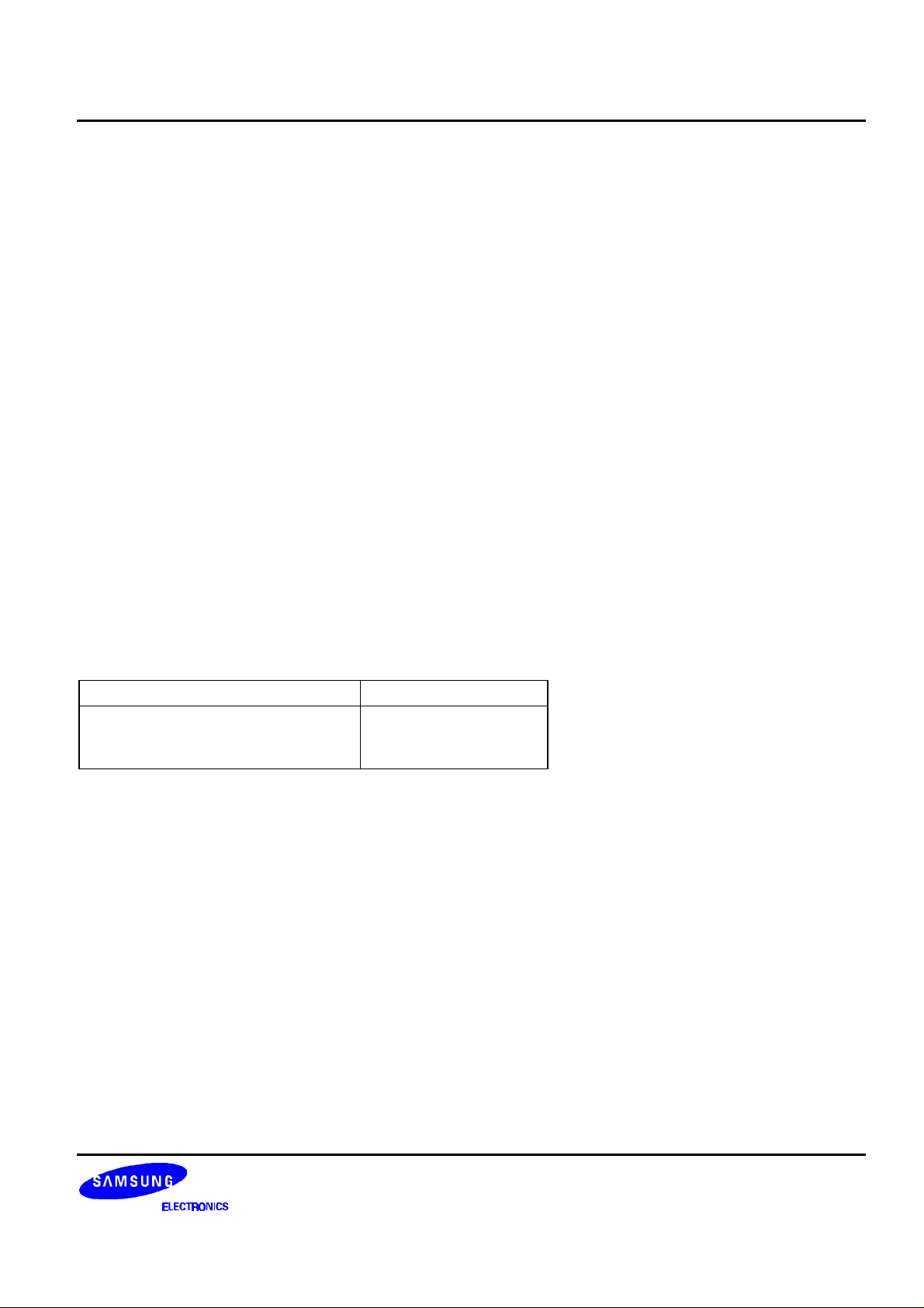
The S6A0065 is a LCD driver IC which is fabricated by low power CMOS technology. Basically this IC consists of
20 x 2 bit bi-directional shift register, 20 x 2 bit data latch and 20 x 2 bit driver. (refer to Fig 1) This IC can be
used as common or segment driver.
FUNCTION
• Dot matrix LCD driver with 40 channel output.
• Selects function to use common/segment drivers simultaneously.
• Input / Output signal
- Output: 20 x 2 channel waveform for LCD driving
- Input: Serial display data and control signal from the controller LSI.
Bias voltage (V1-V6)
FEATURES
• Display driving bias: static - 1/5
• Power supply voltage: 2.7- 5.5V
• Supply voltage for display: 3.0 - 13.0V (V
• Interface
= VDD - VEE)
LCD
Driver (cascade connection) Controller
Other S6A0065, S6A2067
S6A0069
S6A0070
S6A0073
• CMOS Process
• 64QFP or bare chip available
1
S6A0065 40 CH SEGMENT/COMMON DRIVER FOR DOT MATRIX LCD
BLOCK DIAGRAM
CL
CL
Part 1
SC
SC
SC
1
V
1
V
2
V
3
V
4
LCD DRIVER
SC
2
20
19
V
1
V
2
SC
Data Latch (20 bits)
Bidirectional
Shift Register (20 bits)
M
1
2
SW
CONTR
Logic
FCS DL
1
SHL
DR
1
1
DL
Shift Register (20 bits)
2
Part 2
SC
SC
22
21
39
LCD DRIVER
Data Latch (20 bits)
Bidirectional
SHL
SC
2
40
V
5
V
6
V
DD
V
SS
V
EE
DR
2
Figure 1. S6A0065 Functional Block Diagram
2
40 CH SEGMENT/COMMON DRIVER FOR DOT MATRIX LCD S6A0065
SC29
SC28
SC27
SC26
SC25
SC24
SC23
SC22
SC21
SC20
SC19
SC18
SC17
SC16
SC15
SC14
SC13
SC12
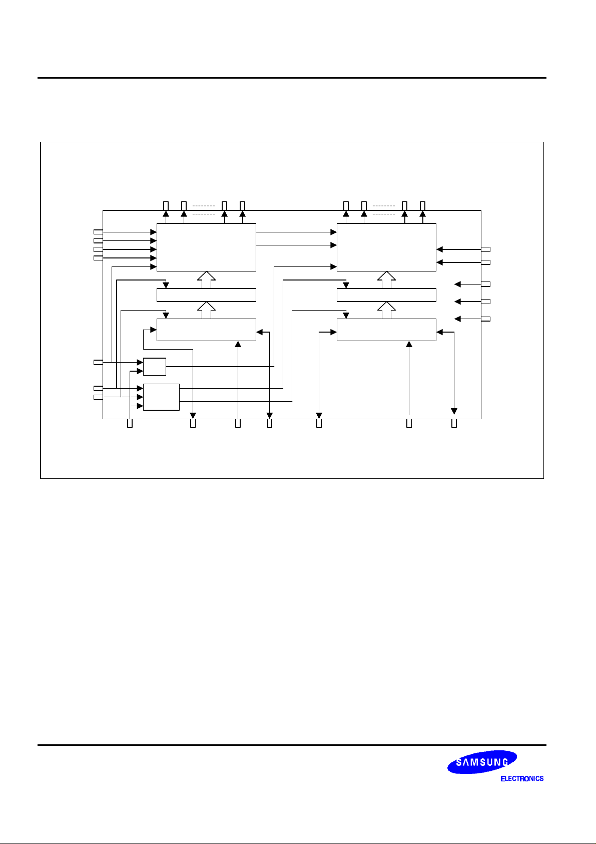
PIN CONFIGURATION
SC40
SC39
SC38
SC37
SC36
SC35
SC30
SC31
SC32
SC33
SC34
V6V5V4V3V2V1FCS
SHL2
SHL1MNC
DR2
DL2
DR1
49484746454443424140393837363534333231
50
51
52
53
54
55
S6A0065
56
57
58
59
60
1234567891011121314151617
Figure 2. 60 QFP Top View
DL1
GND(VSS)
CL2
CL1
VEE
30
29
28
27
26
25
24
23
22
21
20
19
SC1
SC2
SC3
SC4
SC5
SC6
V
DD
SC7
SC8
SC11
SC10
SC9
18
3
S6A0065 40 CH SEGMENT/COMMON DRIVER FOR DOT MATRIX LCD
2345678
9
101112131415161718
19
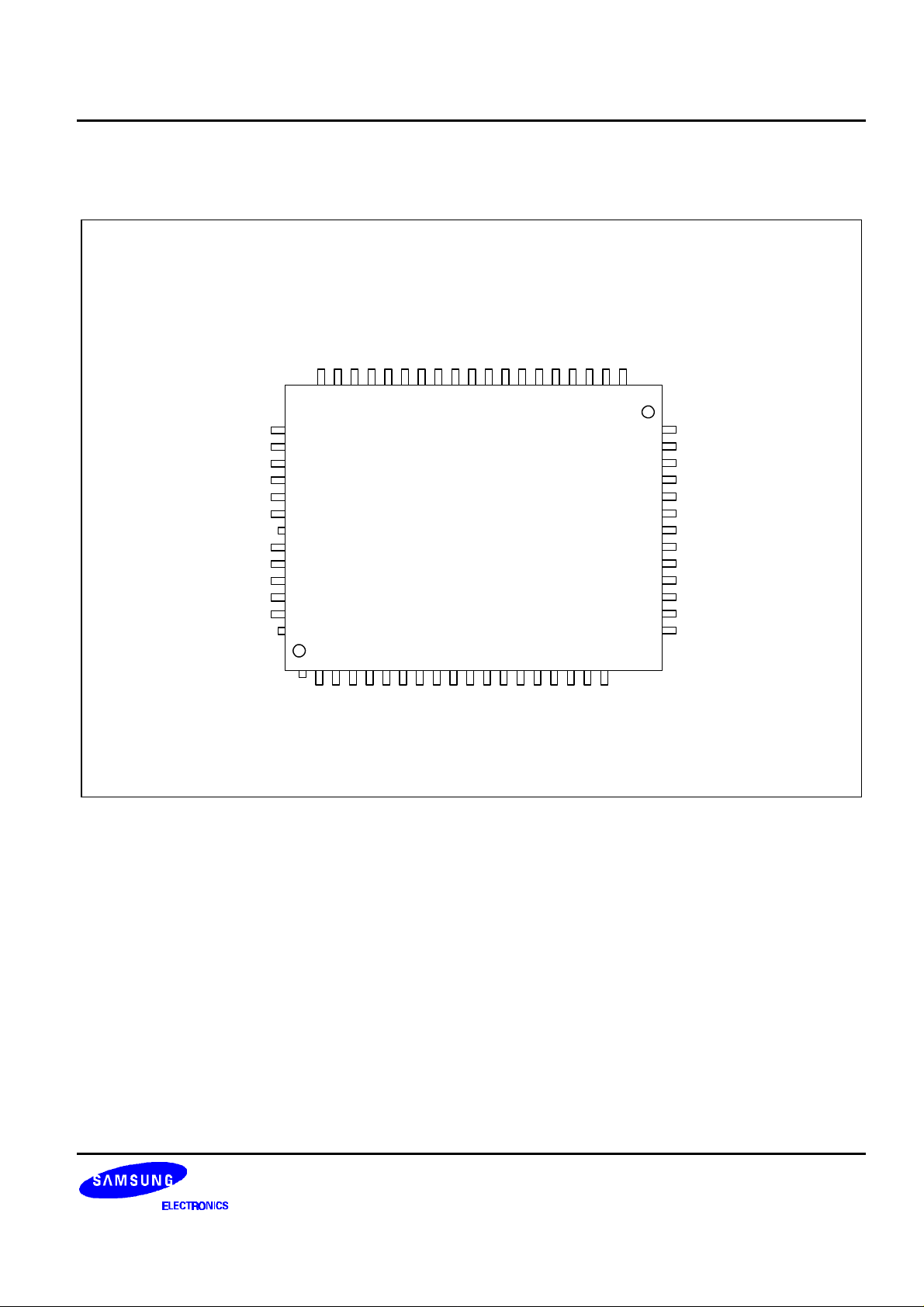
PAD DIAGRAM
4746454443424140393837363534333231
NOTE:
48
49
50
51
52
53
54
55
56
57
58
59
1
(0,0) is center in the chip.
S6A0065
Y
(0, 0)
Chip size: 2700
Pad size: 100
Unit: µm
30
29
28
27
26
25
X
2190
×
×
100
24
23
22
21
20
4

40 CH SEGMENT/COMMON DRIVER FOR DOT MATRIX LCD S6A0065
PAD CENTER COORDINATES
Unit: um
PAD PAD COORDINATE PAD PAD COORDINATE
NUMBER NAME X Y NUMBER NAME X Y
1 VEE -1120.2 -642.5 31 SC28 1117.5 865.2
2 CL1 -1062.5 -865.2 32 SC27 992.5 865.2
3 CL2 -937.5 -865.2 33 SC26 867.5 865.2
4 VSS -812.5 -865.2 34 SC25 742.5 865.2
5 DL1 -687.5 -865.2 35 SC24 617.5 865.2
6 DR1 -562.5 -865.2 36 SC23 492.5 865.2
7 DL2 -437.5 -865.2 37 SC22 367.5 865.2
8 DR2 -312.5 -865.2 38 SC21 242.5 865.2
9 M -187.5 -865.2 39 SC20 117.5 865.2
10 SHL1 -62.5 -865.2 40 SC19 -7.5 865.2
11 SHL2 62.5 -865.2 41 SC18 -132.5 865.2
12 FCS 187.5 -865.2 42 SC17 -257.5 865.2
13 V1 332.5 -865.2 43 SC16 -382.5 865.2
14 V2 457.5 -865.2 44 SC15 -507.5 865.2
15 V3 582.5 -865.2 45 SC14 -632.5 865.2
16 V4 707.5 -865.2 46 SC13 -757.5 865.2
17 V5 832.5 -865.2 47 SC12 -882.5 865.2
18 V6 957.5 -865.2 48 SC9 -1120.2 857.2
19 SC40 1082.5 -865.2 49 SC10 -1120.2 732.5
20 SC39 1120.2 -627.5 50 SC11 -1120.2 607.5
21 SC38 1120.2 -502.5 51 SC8 -1120.2 482.5
22 SC37 1120.2 -377.5 52 SC7 -1120.2 357.5
23 SC36 1120.2 -252.5 53 VDD -1120.2 232.5
24 SC35 1120.2 -127.5 54 SC6 -1120.2 107.5
25 SC30 1120.2 -2.5 55 SC5 -1120.2 -17.5
26 SC31 1120.2 122.5 56 SC4 -1120.2 -142.5
27 SC32 1120.2 247.5 57 SC3 -1120.2 -267.5
28 SC33 1120.2 372.5 58 SC2 -1120.2 -392.5
29 SC34 1120.2 497.5 59 SC1 -1120.2 -517.5
30 SC29 1120.2 622.5
5

S6A0065 40 CH SEGMENT/COMMON DRIVER FOR DOT MATRIX LCD
PIN DESCRIPTION
Pin (No.) I/O Name Description Interface
VDD(24)
Operating Voltage For logical circuit (2.7 - 5.5V) Power
GND(34) Power 0V (GND) Supply
VEE(31)
V1, V2
Negative Supply Voltage For LCD driver circuit
I Bias Voltage Bias voltage level for LCD drive (select level) Power
(44,45)
SC1 - SC
V3, V4
20
O LCD driver LCD driver output LCD
I Part 1 Bias Voltage Bias voltage level for LCD drive (non-select level)
Power
(46, 47)
SHL1(41)
DL1, DR1
(35, 36)
SC
21- SC40
V5, V6
I Data interface Selection of the shift direction of Part 1 shift
register
SHL1 DL1 DR1
VDD
VSS
out in
in out
I/O Data input/output of Part 1 shift register Controller or
O LCD driver LCD driver output
I Part 2 Bias Voltage Bias voltage level for LCD drive (non-select level)
VDD or V
S6A0065
Power
(48, 49)
SHL2(42)
I Data interface Selection of the shift direction of Part 2 shift
DL2,DR2
I/O Data input/output of Part 2 shift register Controller or
(37, 38)
M (40) I Alternated signal for LCD
driver output
CL1,CL2
I Data shift /latch clock
(32,33)
register
SHL2 DL2 DR2
VDD
VSS
out in
in out
Controller
PART FCS M polarttyCL2
V
1
V
V
2
V
CL1
latch clock shift clock
SS
DD
SS
latch clock shift clock
DD
M
M
VDD or V
S6A0065
SS
SS
FCS(43) I Mode selection Shift/latch clock of display data and polarity of M
signal are changed by FCS signal.
By setting FCS to VDD level, user can select the
function that use Part 1 as segment driver and
Part 2 as common driver simultaneously.
NC(39) No connection pin NC
6

40 CH SEGMENT/COMMON DRIVER FOR DOT MATRIX LCD S6A0065
MAXIMUM ABSOLUTE LIMIT
(Ta = 25°C)
Characteristic Symbol Value Unit
Operating Voltage
Driver Supply Voltage
Input Voltage 1
Input Voltage 2 (V1 - V6) V
Operating Temperature
Storage Temperature
VDD
V
LCD
V
IN1
IN2
T
OPR
T
SRG
*
Voltage greater than above may damage the circuit
*
VEE: connect a protection resistor (220Ω ± 5%)
ELECTRICAL CHARACTERISTICS
DC Characteristics
Characteristic Symbol
Operating Current *
Supply Current *
Input High Voltage
Input Low Voltage
Input Leakage
Current
Output High
Voltage
Output Low Voltage
Voltage
Descending
Leakage Current
(V
= 2.7 - 5.5V, VDD-VEE = 3 - 13V, VSS = 0V, Ta = -30 - +85°C)
DD
Test condition
IDD f
I
f
EE
V
IH
V
IL
I
VIN = 0-VDD
LKG
V
I
OH
V
l
OL
V
I
D1
= 400kHz
CL2
= 1kHz
CL1
0
= -0.4mA VDD-0.4
OH
= +0.4mA
OL
= 0.1mA for one of
ON
SC1-SC40
V
D2
I
= 0.05mA for each
ON
SC1-SC40
I
VIN = VDD V
V
(Output SC1-SC40 : floating)
- 0.3 to + 7.0 V
VDD - 15.0 to VDD + 0.3
- 0.3 to VDD + 0.3
VDD + 0.3 to VEE - 0.3
- 30 to + 85
- 55 to + 125
Min
Max Unit Applicable pin
- 1 mA -
- 10
-
0.7V
DD
V
0.3V
DD
DD
-5 5
- DL1, DL2,
- 0.4 V
- 1.1 V(V1-V6)-
- 1.5
EE
-10 10
V
V
V
°C
°C
µA
V CL1, CL2, DL1,
DL2
DR1, DR2,
SHL1, SHL2
µA
M, FCS
DR1, DR2
SC(SC1-SC40)
µA
V1-V6
7

S6A0065 40 CH SEGMENT/COMMON DRIVER FOR DOT MATRIX LCD
AC Characteristics
Characteristic Symbol Test condition Min Max Unit Applicable pin
Data Shift Frequency
Clock High Level Width
Clock Low Level Width
Clock Set-up Time
Clock Rise/Fall Time
Data Set-up Time
(VDD = 2.7 to 5.5V, VDD-VEE = 3 to 13V, VSS = 0V, Ta = -30 to +85 °C)
fCL
t
WCKH
t
WCKL
tSL
tLS
tR/tF
tSU
from CL2 to CL1 500 - ns
from CL1 to CL2 500 - CL1, CL2
- - 400 kHz CL2
- 800 - CL1, CL2
- 800 - CL2
- - 200
- 300 - DL1, DL2, DR1,
DR2, FLM
Data Hold Time
Data Delay Time
tDH
- 300 -
tD CL = 15pF
- 500 DL1, DL2,
DR1, DR2
* Input/Output current is excluded; When input is at the intermediate level with CMOS, excessive current flows
through the input circuit to the power supply, To avoid this, input level must be fixed at "H" or "L".
8

40 CH SEGMENT/COMMON DRIVER FOR DOT MATRIX LCD S6A0065
TIMING CHARACTERISTICS
CL2
VIH
VIL
tR tWCKH tF
Data in
(DL1,DL2)
(DR1, DR2)
VIH
VIL
tD
Data out
(DL1,DL2)
VOH
VOL
(DR1, DR2)
CL1
FLM
FUNCTIONAL DESCRIPTION
tWCKL
tDH
tSU
VIH
Figure 3. AC characteristics
VIL
VIL
VIH
tSU
VIL
VIH
tSL
tLS
tLS
tWCKH
tR
tF
1) To Drive Segment Type
When the FCS is connected to VSS, S6A0065 (SC1-SC40) is operated as segment driver.(refer to Fig 4)
M
Latch
CL1
Shift
CL2
DL1/DR1
DL2/DR2
Output of
Latch (SC)
SC2
SC1 SC39 SC40
SC1 - SC40
Figure 4. Segment Data Waveform
9

S6A0065 40 CH SEGMENT/COMMON DRIVER FOR DOT MATRIX LCD
2) To Drive Common Type
When the FCS is connected to VDD, only part2 (SC21-SC40) of S6A0065 is operated as common driver. (refer to
Fig 5).
DL2/DR2
M
Latch
CL1
Shift
CL2
Output of
Latch (SC)
Figure 5. Common Data Waveforms
LCD OUTPUT WAVEFORMS
FCS
Output of
Latch (DATA)
M
Part 1
(SC1 - SC20)
(SC21 - SC40)
Part 2
V1
V2
SC21 - SC40
V2
V4
V3
V1
V5
V6
V1
V1
V2
V4
V3
V2
V5
V6
*1
Figure 6. Output Waveforms
*1: To use for same function of part 1 and part 2, V3 and V5, V4 and V6 of power supply for LCD drive are short
circuited respectively.
10

40 CH SEGMENT/COMMON DRIVER FOR DOT MATRIX LCD S6A0065
APPLICATION CIRCUIT
1) Segment Driver
S6A0069
(Controller)
M
CLK2 CLK1 D
COM16
2) Common Driver
COM1
~
common signal
SHL1
SHL2
FCS
DL1
DR1
DL2
SC1 - SC
S6A0065
(seg driver)
CL1CL2 M
40
DR2
LCD
segment signal
SHL1
SHL2
FCS
DL1
DR1
DL2
SC1 - SC
S6A0065
(seg driver)
CL1CL2 M
40
DR2
open
FCS
SHL1
SHL2
CL1
CL2
CL1
CL2
Controller LCD
FLM
DL1
DR1
S6A0065
(Com Driver)
SC
1
-SC
40
Common
Signal
Segment Signal
DL2
SC1-SC
40
S6A0065
(Seg Driver)
11
SC1-SC
40
S6A0065
(Seg Driver)

S6A0065 40 CH SEGMENT/COMMON DRIVER FOR DOT MATRIX LCD
3) Segment / Common Driver
common
signal
LCD
Controller
M
CL1 CL2
FLM
VDD
SC21 - SC
D
DL1
DL2
40
SC1 - SC
S6A0065
(seg/com
driver)
FCS
DR1
SHL1
SHL2
CL1 CL2 M
segment signal
20
FCS
SHL1
SHL2
DL1
DR1
DL2
SC1 - SC
40
S6A0065
(seg driver)
CL1CL2 M
DR2
open
12
 Loading...