

Page 1
MT90863
3V Rate Conversion Digital Switch
Advance Information
Features
• 2,048 × 512 and 512 x 512 switching among
backplane and local streams
• Rate conversion between 2.048, 4.096 and
8.192Mb/s
• Optioal sub-rate switch configuration for
2.048 Mb/s streams
• Per-channel variable or constant throughput
delay
• Compatible to HMVIP and H.100 specifications
• Automatic frame offset delay measurement
• Per-stream frame delay offset programming
• Per-channel message mode
• Per-channel direction control
• Per-channel high impedance output control
• Non-multiplexed microprocessor interface
• Connection memory block programming
• 3.3V local I/O with 5V tolerant inputs and
TTL-compatible outputs
• IEEE-1149.1 (JTAG) Test Port
Applications
• Medium and large switching platforms
• CTI application
• Voice/data multiplexer
• Support ST-BUS, HMVIP and H.100 interfaces
DS5034 ISSUE 3 March 1999
Ordering Information
MT90863AL1 128 Pin MQFP
MT90863AG1 144 Pin BGA
-40 to +85 C
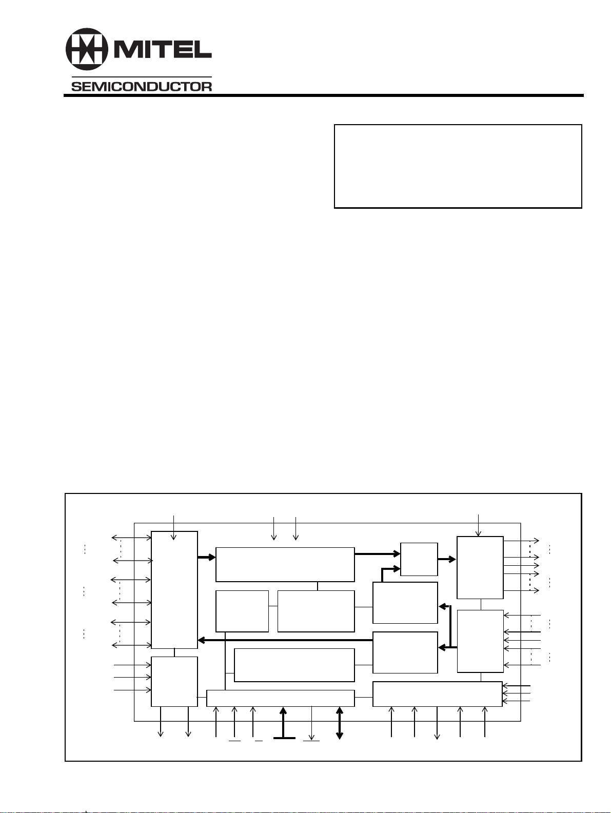
Description
The MT90863 Rate Conversion Switch provides
switching capacities of 2,048 × 512 channels
between backplane and local streams, and 512 x
512 channels for local streams. The connected serial
inputs and outputs may have 32, 64 and 128 64kb/s
channels per frame with data rates of 2.048Mb/s,
4.096Mb/s and 8.192Mb/s respectively.
The MT90863 also offers a sub-rate switching
configuration which allows 2-bit wide 16kb/s data
channels to be switched within the device.
The device has features (such as: message mode;
input and output offset delay; direction control; and,
high impedance output control) that are
programmable on per-stream or per-channel basis.
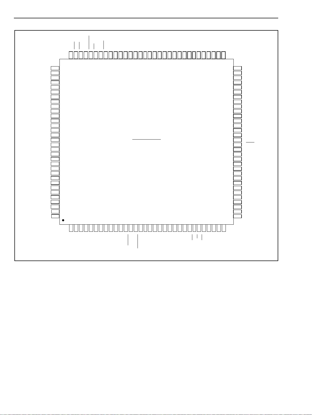
STio0/
FEi0
STio15/
FEi15
STio16/
FEi16
STio23/
FEi23
STio24
STio31
C16i
F0i
C4i/C8i
ODE
Backplane
Interface
S/P
&
P/S
Converter
Timing
Unit
F0o DS CS R/W A7-A0 DTA D15-D0
C4o
Multiple Buffer
(2,048 channels)
Internal
Registers
Microprocessor Interface
V
V
SS
DD
Data Memory
Local
Connection
Memory High/Low
(512 locations)
Backplane
Connection
Memory
(2,048 locations)
Figure 1 - Functional Block Diagram
Output
Mux
Multiple Buffer
Data Memory
(512 channels)
Multiple Buffer
Data Memory
(512 channels)
Test Port
TDI TDO
TMS
Interface
Converter
Interface
Converter
TCK
ODE
Local
P/S
Local
S/P
TRST
STo0
STo11
STo12
STo13
STo15
STi0
STi11
STi12
STi13
STi15
RESET
IC1
IC2
1
Page 2
MT90863 Advance Information
VDD
STo0
STo1
STo2
STo3
STo4
STo5
STo6
STo7
VSS
VSS
C4o
F0o
VSS
F0i
C4i/C8i
VSS
C16i
VSS
STo14
ST015
STo12
STo13
STo10
STo11
STo8
STo9
VDD
ODE
VSS
STi14
STi15
VDD
STio0/FEi0
STio1/FEi1
STio2/FEi2
STio3/FEi3
STio4/FEi4
STio5/FEi5
STio6/FEi6
STio7/FEi7
VSS
VDD
STio8/FEi8
STio9/FEi9
STio10/FEi10
STio11/FEi11
STio12/FEi12
STio13/FEi13
STio14/FEi14
STio15/FEi15
VSS
VDD
STio16/FEi16
STio17/FEi17
STio18/FEi18
STio19/FEi19
STio20/FEi20
STio21/FEi21
STio22/FEi22
STio23/FEi23
VSS
VDD
STio24
97
99
101
103
105
107
109
111
113
115
117
119
121
123
125
127
79858789 7173757793 6791 69 6583 8195
128 Pin PQFP
171197252321193 295273113 151
63
STi12
STi11
STi13
61
STi10
STi9
59
STi8
STi7
57
STi6
STi5
55
STi4
STi3
53
STi2
STi1
51
STi0
VDD
49
VSS
DTA
47
D15
D14
45
D13
D12
43
D11
D10
41
D9
D8
39
VSS
D7
37
D6
D5
35
D4
D3
33
D2
STio25
STio26
STio27
STio28
STio29
STio30
VSS
STio31
TMS
TDI
TDO
TCK
IC1
TRST
IC2
VSS
RESET
A0
A4
A3
A2
A1
Figure 2 - MQFP Pin Connections
A5
A6
A7
DS
D1
D0
CS
R/W
VSS
VDD
2
Page 3
Advance Information MT90863
1
A
B
C
D
E
F
G
H
J
K
L
M
N
12345678910111213
STio24
STio26
STio25
STio29
TMS
TDI
TDOTCK
TRST IC1RESET
A0
VSS
A1 A2 A3
A4A5 A6
A7
DS
R/WCS
D0D1D2D3D4
STio17
STio19
STio22
STio16
STio18
STio20
STio23
STio21
STio27STio28
STio30STio31
VSS
VSS
VDD
IC2
VSS
VDD
VSS
VDD
D5D6D7
VSS VSS
D8D9D10
TOP VIEW
D11
D12
D14D13
STio11
STio14STio15
STio10
STio13
STio12
D15
DTA STi0
STio9
VDD
STi1
STio6
STio8
STio5
STio7
VSSVSSVDD
VDD
VDDVSSVDDVSSVDDVSS VSS
VDD
VSS
VDD
VSS
VSS
VSSVDDVSSVDDVSSVDD VDD
STi6
STi8
STi7
STi4
STi2 STi3
STio3STio4
STio1STio2
C4o
STio0
C16iF0i
STo14
VSS
VDD
STo4 STo5STo6
VSS
VDD
STi12
STi15 ODE
STi13 STi14
STi10
STi5
STi9
F0o
C4i/C8i
STo15
STo13
STo11STo12
STo9STo10
STo7STo8
STo2STo3
STo0STo1
STi11
1 - A1 corner is identified by metallized markings.
Figure 3 - BGA Pin Connections
Pin Description
128 MQFP
Pin#
30,50,67,
79,97,107,
117,127
8,17,29,39,
49,68,78,8
8,90,93,96,
106,
116,126
89 D12 C16i Master Clock (5V Tolerant Input): Serial clock for shifting data in/out
91 D11 F0i Master Frame Pulse (5V T olerant Input): In ST-BUS mode, this input
144 BGA
Pin#
C5,C9,D5,D7,
D9,E10,F4,G10
,G11,H4,
K3,K4,K6,K8
K10,K11,L8
C6,C10,D4,D6,
D8,D10,E3,E4,
F10,F11,G2,
G4,H10,J4,
J10,J11,K5
K7,K9,L3,L7
Name Description
V
DD
V
ss
+3.3 Volt Power Supply
Ground
on the serial streams. This pin accepts a 16.384 MHz clock.
accepts a 61ns wide negative frame pulse. In CT Bus mode, it accepts
a 122ns wide negative frame pulse. In HMVIP mode, it accepts a
244ns wide negative frame pulse.
3
Page 4

MT90863 Advance Information
Pin Description (continued)
128 MQFP
Pin#
92 B13 C4i/C8i HMVIP/CT Bus Clock (5V Tolerant Input): When HMVIP mode is
94 A13 F0o Frame Pulse (5V Tolerant Output): A 244ns wide negative frame
95 C12 C4o C4 Clock (5V Tolerant Output): A 4.096MHz clock that is phase
98-105,
108-115
118-125 B6, A5, B5, A4,
144 BGA
Pin#
C11, B12, B11,
A12, A11, B10,
A10, B9, A9,
C8, B8, A8, C7,
B7, A7, A6,
B4, C4, A3, B3
Name Description
enabled, this pin accepts a 4.096MHz clock for HMVIP frame pulse
alignment. When CT Bus mode is enabled, it accepts a 8.192MHz
clock for CT frame pulse alignment.
pulse that is phase locked to the master frame pulse (F0i).
locked to the master clock (C16i).
STio0 - 15
FEi0 - 15
STio16 - 23
FEi16 - 23
Serial Input Streams 0 to 15 / Frame Evaluation Inputs 0 to 15 (5V
Tolerant I/O). In 2Mb/s and HMVIP modes, these pins accept serial
TDM data streams at 2.048 Mb/s with 32 channels per stream. In 4Mb/
s or 8Mb/s mode, these pins accept serial TDM data streams at 4.096
or 8.192 Mb/s with 64 or 128 channels per stream respectively. In
Frame Evaluation Mode (FEM), they are frame evaluation inputs.
Serial Input Streams 16 to 23 (5V Tolerant I/O). In 2Mb/s or 4Mb/s
mode, these pins accept serial TDM data streams at 2.048 or 4.096
Mb/s with 32 or 64 channels per stream respectively. In HMVIP mode,
these pins have a data rate of 8.192Mb/s with 128 channels per
stream. In Frame Evaluation Mode (FEM), they are frame evaluation
inputs.
128,
1-7
9 C1 TMS Test Mode Select (3.3V Input with internal pull-up): JTAG signal
10 D1 TDI Test Serial Data In (3.3V Input with internal pull-up): JTAG serial
11 E2 TDO T est Serial Data Out (3.3V Output):JTAG serial data is output on this
12 E1 TCK Test Clock (5V Tolerant Input): Provides the clock to the JTAG test
13 F2 TRST Test Reset (3.3 V Input with internal pull-up): Asynchronously
14 F3 IC1 Internal Connection 1 (3.3V Input with internal pull-down):
15 F1 RESET Device Reset (5V Tolerant Input): This input (active LOW) puts the
A2, B2, A1, C3,
C2, B1, D3, D2
STio24 - 31 Serial Input Streams 24 to 31 (5V Tolerant I/O). These pins are only
used for 2Mb/s or 4Mb/s mode. They accept serial TDM data streams
at 2.048 or 4.096 Mb/s with 32 or 64 channels per stream respectively.
that controls the state transitions of the TAP controller.
test instructions and data are shifted in on this pin.
pin on the falling edge of TCK. This pin is held in a high impedance
state when JTAG scan is not enabled.
logic.
initializes the JTAG TAP controller by putting it in the Test-Logic-Reset
state. This pin should be pulsed low on power-up, or held low
continuously, to ensure that the MT90863 is in the normal operation
mode.
Connect to VSS for normal operation.
MT90863 in its reset state. This clears the device’s internal counters
and registers. It also brings microport data bus STio0 - 31 and STo0 15 to a high impedance state.
16 G3 IC2 Internal Connection 2 (3.3V Input):
Connect to VSS for normal operation.
4
Page 5

Advance Information MT90863
Pin Description (continued)
128 MQFP
Pin#
18-25 G1, H1, H2,
26 K2 DS Data Strobe (5V Tolerant Input): This active low input works in
27 L2 R/W Read/Write (5V Tolerant Input): This input controls the direction of
28 L1 CS Chip Select (5V Tolerant Input): Active low input used by a
31-38,
40-47
48 N7 DTA Data Transf er Acknowledgment (5V Tolerant Three-state Output):
51-54 N8, M8, N9,
144 BGA
Pin#
H3, J2, J1,J3,
K1
M1, N1, M2, N2,
M3, L4, N3, L5,
M4, N4, M5,
L6, M6, N5, N6,
M7,
N10
Name Description
A0 - A7 Address 0 - 7 (5V Tolerant Input): These lines provide the A0 to A7
address lines to the internal memories.
conjunction with CS to enable the read and write operations.
the data bus lines (D0-D15) during a microprocessor access.
microprocessor to activate the microprocessor port.
D0 - 7,
D8 - D15
STi0 - 3 Serial Input Streams 0 to 3 (5V Tolerant Inputs): In 2Mb/s or
Data Bus 0 -15 (5V T olerant I/O): These pins f orm the 16-bit data bus
of the microprocessor port.
This active low output indicates that a data bus tr ansfer is complete. A
pull-up resistor is required to hold a HIGH level when the pin is tristated.
Subrate Switching mode, these inputs accept data rates of 2.048 Mb/s
with 32 channels per stream. In 8Mb/s mode, these inputs accept data
rates of 8.192 Mb/s with 128 channels per stream.
55-62 M9, N11, L9,
M10, L10, N12,
M11, N13
63 L11 STi12 Serial Input Streams 12 (5V Tolerant Input): In 2Mb/s mode, this
64-66 M12, M13, L12 STi13 - 15 Serial Input Streams 13 to 15 (5V Tolerant Inputs): In 2Mb/s mode,
69 L13 ODE Output Drive Enable (5V Tolerant Input): This is the output enable
70-73 K13, K12, J13,
J12
74-77,
80-83
H11, H13, H12,
G13, G12, F13,
F12, E13
STi4 - 11 Serial Input Streams 4 to 11 (5V Tolerant Inputs): In 2Mb/s or Sub-
rate Switching mode, these inputs accept data rates of 2.048Mb/s
with 32 channels per stream.
input accepts data rate of 2.048Mb/s with 32 channels per stream
respectively. In Sub-rate Switching mode, this pin accepts 2.048Mb/s
with 128 channels per stream for Sub-rate switching application.
these inputs accept a data rate of 2.048Mb/s with 32 channels per
stream.
control for the STo0 to ST o15 serial outputs and STio0 to STio31 serial
bidirectional outputs.
STo0 - 3 Serial Output Streams 0 to 3 (5V T olerant Three-state Outputs): In
2Mb/s or Sub-rate Switching mode, these outputs have data rates of
2.048 Mb/s with 32 channels per stream respectively. In 8Mb/s mode,
these outputs have data rates of 8.192 Mb/s with 128 channels per
stream
STo4 - 7,
STo8 - 11
Serial Output Streams 4 to 11 (5V Tolerant Three-state Outputs):
In 2Mb/s or Sub-rate Switching mode, these outputs have data r ates of
2.048Mb/s with 32 channels per stream
5
Page 6
MT90863 Advance Information
Pin Description (continued)
128 MQFP
Pin#
84 E12 STo12 Serial Output Streams 12 (5V Tolerant Three-state Output): In
85-87 D13, E11, C13 STo13 - 15 Serial Output Streams 13 to 15 (5V Tolerant Three-state Outputs):
Device Overview
The Rate conversion Switch (MT90863) can switch
up to 2,048 × 512 channels while also providing a
rate conversion capability. It is designed to switch 64
kb/s PCM or N X 64 kb/s data between the
backplane and local interfaces. When the device is in
the sub-rate switching mode, 2-bit wide 16 kb/s data
channels can be switched within the device. The
device maintains frame integrity in data applications
and minimum throughput delay for voice application
on a per channel basis.
144 BGA
Pin#
Name Description
2Mb/s mode, this output has data rate of 2.048Mb/s with 32 channels
per stream. In Sub-rate Switching mode, this pin has data rate of
2.048Mb/s with 128 channels per stream for Sub-rate switching
application.
In 2Mb/s mode, these outputs have a data rate of 2.048Mb/s with 32
channels per stream.
Frame Alignment Timing
The Device Mode Selection (DMS) register allows
users to select three different frame alignment timing
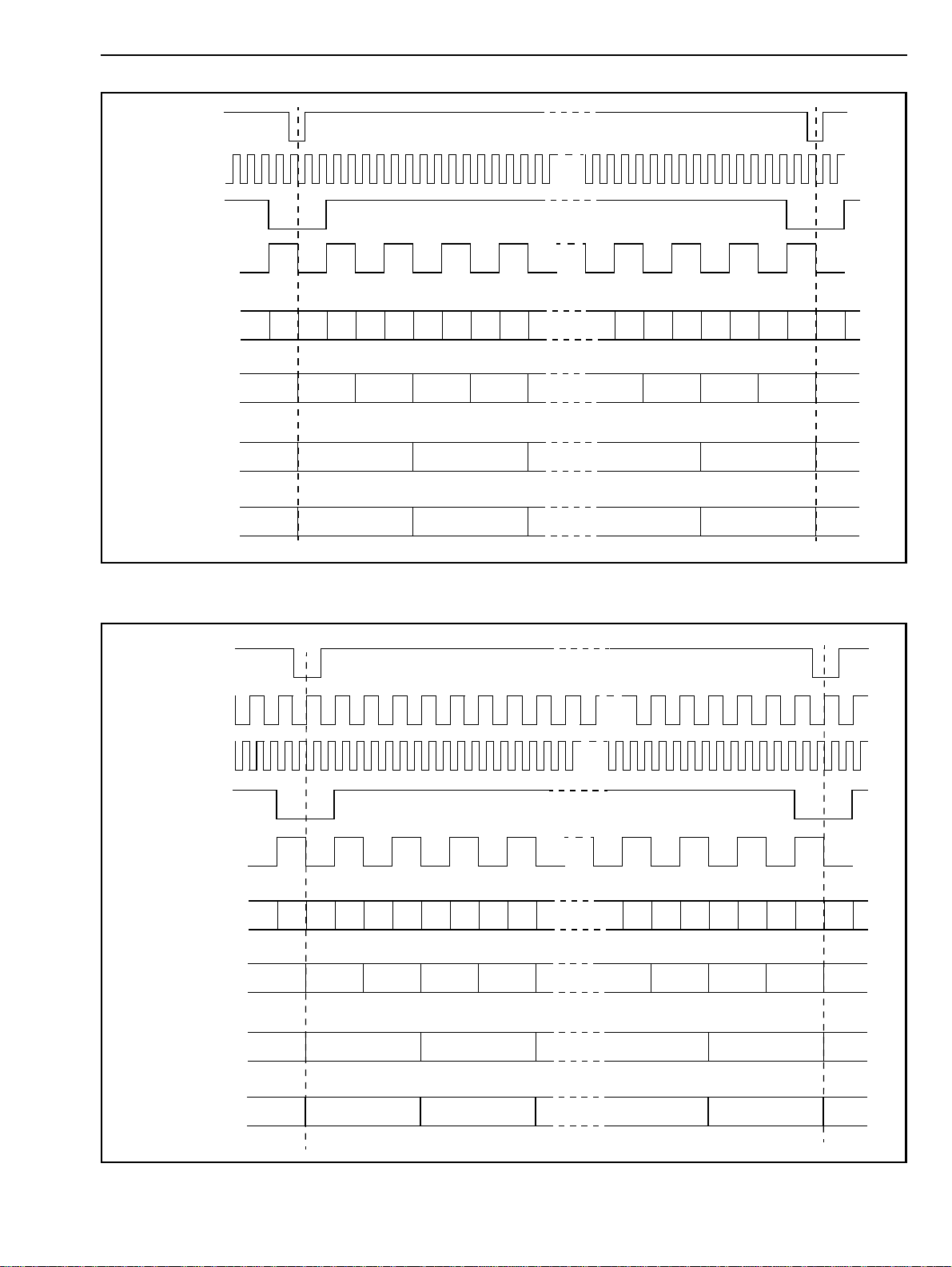
modes. In ST-BUS modes, the master clock (C16i) is
always at 16.384 MHz. The frame pulse (F0i) input
accepts a negative frame pulse at 8kHz. The frame
pulse goes low at the frame boundary for 61ns. The
frame pulse output F0o provides a 244ns wide
negative frame pulse and the C4o output provides a
4.094MHz clock. These two signals are used to
support local switching applications. See Figure 4 for
the ST-BUS timings.
The backplane interface can operate at 2.048, 4.096
or 8.192 Mb/s, arranged in 125µs wide frames that
contain 32, 64 or 128 channels, respectively. A builtin rate conversion circuit allows users to interface
between backplane interface and the local interface
which operates at 2.048 Mb/s or 8.192 Mb/s.
By using Mitel’s message mode capability, the
microprocessor can access input and output timeslots on a per channel basis. This feature is useful
for transferring control and status information for
external circuits or other ST-Bus devices.
The frame offset calibration function allows users to
measure the frame offset delay for streams STio0 to
STio23. The offset calibration is activated by a frame
evaluation bit in the frame evaluation register. The
evaluation result is stored in the frame evaluation
registers and can be used to programme the input
offset delay for individual streams using internal
frame input offset registers.
Functional Description
A functional Block Diagram of the MT90863 is shown
in Figure 1. One end of the MT90863 is used to
interface with backplane applications, such as
HMVIP or H.100 environments, while the other end
supports the local switching environments.
In CT Bus mode, the C4i/C8i pin accepts 8.192MHz
clock for the CT Bus frame pulse alignment. The F0i
is the CT bus frame pulse input. The CT frame pulse
goes low at the frame boundary for 122ns. See
Figure 5 for the CT Bus timing.
In HMVIP mode, the C4i/C8i pin accepts 4.096MHz
clock for the HMVIP frame pulse alignment. The F0i
is the HMVIP frame pulse input. The HMVIP frame
pulse goes low at the frame boundary for 244ns. See
Figure 6 for the HMVIP timing.
Table 1 describes the input timing requirements for
ST-BUS, CT Bus and HMVIP modes.
Switching Configuration
The device has four operation modes for the
backplane interface and three operation modes for
the local interface. These modes can be
programmed via the Device Mode Selection (DMS)
register. Mode selections between the backplane
and local interfaces are independent. See Table 2
and Table 3 for the selection of various operation
modes via the programming of the DMS register.
6
Page 7
Advance Information MT90863
F0i
C16i
F0o
C4o
STio 0 - 15
STi/STo 0 - 3
(8Mb/s mode)
STio 0 - 31
(4Mb/s mode)
STio 0 - 31
STi/STo 0 - 15
(2Mb/s mode)
STi12/STo12
(Sub-rate
Switching)
F0i
(CT_FRAME)
C4i/C8i
(8.192MHz)
C16i
Channel 0
72345610
0
1
Channel 0
0
0
01 0
7564
Channel 0
76
Channel 0
Channel 127
Channel 63
Channel 31
1
Channel 127
Figure 4 - ST-BUS Timing for 2, 4 and 8 Mb/s Data Streams
2345610
12307
0
7
7
Bit 101
F0o
C4o
STio 0 - 15
STi/STo 0 - 3
(8Mb/s mode)
STio 0 - 31
(4Mb/s mode)
STio 0 - 31
STi/STo 0 - 15
(2Mb/s mode)
STi12/STo12
(Sub-rate
Switching)
Channel 0
72345610
0
1
Channel 0
0
0
01 0
7564
Channel 0
76
Channel 0
Channel 127
Channel 63
12307
Channel 31
1
Channel 127
Figure 5 - CT Bus Mode Timing for 2, 4 and 8 Mb/s Data Streams
2345610
0
7
7
Bit 101
7
Page 8
MT90863 Advance Information
F0i
(HMVIP Frame)
C4i/C8i
(4.096MHz)
C16i
F0o
C4o
STio 0 - 15
STi/STo 0 - 15
(2Mb/s mode)
STio 16 - 23
(8Mb/s mode)
Channel 0
0
0
1
76
Channel 0
72345610
Channel 31
1
Channel 127
0
2345610
7
7
Channel 0
STi12/STo12
(Sub-rate
Switching)
01 0
Figure 6- HMVIP Mode Timing for 2 and 8 Mb/s Data Streams
Backplane Interface
The backplane interface can be programmed to
accept data streams of 2Mb/s, 4Mb/s or 8Mb/s.
When 2Mb/s mode is enabled, STio0 to STio31 have
a data rate of 2.048Mb/s. When 4Mb/s mode is
enabled, STio0 to STio31 have a data rate of
4.096Mb/s. When 8Mb/s mode is enabled, STio0 to
STio15 have a data rate of 8.192Mb/s. When HMVIP
mode is enabled, STio0 to STio15 have a data rate
of 2.048Mb/s and STio16 to STio23 have a data rate
of 8.192Mb/s.
Table 2 describes the data rates and mode selection
for the backplane interface.
Local Interface
Three operation modes, 2Mb/s, 8Mb/s and Sub-rate
Switching mode, can be selected for the local
interface. When 2Mb/s mode is selected, STi0 to
STi15 and STo0 to STo15 have a 2.048Mb/s data
rate. When 8Mb/s mode is selected, STi0 to STi3
and STo0 to STo3 have an 8.192Mb/s data rate.
When Sub-rate Switching mode is selected, STi0 to
STi11 and STo0 to STo11 have 2.048Mb/s data with
64kb/s data channels and STi12 and STo12 have a
2.048Mb/s data rate with 16kb/s data channels.
Table 3 describes the data rates and mode selection
for the local interface.
Input Frame Offset Selection
Input frame offset selection allows the channel
alignment of individual backplane input streams, that
Channel 127
Bit 101
operate at 8.192Mb/s (STio0-23), to be shifted
against the input frame pulse (F0i). This feature
compensates for the variable path delays caused by
serial backplanes of variable length. Such delays can
be occur in large centralized and distributed
switching systems.
Each backplane input stream can have its own delay
offset value by programming the input delay offset
registers (DOS0 to DOS5). Possible adjustment can
range up to +4 master clock (C16i) periods forward
with resolution of half master clock period. See Table
10 and Table 11, and Figure 9, for frame input delay
offset programming.
Output Advance Offset Selection
The MT90863 allows users to advance individual
backplane output streams which operate at 8.192Mb/
s (STio0-23) by half a master clock (C16i) cycle. This
feature is useful in compensating for variable output
delays caused by various output loading conditions.
The frame output offset registers (FOR0 & FOR1)
control the output offset delays for each backplane
output stream via the OFn bit programming. Table 12
and Figure 10 detail frame output offset
programming.
Serial Input Frame Alignment Evaluation
The MT90863 provides the frame evaluation inputs,
FEi0 to FEi23, to determine different data input
delays with respect to the frame pulse F0i. By using
the frame evaluation input select bits (FE0 to FE4) of
8
Page 9

Advance Information MT90863
Timing Signals ST-BUS Mode CT Bus Mode HMVIP Mode
F0i Width 61ns 122ns 244ns
C4i/C8i Not Required 8.192MHz 4.096MHz
C16i 16.384MHz
F0o Width 244ns
C4o 4.096MHz
Table 1 - Timing Signals Requirements for Various Operation Modes
DMS Register Bits
Modes Backplane Interface Data Rate
BMS2 BMS1 BMS0
0 0 0 2Mb/s, ST-BUS Mode STio0 - 31 2.048 Mb/s
0 0 1 2Mb/s, CT Bus Mode STio0 - 31 2.048 Mb/s
0 1 0 4Mb/s, ST-BUS Mode STio0 - 31 4.096 Mb/s
0 1 1 4Mb/s, CT Bus Mode STio0 - 31 4.096 Mb/s
1 0 0 8Mb/s, ST-BUS Mode STio0 - 15 8.192 Mb/s
STio16 - 31 Not available
1 0 1 8Mb/s, CT Bus Mode STio0 - 15 8.192 Mb/s
STio16 - 31 Not available
1 1 0 HMVIP Mode STio0 - 15 2.048 Mb/s
STio16 - 23 8.192 Mb/s
STio24 - 31 Not available
Table 2 - . Mode Selection for Backplane interface
DMS Register Bits
Modes Local Interface Data Rate
LMS1 LMS0
0 0 2Mb/s Mode STi0 - 15 2.048 Mb/s
STo0 - 15 2.048 Mb/s
0 1 Sub-Rate
Switching
Mode
STi0 - 11 2.048 Mb/s
STi12 Sub-rate Switching Input Stream at 2.048 Mb/s
STi13 - 15 Not available
STo0 - 11 2.048 Mb/s
STo12 Sub-rate Switching Output Stream at 2.048Mb/s
STo13 - 15 Not available
1 0 8Mb/s Mode STi0 - 3 8.192 Mb/s
STi4 - 15 Not available
STo0 - 3 8.192 Mb/s
STo4 - 15 Not available
Table 3 - . Mode Selection for Local Interface
9
Page 10

MT90863 Advance Information
the frame alignment register (FAR), users can select
one of the twenty-four frame evaluation inputs for the
frame alignment measurement.
A measurement cycle is started by setting the start
frame evaluation (SFE) bit low for at least one frame.
Then the evaluation starts when the SFE bit in the
Internal Mode Selection (IMS) register is changed
from low to high. One frame later, the complete
frame evaluation (CFE) bit of the frame alignment
register changes from low to high to signal that a
valid offset measurement is ready to be read from
bits 0 to 9 of the FAR register. The SFE bit must be
set to zero before a new measurement cycle is
started.
The falling edge of the frame measurement signal
(FEi) is evaluated against the falling edge of the
frame pulse (F0i). Table 8 and Figure 8 describe the
frame alignment register.
Memory Block Programming
The MT90863 has two connection memories: the
backplane connection memory and the local
connection memory. The local connection memory is
partitioned into high and low parts. The IMS register
provides users with the capability of initializing the
local connection memory low and the backplane
connection memory in two frames. Bit 11 to bit 13 of
every backplane connection memory location will be
programmed with the pattern stored in bit 7 to bit 9 of
the IMS register. Bit 12 to 15 of every local
connection memory low location will be programmed
with the pattern stored in bits 3 to 6 of the IMS
register.
The block programming mode is enabled by setting
the memory block program (MBP) bit of the control
register high. When the block programming enable
(BPE) bit of the IMS register is set to high, the block
programming data will be loaded into bits 11 to 13 of
every backplane connection memory and bits 12 to
15 of every local connection memory low. The other
connection memory bits are loaded with zeros. When
the memory block programming is complete, the
device resets the BPE bit to zero. See Figure 7 for
the connection memory contents when the device is
in block programming mode.
Delay Through the MT90863
delay to ensure minimum delay between input and
output data. In wideband data applications, select
constant throughput delay to maintain the frame
integrity of the information through the switch.
The delay through the device varies according to the
type of throughput delay selected in the L
BV/C bits of the local and backplane connection
memory as described in Table 16 and Table 19.
Variable Delay Mode (LV/C or BV/C bit = 0)
The delay in this mode is dependent only on the
combination of source and destination channels and
is independent of input and output streams.
Constant Delay Mode (LV/C bit or BV/C= 1)
In this mode a multiple data memory buffer is used
to maintain frame integrity in all switching
configurations.
V/C and
Microprocessor Interface
The MT90863 provides a parallel microprocessor
interface for non-multiplexed bus structures. This
interface is compatible with Motorola non-multiplexed
buses. The required microprocessor signals are the
16-bit data bus (D0-D15), 8-bit address bus (A0-A7)
and 4 control lines (CS, DS, R/W and DTA). See
Figure 16 for Motorola non-multiplexed bus timing.
The MT90863 microprocessor port provides access
to the internal registers, connection and data
memories. All locations provide read/write access
except for the Data Memory and the Data Read
Register which are read only.
Memory Mapping
The address bus on the microprocessor interface
selects the internal registers and memories of the
MT90863. If the A7 address input is low, then the
registers are addressed by A6 to A0 as shown in
Table 4.
If the A7 is high, the remaining address input lines
are used to select the serial input or output data
streams corresponding to the subsection of memory
positions. For data memory reads, the serial inputs
are selected. For connection memory writes, the
serial outputs are selected.
The switching of information from the input serial
streams to the output serial streams results in a
throughput delay. The device can be programmed to
perform time-slot interchange functions with different
throughput delay capabilities on a per-channel basis.
For voice applications, select variable throughput
10
The control, device mode selection and internal
mode selection registers control all the major
functions of the device. The device mode selection
register and internal mode selection register should
be programmed immediately after system power-up
Page 11
Advance Information MT90863
1415
0 0
LBPD
3 2 1 0
0 0
2 1 0
1415
LBPD
1415
0
BBPDBBPDBBPD
LBPDLBPD
0
0 0
0
0000000000
Backplane Connection Memory (BCM)
0000000000
0
Local Connection Memory Low (LCML)
0
0000000000
Local Connection Memory High (LCMH)
765432108910111213
765432108910111213
765432108910111213
Figure 7 - Block Programming Data in the Connection Memories
A7
(Note 1)
A6 A5 A4 A3 A2 A1 A0 Location
0 0 0 0 0 0 0 0 Control Register, CR
0 0 0 0 0 0 0 1 Device Mode Selection Register, DMS
0 0 0 0 0 0 1 0 Internal Mode Selection Register, IMS
0 0 0 0 0 0 1 1 Frame Alignment Register, FAR
0 0 0 0 0 1 0 0 Input Offset Selection Register 0, DOS0
0 0 0 0 0 1 0 1 Input Offset Selection Register 1, DOS1
0 0 0 0 0 1 1 0 Input Offset Selection Register 2, DOS2
0 0 0 0 0 1 1 1 Input Offset Selection Register 3, DOS3
0 0 0 0 1 0 0 0 Input Offset Selection Register 4, DOS4
0 0 0 0 1 0 0 1 Input Offset Selection Register 5, DOS5
0 0 0 0 1 0 1 0 Frame Output Offset Register, FOR0
0 0 0 0 1 0 1 1 Frame Output Offset Register, FOR1
0 0 0 0 1 1 0 0 Address Buffer Register, ABR
0 0 0 0 1 1 0 1 Data Write Register, DWR
0 0 0 0 1 1 1 0 Data Read Register, DRR
1
1
1
1
1
1
1
.
1
1
Notes:
1. Bit A7 must be high for access to data and connection memory positions. Bit A7 must be low for access to registers.
2. Channels 0 to 31 are used when serial stream is at 2Mb/s.
3. Channels 0 to 127 are used when serial stream is at 8Mb/s
0
0
0
0
0
0
0
.
1
1
0
0
0
0
0
1
1
.
1
1
0
0
.
1
1
0
0
.
1
1
0
0
.
1
1
0
0
.
1
1
0
0
.
1
1
0
0
.
1
1
0
0
.
1
1
0
0
.
1
1
0
Ch 0
1
Ch 1
.
.
0
Ch 30
1
Ch 31 (Note 2)
0
Ch 32
1
Ch 33
.
.
0
Ch 126
1
Ch 127 (Note 3)
Table 4 - Address Memory Map
11
Page 12

MT90863 Advance Information
to establish the desired switching configuration as
explained in the Frame Alignment Timing and
Switching Configurations sections.
The control register is used to control the switching
operations in the MT90863. It selects the internal
memory locations that specify the input and output
channels selected for switching.
Control register data consists of: the memory block
programming bit (MBP): the memory select bits
(MS0-2); and, the stream address bits (STA0-4). The
memory block programming bit allows users to
program the entire connection memory block, (see
Memory Block Programming section). The memory
select bits control the selection of the connection
memory or the data memory. The stream address
bits define an internal memory subsections
corresponding to serial input or serial output
streams.
The data in the DMS register consists of the local
and backplane mode selection bits (LMS0-1 and
BMS0-2) to enable various switching modes for local
and backplane interfaces respectively.
The data in the IMS register consists of block
programming bits (LBPD0-3 and BBPD0-2), block
programming enable bit (BPE), output standby bit
(OSB) and start frame evaluation bit (SFE). The
block programming enable bit allows users to
program the entire backplane and local connection
memories, (see Memory Block Programming
section). If the ODE pin is low, the OSB bit enables
(if high) or disables (if low) all ST-BUS output drivers.
If the ODE pin is high, the contents of the OSB bit is
ignored and all ST-BUS output drivers are enabled.
write operation for the microprocessor port. See
Table 6 and following for bit assignments.
The address buffer mode is controlled by the AB bit
in the control register. The targeted memory for data
read/write is selected by the MS0-2 bits in the control
register.
The data write register (DWR) contains the data to
be transferred to the memory. The data read register
(DRR) contains the data transferred from the
memory.
The address buffer register (ABR) allow users to
specify the read or write address by programming
the stream address bits (SA0-4) and the channel
address bits (CA0-6). Data transfer from/to the
memory is controlled by the read/write select bits
(RS, WS). The complete data access (CDA) bit
indicates the completion of data transfer between the
memory and DWR or DRR register.
Write Operation Using Address Buffer Mode
Enable the address buffer mode by setting the AB bit
from low to high. Program the DWR register with
data to be transferred to memory. Load the ABR
register with proper channel and stream information.
Change the WS bit in the ABR register from low to
high to initiate the data transfer from the DWR
register to the memory. After several master clock
cycles, the CDA bit in the ABR register changes
from low to high to signal the completion of data
transfer and resets the WS bit to low. Repeat the
above steps for subsequent memory write
operations. Disable the address buffer write
operation by setting the AB bit to low.
See Table 5 for the output high impedance control.
Address Buffer Mode
The implementation of the address buffer, data read
and data write registers allows faster memory read/
OSB bit
ODE pin
Don’t Care Don’t Care 0 Per Channel
0 0 Don’t care High Impedance Don’t care High Impedance
0 1 1 Enable 1 Enable
1 Don’t care 1 Enable 1 Enable
12
in
IMS register
DC bit in
Backplane CM
High Impedance
Table 5 -. Output High Impedance Control
Read Operation Using Address Buffer Mode
Enable the address buffer mode by setting the AB bit
from low to high. Program the ABR register with
proper channel and stream information. Change the
RS bit in the ABR register from low to high to initiate
the data transfer from the memory to the DRR
STio0-31
Output Driver
Status
OE bit in Local CM
0 Per Channel
I
ST o0-15
Output Driver
Status
High Impedance
Page 13

Advance Information MT90863
Read/Write Address: 00H, Reset Value: 0000H.
1415
765432108910111213
STA4MS0MS1MS2MBPCTAB00000
STA0STA1STA2STA3
Bit Name Description
15-11 Unused Must be zero for normal operation.
10 AB Address Buffer. When 1, enables the address buffer, data write and data read registers for
9CTChannel Tri-state. When 1, the last bit of each output channel is tri-stated for -22ns against
8 MBP Memory Block Program. When 1, the connection memory block programming f eature is ready
7 - 5 MS2-0 Memory Select Bits. These three bits are used to select connection and data memory
4 - 0 STA4-0 Stream Address Bits. The binary value expressed by these bits refers to the input or output
accessing various memory locations for fast microport access. When 0, disables the address
buffer, data write & data read registers.
the channel boundary. When 0, the last bit of each channel is not tri-stated.
for the programming of bit 11 to 13 for backplane connection memory, bit 12 to 15 for local
connection memory low. When 0, this feature is disabled.
functions as follows:
MS2-0 Memory Selection
000 Local Connection Memory Low Read/Write,
001 Local Connection Memory High Read/Write,
010 Backplane Connection Memory Read/Write,
011 Local Data Memory Read,
100 Backplane Data Memory Read,
data stream, which corresponds to the subsection of memory made accessible for subsequent
operations. (STA4 = MSB, STA0 = LSB)
Table 6 - Control (CR) Register Bits
Read/Write Address: 01H, Reset Value: 0000H.
1415
0 BMS20000 0 LMS10000 LMS0
765432108910111213
BMS0BMS10
Bit Name Description
15 - 5 unused Reserved
4 - 3 LMS Local Mode Selection Bit. The binary value expressed by these bits refers to the following
backplane interface switching modes:
LMS1-0 Local Switching Mode
00 2Mb/s ST-BUS Mode
01 2Mb/s Sub-rate Switching Mode
10 8Mb/s ST-Bus Mode
2 - 0 BMS2-0 Backplane Mode Selection Bits. The binary value expressed by these bits ref ers to the f ollo w-
ing backplane interface switching modes:
BMS2-0 Backplane Switching Mode
000 2Mb/s ST-BUS Mode
001 2Mb/s CT Bus Mode
010 4Mb/s ST-BUS Mode
011 4Mb/s CT Bus Mode
100 8Mb/s ST-BUS Mode
101 8Mb/s CT Bus Mode
110 HMVIP Mode
Table 7 - Device Mode Selection (DMS) Register Bits
13
Page 14

MT90863 Advance Information
register. After several master clock cycles, the CDA
bit in the ABR register changes from low to high to
signal the completion of data transfer and resets the
RS bit to low. Read the DRR register to obtain the
data transferred from the memory. Repeat the above
steps for subsequent memory read operations.
Disable the address buffer read operation by setting
the AB bit to low.
Backplane Connection Memory Control
The backplane connection memory controls the
switching configuration of the backplane interface.
Locations in the backplane connection memory are
associated with particular STio output streams.
The BV/C (Variable/Constant Delay) bit of each
backplane connection memory location allows the
per-channel selection between variable and constant
throughput delay modes for all STio channels.
In message mode, the message channel (BMC) bit
of the backplane connection memory enables (if
high) an associated STio output channel. If the BMC
bit is low, the contents of the backplane connection
memory stream address bit (BSAB) and channel
address bit (BCAB) defines the source information
(stream and channel) of the time-slot that will be
switched to the STio streams. When message mode
is enabled, only the lower half (8 least significant
bits) of the backplane connection memory is
transferred to the STio pins.
Local Connection Memory Control
The local connection memory controls the local
interface switching configuration. Local connection
memory is split into high and low parts. Locations in
local connection memory are associated with
particular STo output streams.
The L/B (Local/Backplane Select) bit of each local
connection memory location allows per-channel
selection of source streams from local or backplane
interface.
The LV/C (Variable/Constant Delay) bit of each local
connection memory location allows the per-channel
selection between variable and constant throughput
delay modes for all STo channels.
bits) of the local connection memory low bits are
transferred to the STo pins.
When sub-rate switching is enabled, the LSR0-1 bits
in the local connection memory high define which bit
position contains the sub-rate data.
DTA Data Transfer Acknowledgment Pin
The DTA pin is driven LOW by internal logic to
indicate (to the CPU) that a data bus transfer is
complete. When the bus cycle ends, this pin drives
HIGH and then switches to the high-impedance
state. If a short or signal contention prevents the DTA
pin from reaching a valid logic HIGH, it will continue
to drive for approximately 15nsec before switching to
the high-impedance state.
Initialization of the MT90863
During power up, the TRST pin should be pulsed low ,
or held low continuously, to ensure that the MT90863
is in the normal operation mode. A 5KΩ pull-down
resistor can be connected to this pin so that the
device will not enter the JTAG test mode during
power up.
After power up, the contents of the connection
memory can be in any state. The ODE pin should be
held low after power up to keep all serial outputs in a
high impedance state until the microprocessor has
initialized the switching matrix. This procedure
prevents two serial outputs from driving the same
stream simultaneously.
During the microprocessor initialization routine, the
microprocessor should program the desired active
paths through the switch. The memory block
programming feature can also be used to quickly
initialize the DC and OE bit in the backplane and
local connection memory respectively.
When this process is complete, the microprocessor
controlling the matrices can either bring the ODE pin
high or enable the OSB bit in IMS register to
relinquish the high impedance state control.
In message mode, the local connection memory
message channel (LMC) bit enables (if high) an
associated STo output channel. If the LMC bit is low,
the contents of the stream address bit (LSAB) and
the channel address bit (LCAB) of the local
connection memory defines the source information
(stream and channel) of the time-slot that will be
switched to the STo streams. When message mode
is enabled, only the lower half (8 least significant
14
Page 15

Advance Information MT90863
Read/Wri
Add
02
te
ress:
Reset Value: 0000H.
,
H
1415
0
0000
BBPD
0
210
765432108910111213
LBPDBBPDBBPD
LBPD
3210
LBPD LBPD
BPE OSB SFE
Bit Name Description
15-10 Unused Must be zero for normal operation.
9-7 BBPD2-0 Backplane Block Programming Data. These bits carry the value to be loaded into
the backplane connection memory block when the Memory Block Programming
feature is active. After the MBP bit in the control register is set to 1 and the BPE bit is
set to 1, the contents of bits BBPD2-0 are loaded into the bit 13 to bit 11 position of
the backplane connection memory. Bit 15, bit 14 and bit 10 to bit 0 of the backplane
connection memory are zeroed.
6-3 LBPD3-0 Local Block Programming Data. These bits carry the value to be loaded into the
local connection memory block when the Memory Block Programming feature is
active. After the MBP bit in the control register is set to 1 and the BPE bit is set to 1,
the contents of bits LBPD3-0 are loaded into the bit 15 to bit 12 position of the local
connection memory . Bit 11 to bit 0 of the local connection memory low are zeroed. Bit
15 to bit 0 of local connection memory high are zeroed.
2 BPE Begin Block Programming Enable. A zero to one transition of this bit enables the
memory block programming function. The BPE, BBPD2-0 and LBPD3-0 bits in the
IMS register must be defined in the same write operation. Once the BPE bit is set
high, the device requires two frames to complete the block programming. After the
programming function has finished, the BPE bit returns to zero to indicate the
operation is completed. When the BPE = 1, the BPE or MBP can be set to 0 to abort
the programming operation.
When BPE = 1, the other bits in the IMS register must not be changed for two frames
to ensure proper operation.
1 OSB Output Stand By. This bit controls the device output drivers.
OSB bit ODE pin OE bit STio0 - 31, STo0 - 15
0 0 1 High impedance state
1 0 1 Enable
X 1 1 Enable
X X 0 Per-channel high impedance
0 SFE Start Frame Evaluation. A zero to one transition in this bit starts the frame evaluation
procedure. When the CFE bit in the FAR register changes from zero to one, the
evaluation procedure stops. Set this bit to zero for at least one frame (125µs) to start
another frame evaluation.
Table 8 - Internal Mode Selection (IMS) Register Bits
15
Page 16

MT90863 Advance Information
Read/Wri
Add
03
te
ress:
Reset Value: 0000H.
,
H
1415
FE4
765432108910111213
FD0FD1FD2FD3FD4FD5FD6FD7FD8FD9CFEFE0FE1FE2FE3
Bit Name Description
15-11 FE4-0 Frame Evaluation Input Select. The binary value expressed in these bits refers
to the frame evaluation inputs, FEi0 to FEi23.
10 CFE Complete Frame Evaluation. When CFE = 1, the frame evaluation is completed
and bits FD9 to FD0 bits contains a valid frame alignment offset. This bit is reset to
zero, when SFE bit in the IMS register is changed from 1 to 0. This bit is read-only.
9 FD9 Frame Delay Bit 11. The falling edge of FE is sampled during the CLK-high
phase (FD9 = 1) or during the CLK-low phase (FD9 = 0). This bit allows the
measurement resolution to 1/2 CLK cycle. This bit is read-only.
8-0 FD8-0 Frame Delay Bits. The binary value expressed in these bits refers to the
measured input offset value. These bits are reset to zero when the SFE bit of the
IMS register changes from 1 to 0. (FD8 = MSB, FD0 = LSB). These bits are also
read-only
Table 9 - Frame Alignment (FAR) Register Bit
ST-BUS F0i
C16i
Offset Value
FEi Input
C4i
HMVIP F0i
C16i
Offset Value
FEi Input
10 2 3 4 5 6 7 8 9 10 11 12 13 14 15 16
(FD[8:0] = 06H)
(FD9 = 0, sample at CLK low phase)
10 2 3 4 5 6 7 8 9 10 11 12 13 14 15 16
16
(FD[8:0] = 08H)
(FD9 = 1, sample at CLK high phase)
Figure 8 - Example for Frame Alignment Measurement
Page 17

Advance Information MT90863
Read/Write Address: 04Hfor DOS0 register,
05H for DOS1 register,
06H for DOS2 register,
07H for DOS3 register,
08H for DOS4 register,
09H for DOS5 register,
Reset value: 0000H for all DOS registers.
1415
765432108910111213
IF02
DLE1IF10IF11IF12DLE2IF20IF21IF22DLE3IF30IF31IF32
DLE0IF00IF01
DOS0 register
1415
765432108910111213
DLE5IF50IF51IF52DLE6IF60IF61IF62DLE7IF70IF71IF72
IF42
DLE4IF40IF41
DOS1 register
1415
765432108910111213
DLE9IF90IF91IF92DLE10IF100IF101IF102DLE11IF110IF111IF112
IF82
DLE8IF80IF81
DOS2 register
1415
765432108910111213
DLE13IF130IF131IF132DLE14IF140IF141IF142DLE15IF150IF151IF152
IF122
DLE12IF120IF121
DOS3 register
1415
765432108910111213
IF162
DLE17IF170IF171IF172DLE18IF180IF181IF182DLE19IF190IF191IF192
DLE16IF160IF161
DOS4 register
1415
765432108910111213
IF202
DLE21IF210IF211IF212DLE22IF220IF221IF222DLE23IF230IF231IF232
DLE20IF200IF201
DOS5 register
Name
(Note 1)
Description
IFn2, IFn1, IFn0 Input Offset Bits 2,1 & 0. These three bits define how long the serial interface receiver
takes to recognize and store bit 0 from the STio pin: i.e., to start a new frame. The input
frame offset can be selected to +4 clock periods from the point where the external frame
pulse input signal is applied to the F0i inputs of the device.
DLEn Data Latch Edge.
ST-BUS mode: DLEn =0, if clock rising edge is at the 3/4 point of the bit cell.
DLEn =1, if clock falling edge is at the 3/4 point of the bit cell.
Note 1: n denotes a STio stream number from 0 to 23.
Table 10 - Frame Delay Offset (DOS) Register Bits
17
Page 18

MT90863 Advance Information
Input Stream
Measurement Result from
Frame Delay Bits
Corresponding
Offset Bits
Offset
FD9 FD2 FD1 FD0 IFn2 IFn1 IFn0 DLEn
No clock period shift (Default) 1 0 0 0 0000
+ 0.5 clock period shift 0 0 0 0 0001
+1.0 clock period shift 1 0 0 1 0010
+1.5 clock period shift 0 0 0 1 0011
+2.0 clock period shift 1 0 1 0 0100
+2.5 clock period shift 0 0 1 0 0101
+3.0 clock period shift 1 0 1 1 0110
+3.5 clock period shift 0 0 1 1 0111
+4.0 clock period shift 1 1 0 0 1000
+4.5 clock period shift 0 1 0 0 1001
Table 11 - Offset Bits (IFn2, IFn1, IFn0, DLEn) & Input Offset Bits (FD9, FD2-0)
18
ST-BUS F0i
C16i
STio Stream
STio Stream
STio Stream
STio Stream
Bit 7
Bit 7
Bit 7
Bit 7
denotes the 3/4 point of the bit cell
Figure 9 - Examples for Input Offset Delay Timing
offset=0, DLE=0
offset=1, DLE=0
offset=0, DLE=1
offset=1, DLE=1
Page 19

Advance Information MT90863
Read/Write Address: 0AHfor FOR0 register,
0BH for FOR1 register,
Reset value: 0000H for all FOR registers.
1415
765432108910111213
FOR0 register
1415
765432108910111213
FOR1 register
Bit
15-0 (FOR0)
7-0 (FOR1)
Name
(Note 1)
OFn Output Offset Bit. When 0, the first bit of the serial output stream has normal
alignment with the frame pulse. When 1, the first bit of the serial output stream is
advanced by 1/2 CLK cycle with respect to the frame pulse. See .
15-8 (FOR1) Unused Must be zero for normal operation.
Note 1: n denotes a STio stream number from 0 to 23
Table 12 - Frame Output Offset (FOR) Register Bits
Description
OF03
OF04OF05OF06OF07OF08OF09OF10OF11OF12OF13OF14OF15
OF19
OF20OF21OF22OF23 0 0 0 0 0 0 0 0
OF00OF01OF02
OF16OF17OF18
ST-BUS F0i
STio Stream
STio Stream
HMVIP F0i
HCLK
C16i
STo Stream
STo Stream
C16i
Bit 7
Bit 7
Bit 7
Bit 7
denotes the starting point of the bit cell
Figure 10 - Examples for Frame Output Offset Timing
offset=0
offset=1
offset=0
offset=1
19
Page 20

MT90863 Advance Information
Read/Write Address: 0CHfor ABR register,
Reset value: 0000
H
1415
765432108910111213
SA3
SA4CA0CA1CA2CA3CA4CA5CA6WSRSCDA0
SA0SA1SA2
Bit Name Description
15 unused Reserved
14 CDA Complete Data Access. This bit is read only. This bit changes from 0 to 1
when data transfer is completed between memory and the data read register or
data write register. When the RS or WS bit in this register is changed from 1 to
0, this bit is reset to zero.
13 RS Read Select. A zero to one transition of this bit initiates the data transfer from
memory to the data read register. This bit is reset to zero when the CDA bit
changes from 0 to 1.
12 WS Write Select. A zero to one transition of this bit initiates the data transfer from
the data write register to memory. This bit is reset to zero when the CDA bit
changes from 0 to 1.
11 - 5 CA6 - CA0 Channel Address Bits. These bits perform the same function as the external
address bits when used to access various memory locations. The number
(expressed in binary notation) on these bits refers to the input or output data
stream channel that corresponds to the subsection of memory.
4 - 0 SA4 - SA0 Stream Address Bits. These bits perform the same function as the STA bits in
the control register. The number (expressed in binary notation) on these bits
refers to the input or output data stream which corresponds to the subsection of
memory .
Table 13 -. Address Buffer (ABR) Register Bits
Read/Write Address: 0DHfor DWR register,
Reset value: 0000
1415
H
765432108910111213
WR3
WR4WR5WR6WR7WR8WR9WR10WR11WR12WR13WR14WR15
WR0WR1WR2
Bit Name Description
15 - 0 WR15 - WR0 Write Data Bits. Data to be transferred to one of the internal memory
locations.
.Table 14 - Data Write (DWR) Register Bits
20
Page 21

Advance Information MT90863
Read Address: 0EHfor DRR register,
Reset value: 0000
H
1415
765432108910111213
RD3
RD4RD5RD6RD7RD8RD9RD10RD11RD12RD13RD14RD15
RD0RD1RD2
Bit Name Description
15 - 0 RD15 - RD0 Read Data Bits. Data transferred from one of the internal memory locations.
Table 15 -. Data Read (DRR) Register Bits
14
015BV/C0
DCBMC
32106543210
765432108910111213
BCAB
BCABBCABBCABBSABBSABBSAB
BCABBCABBCABBSAB
Bit Name Description
15,14 Unused Must be zero for normal operation.
13 BV/C Variable /Constant Throughput Delay. This bit is used to select either
variable (low) or constant delay (high) modes on a per-channel basis for the
local interface streams.
12 BMC Messa ge Channel. When 1, the backplane connection memory contents are
output on the corresponding output channel and stream. Only the lower byte
(bit 7 - bit 0) will be output to the backplane interface STio pins. When 0, the
local data memory address of the switched STi input channel and stream is
loaded into the backplane connection memory.
11 DC Directional Control. This bit enables the STio pindrivers on a per-channel
basis. When 1, the STio output driver functions normally. When 0, the STio
output driver is in a high-impedance state.
10-7
(Note 1)
6-0
(Note 1)
Note 1: If bit 12 (BMC) of the corresponding backplane connection memory location is 1 (device in message mode), then these
entire 8 bits (BSAB0, BCAB6 - BCAB0) are output on the output channel and stream associated with this location.
BSAB3-0 Source Stream Address Bits. The binary value is the number of the data
stream for the source of the connection.
BCAB6-0 Source Channel Address Bits. The binary value identifies the channel for
the connection source.
Table 16 - Blackplane Connection Memory Bits
Data Rate
BSAB3 to BSAB0 Bits Used to Determine
the Source Stream of the connection
2.048 Mb/s STi0 to STi15
8.192 Mb/s STi0 to STi3
2.048 Mb/s
STi0 to STi12
Sub-rate Switching
Table 17 - BSAB Bits Programming for Different Local Interface mode
21
Page 22

MT90863 Advance Information
Data Rate BCAB Bits Used to Determine the Source Channel of the Connection
2.048 Mb/s BCAB4 to BCAB0 (32 channel/frame)
8.192 Mb/s BCAB6 to BCAB0 (128 channel/frame)
2.048 Mb/s
Sub-rate Switching
BCAB4 to BCAB0 (32 channel/frame)
BCAB6 to BCAB0 (128 channel/frame)
Table 18 -. BCAB Bits Programming for Different Data Rates
14
L/B15BV/C
BMC
OE
LSAB
4
32106543210
765432108910111213
LCAB
Bit Name Description
15 L/B Local/Backplane Select
When 1, the output channel of STo0-15 comes from STi0-15 (local)
When 0, the output channel of STo0-15 comes from:
STio0-31 (backplane, 2Mb/s mode)
STio0-31 (backplane, 4Mb/s mode)
STio0-15 (blackplane, 8Mb/s mode)
STio0-23 (blackplane, HMVIP mode)
LCABLCABLCABLSABLSABLSAB
LCABLCABLCABLSAB
14 LV/C Variable /Constant Throughput Delay. This bit is used to select either
variable (low) or constant delay (high) modes on a per-channel basis for the
source streams.
13 LMC Message Channel. When 1, the contents of the local connection memory are
output on the corresponding output channel and stream. Only the lower byte
(bit 7 - bit 0) will be output to the STo pins of the local interface. When 0, the
backplane or local data memory address of the switched input channel and
stream is loaded into the local connection memory.
12 OE Output Enable. This bit enables the drivers of STo pins on a per-channel
basis. When 1, the STo output driver functions normally. When 0, the STo
output driver is in a high-impedance state.
11-7
(Note 1)
6-0
(Note 1)
Note 1: If bit 12 (LMC) of the corresponding local connection memory location is 1 (device in message mode), then these entire 8
bits (LSAB0, LCAB6 - LCAB0) are output on the output channel and stream associated with this location.
LSAB4-0 Source Stream Address Bits. The binary value identifies the data stream for
the source of the connection.
LCAB6-0 Source Channel Address Bits. The binary value identifies the channel for the
source of the connection.
Table 19 -. Local Connection Memory Low Bits
22
Page 23

Advance Information MT90863
Data Rate
LSAB3 to LSAB0 Bits Used to Determine
the Source Stream of the Connection
2.048 Mb/s STio0 to STio31 or STi0 to STi15
4.096 Mb/s STio0 to STio31
8.192 Mb/s STio0 to STio15 or STi0 to STi3
HMVIP STio0 to STio23
2.048 Mb/s
STi0 to STi12
Sub-rate Switching
Table 20 - LSAB Bits Programming for Different Local Interface Modes
Data Rate LCAB Bits Used to Determine the Source Channel of the Connection
2.048 Mb/s LCAB4 to LCAB0 (32 channel/frame)
4.096 Mb/s LCAB5 to LCAB0 (64 channel/frame)
8.192 Mb/s LCAB6 to LCAB0 (128 channel/frame)
HMVIP LCAB4 to LCAB0 (32 channel/frame)
LCAB6 to LCAB0 (128 channel/frame)
2.048 Mb/s
Sub-rate Switching
LCAB4 to LCAB0 (32 channel/frame)
LCAB6 to LCAB0 (128 channel/frame)
Table 21 - LCAB Bits Programming for Different Data Rates
15
14
0
00 0000 0000 00
0
765432108910111213
Bit Name Description
15-2
Unused Must be zero for normal operation.
(Note1)
1,0
(Note1)
LSR1, LSR0 Local Sub-rate Switching Bit
When 11 Bit7-6 will be the output of the subrate switching stream
When 10 Bit5-4 will be the output of the subrate switching stream
When 01 Bit3-2 will be the output of the subrate switching stream
When 00 Bit1-0 will be the output of the subrate switching stream
LSR0LSR1
Note 1: If bit 12 (LMC) of the corresponding local connection memory location is 1 (device in message mode), then these entire 8
bits (Bit7-0) are output on the output channel and stream associated with this location.
Table 22 - Local Connection Memory High Bits
23
Page 24

MT90863 Advance Information
JTAG Support
The MT90863 JTAG interface conforms to the
Boundary-Scan IEEE1149.1 standard. This standard specifies a design-for-testability technique
called Boundary-Scan Test (BST). The operation of
the boundary-scan circuitry is controlled by an
external Test Access Port (TAP) Controller.
Test Access Port (TAP)
The Test Access Port (TAP) accesses the MT90863
test functions. It consists of three input pins and one
output pin as follows:
• Test Clock Input (TCK)
TCK provides the clock for the test logic.
The TCK does not interfere with any on-chip
clock and thus remains independent. The
TCK permits shifting of test data into or out
of the Boundary-Scan register cells
concurrently with the operation of the device
and without interfering with the on-chip
logic.
• Test Mode Select Input (TMS)
The TAP Controller uses the logic signals
received at the TMS input to control test
operations. The TMS signals are sampled at
the rising edge of the TCK pulse. This pin is
internally pulled to Vdd when it is not driven
from an external source.
• Test Reset (TRST)
Reset the JTAG scan structure. This pin is
internally pulled to VDD.
Instruction Register
The MT90863 uses the public instructions defined in
the IEEE 1149.1 standard. The JTAG Interface
contains a two-bit instruction register. Instructions
are serially loaded into the instruction register from
the TDI when the TAP Controller is in its shifted-IR
state. These instructions are subsequently de-coded
to achieve two basic functions: to select the test data
register that may operate while the instruction is
current; and, to define the serial test data register
path that is used to shift data between TDI and DO
during data register scan-ning.
Test Data Register
As specified in IEEE 1149.1, the MT90863 JTAG
Interface contains three test data registers:
• The Boundary-Scan Register
The Boundary-Scan register consists of a
series of Boundary-Scan cells arranged to
form a scan path around the boundary of
the MT90863 core logic.
• The Bypass Register
The Bypass register is a single stage shift
register that provides a one-bit path from
TDI to its TDO.
• Test Data Input (TDI)
Serial input data applied to this port is fed
either into the instruction register or into a
test data register, depending on the
sequence previously applied to the TMS
input. Both registers are described in a
subsequent section. The received input data
is sampled at the rising edge of TCK pulses.
This pin is internally pulled to Vdd when it is
not driven from an external source.
• Test Data Output (TDO)
Depending on the sequence previously
applied to the TMS input, the contents of
either the instruction register or data
register are serially shifted out towards the
TDO. The data out of the TDO is clocked on
the falling edge of the TCK pulses. When no
data is shifted through the boundary scan
cells, the TDO driver is set to a high
impedance state.
• The Device Identification Register
The device identification register is a 32-bit
register. The register contents are:
MSB
0000 0000 1000 0110 0011 0001 0100 1011
The LSB bit in the device identification register is
the first bit clock out.
The MT90863 scan register contains 212 bits. Bit 0
in Table 23 Boundary Scan Register is the first bit
clocked out. All tri-state enable bits are active high.
LSB
24
Page 25

Advance Information MT90863
Boundary Scan Bit 0 to Bit 213
Device Pin
A0
A1
A2
A3
A4
A5
A6
A7
DS
R/
W
CS
D0
D1
D2
D3
D4
D5
D6
D7
D8
D9
D10
D11
D12
D13
D14
D15
DTA 59
STi0
STi1
STi2
STi3
STi4
STi5
STi6
STi7
STi8
STi9
STi10
STi11
STi12
STi13
STi14
STi15
ODE
Tri-state
Control
11
14
17
20
23
26
29
32
35
38
41
44
47
50
53
56
Output
Scan Cell
12
15
18
21
24
27
30
33
36
39
42
45
48
51
54
57
Scan Cell
Table 23 - Boundary Scan Register Bits
Input
0
1
2
3
4
5
6
7
8
9
10
13
16
19
22
25
28
31
34
37
40
43
46
49
52
55
58
60
61
62
63
64
65
66
67
68
69
70
71
72
73
74
75
76
Boundary Scan Bit 0 to Bit 213
Device Pin
STo0
STo1
STo2
STo3
STo4
STo5
STo6
STo7
STo8
STo9
STo10
STo11
STo12
STo13
STo14
STo15
C16i
F0i
C4i/C8i
F0o
C4o
STio0/FE0
STio1/FE1
STio2/FE2
STio3/FE3
STio4/FE4
STio5/FE5
STio6/FE6
STio7/FE7
STio8/FE8
STio9/FE9
STio10/FE10
STio11/FE11
STio12/FE12
STio13/FE13
STio14/FE14
STio15/FE15
STio16/FE16
STio17/FE17
STio18/FE18
STio19/FE19
STio20/FE20
STio21/FE21
STio22/FE22
STio23/FE23
STio24
STio25
STio26
STio27
STio28
STio29
STio30
STio31
RESET
Tri-state
Control
77
79
81
83
85
87
89
91
93
95
97
99
101
103
105
107
112
114
116
119
122
125
128
131
134
137
140
143
146
149
152
155
158
161
164
167
170
173
176
179
182
185
188
191
194
197
200
203
206
209
Output
Scan Cell
78
80
82
84
86
88
90
92
94
96
98
100
102
104
106
108
113
115
117
120
123
126
129
132
135
138
141
144
147
150
153
156
159
162
165
168
171
174
177
180
183
186
189
192
195
198
201
204
207
210
Table 23 - Boundary Scan Register Bits
Input
Scan Cell
109
110
111
118
121
124
127
130
133
136
139
142
145
148
151
154
157
160
163
166
169
172
175
178
181
184
187
190
193
196
199
202
205
208
211
212
25
Page 26

MT90863 Advance Information
Absolute Maximum Ratings*
Parameter Symbol Min Max Units
1 Supply Voltage V
2 Input Voltage V
3 Output Voltage V
4 Package power dissipation P
5 Storage temperature T
* Exceeding these values may cause permanent damage. Functional operation under these conditions is not implied.
DD
I
o
D
S
Recommended Operating Conditions - Voltages are with respect to ground (V
-0.5 5.0 V
-0.5 VDD +0.5 V
-0.5 VDD +0.5 V
- 55 +125 °C
) unless otherwise stated.
ss
Characteristics Sym Min Typ Max Units Test Conditions
1 Operating Temperature T
2 Positive Supply V
3 Input High Voltage V
4 Input High Voltage on 5V Tolerant Inputs V
5 Input Low Voltage V
OP
DD
IH
IH
IL
AC Electrical Characteristics - Voltages are with respect to ground (V
-40 +85 °C
3.0 3.6 V
0.7V
DD
V
DD
5.5 V
V
SS
ss
0.3V
DD
) unless otherwise stated.
V
V
Characteristics Sym Min Typ Max Units Test Conditions
1
2 Input High Voltage V
3 Input Low Voltage V
4 Input Leakage (input pins)
5 Input Pin Capacitance C
6
7 Output Low Voltage V
8 High Impedance Leakage I
9 Output Pin Capacitance C
Note:
1. Maximum leakage on pins (output or I/O pins in high impedance state) is over an applied voltage (V)
Supply Current I
I
N
P
U
T
S
Input Leakage (bi-directional pins)
Output High Voltage V
O
U
T
P
U
T
S
I
DD
I
IL
BL
OH
OL
OZ
45 mA Output unloaded
0.7V
IH
IL
DD
0.3V
DD
15
V
V
µAµA0≤<V≤VDD See
50
I
0.8V
DD
10 pF
VIOH = 10mA
0.4 V IOL = 10mA
5 µA 0 < V < VDD See
O
10 pF
2W
Note 1
Note 1
AC Electrical Characteristics - Timing Parameter Measurement Voltage Levels
Characteristics Sym Level Units Conditions
1 CMOS Threshold V
2 Rise/Fall Threshold Voltage High V
3 Rise/Fall Threshold Voltage Low V
* Exceeding these values may cause permanent damage. Functional operation under these conditions is not implied
26
CT
HM
LM
0.5V
0.7V
0.3V
DD
DD
DD
V
V
V
Page 27

Advance Information MT90863
AC Electrical Characteristics - Frame Pulse and CLK
Characteristic Sym Min Typ Max Units Notes
1 Frame pulse width
2 Frame Pulse Setup time before
C16i falling
3 Frame Pulse Hold Time from C16i
falling
4 C16i Period
5 C16i Pulse Width High
6 C16i Pulse Width Low
7 Clock Rise/Fall Time
8 FPo Frame pulse output width
9 FPo Frame Pulse output setup
time before C4o falling
10 FPo Frame Pulse output Hold
Time from C4o falling
11 C4o Period
12 C4o Pulse Width High
13 C4o Pulse Width Low
14 CT frame pulse width
15 CT Frame Pulse Setup Time
before C8i rising
16 CT Frame Pulse Hold Time from
C8i rising
17 C8i Period
18 C8i Pulse Width High
19 C8i Pulse Width Low
20 HMVIP frame pulse width
21 Frame Pulse Setup Time before
C4i falling
22 Frame Pulse Hold Time from C4i
falling
23 C4i Period
24 C4i Pulse Width High
25 C4i Pulse Width Low
26 C4i/C8i Rise/Fall Time
27 Delay between falling edge of C4i/
C8i and rising edge of C16i
28 Delay betw een falling edge of C16i
and falling edge of C4o
t
FPW
t
FPS
t
FPH
t
CP
t
CH
t
tr, t
t
FPOW
t
FPOS
t
FPOH
t
C4OP
t
C40H
t
C40L
t
CFPW
t
CFPS
t
CFPH
t
HCP
t
HCH
t
HCL
t
HFPW
t
HFPS
t
HFPH
t
HCP
t
HCH
t
HCL
tHr, t
t
DIF
t
DC4O
CL
60 ns ST-BUS mode
10 ns
10 ns
60 ns
30 ns
30 ns
f
10 ns ST-BUS, CT Bus
244 ns
10 150 ns
20 10 150 ns
244 ns
122 ns
122 ns
122 ns CT Bus mode
45 90 ns
45 90 ns
122 ns
61 ns
61 ns
244 ns HMVIP mode
50 150 ns
50 150 ns
244 ns
122 ns
122 ns
Hf
10 ns HMVIP or CT Bus mode
-10 10 ns
-10 10 ns
or HMVIP mode
27
Page 28

MT90863 Advance Information
AC Electrical Characteristics - Serial Streams for Backplane and Local Interfaces
Characteristic Sym Min Typ Max Units Test Conditions
1 STio/STi Set-up Time
2 STio/STi Hold Time
3 STo Delay - Active to Active
4 STo delay - Active to High-Z
t
t
t
t
SIS
SIH
SOD
ZD
10 ns
20 ns
40 ns CL=200pF
40 ns RL=1K, CL=200pF, See Note 1
- High-Z to Active
5 Output Driver Enable (ODE)
t
ODE
40 ns
Delay
Note:
1. High Impedance is measured by pulling to the appropriate rail with RL, with timing corrected to cancel time taken to discharge CL.
t
FPiW
F0i
t
t
FPiS
C16i
16.384MHz
F0o
C4o
4.096MHz
STo/STio (8Mb/s)
STi/STio (8Mb/s)
STo/STio (2Mb/s)
STi/STio (2Mb/s)
output
input
STio (4Mb/s)
output
STio (4Mb/s)
input
output
input
Bit 1, Ch 127
Bit 1, Ch 127
Bit 0, Ch63
t
FPoS
t
DC4o
Bit 0, Ch 127
Bit 0, Ch 127
Bit 0, Ch 63
Bit 0, Ch 31
FPiH
t
FPoW
t
SOD8
t
Bit 7, Ch 0
t
t
SOD2
Bit 7, Ch 0
SIS8
SOD4
Bit 7, Ch 0
t
CP
t
FPoH
t
C4L
t
Bit 7, Ch 0
t
t
SIH8
SIS4
t
CH
r
Bit 6, Ch 0 Bit 5, Ch 0
Bit 6, Ch 0 Bit 5, Ch 0
t
C4P
t
SIH4
Bit 7, Ch 0
t
C4H
Bit 6, Ch 0
t
SIS2
Bit 7, Ch 0Bit 0, Ch 31
t
CL
t
f
Bit 4, Ch 0
Bit 6, Ch 0
t
r
Bit 4, Ch 0
t
SIH2
t
f
Bit 6, Ch 0
V
TT
V
TT
V
TT
V
HM
V
TT
V
LM
V
TT
V
TT
V
TT
V
TT
V
TT
V
TT
28
Figure 11 - ST-BUS Timing for Stream rate of 2.048, 4.096 or 8.192 Mb/s
Page 29

Advance Information MT90863
t
t
CFPS
DC4o
Bit 0, Ch 127
CFPW
t
CFPH
t
FPoW
t
SOD8
Bit 7, Ch 0
t
SIS8
Bit 7, Ch 0
t
SOD4
t
SOD2
t
C4L
Bit 7, Ch 0
t
CP
t
C4P
t
t
SIS4
Bit 7, Ch 0
t
CH
t
C8P
t
C4H
t
r
Bit 6, Ch 0 Bit 5, Ch 0
SIH8
Bit 6, Ch 0 Bit 5, Ch 0
t
t
SIH4
C8H
t
f
Bit 6, Ch 0
t
CL
Bit 4, Ch 0
Bit 6, Ch 0
t
r
t
r
t
C8L
Bit 4, Ch 0
V
TT
V
TT
t
f
t
f
V
TT
t
f
V
TT
V
HM
V
TT
V
LM
V
TT
V
TT
V
TT
V
TT
F0i
C16i
16.384MHz
C4i/C8i
8.192MHz
F0o
C4o
4.096MHz
ST0/STio (8Mb/s)
output
STi/STio (8Mb/s)
input
STio (4Mb/s)
output
STio (4Mb/s)
input
Bit 1, Ch 127
Bit 1, Ch 127
Bit 0, Ch63
t
Bit 0, Ch 127
Bit 0, Ch 63
STo/STio (2Mb/s)
output
STi/STio (2Mb/s)
input
Figure 12 - CT Bus Timing for Stream rate of 2.048, 4.096 or 8.192 Mb/s
Bit 0, Ch 31
Bit 7, Ch 0
t
Bit 7, Ch 0Bit 0, Ch 31
SIS2
t
SIH2
Bit 6, Ch 0
V
TT
V
TT
29
Page 30

MT90863 Advance Information
t
F0i
C4i/C8i
4.096MHz
C16i
16.384MHz
4.096MHz
STio (8Mb/s)
STio (8Mb/s)
F0o
C4o
output
input
Bit 1, Ch 127
Bit 1, Ch 127
t
HFPS
t
FPoS
t
t
DIF
DC4o
t
DC4o
Bit 0, Ch 127
Bit 0, Ch 127
HFPW
t
t
FPoW
t
SOD8
t
Bit 7, Ch 0
t
SOD2
t
HCL
t
C4L
Bit 7, Ch 0
SIS8
HFPH
t
HCP
t
HCH
t
Hr
t
CP
t
FPoH
t
C4P
t
C4H
t
r
Bit 6, Ch 0 Bit 5, Ch 0
t
SIH8
Bit 6, Ch 0 Bit 5, Ch 0
V
TT
V
HM
V
TT
V
t
Hf
t
CH
t
f
t
CL
t
r
t
C8L
Bit 4, Ch 0
Bit 4, Ch 0
t
f
LM
V
TT
V
TT
V
HM
V
TT
V
LM
V
TT
V
TT
CLK
STo
STo
STio (2Mb/s)
output
STio (2Mb/s)
Bit 0, Ch 31
Bit 7, Ch 0
t
Bit 7, Ch 0Bit 0, Ch 31
SIS2
t
SIH2
input
Figure 13 - HMVIP Bus Timing for Stream rate of 2.048 Mb/s or 8.192 Mb/s
V
Valid Data
HiZ
TT
t
DZ
HiZ
t
ZD
Valid Data
V
TT
V
TT
ODE
t
ODE
STo
HiZ
t
ODE
Valid Data
Figure 15 - Output Driver Enable (ODE)
Bit 6, Ch 0
HiZ
V
TT
V
TT
V
TT
V
TT
Figure 14 - Serial Output and External Control
30
Page 31

Advance Information MT90863
AC Electrical Characteristics - Motorola Non-Multiplexed Bus Mode
Characteristics Sym Min Typ Max Units
1 CS setup from DS falling t
2R/W setup from DS falling t
3 Address setup from DS falling t
4 CS hold after DS rising t
5R/W hold after DS rising t
6 Address hold after DS rising t
7 Data setup from DTA low on read
Reading registers
Reading Memory
t
DDR_REG
t
DDR_MEM
8 Data hold on read t
CSS
RWS
ADS
CSH
RWH
ADH
DHR
0ns
10 ns
5ns
10 ns
10 ns
6ns
ns CL=50pF
16
440
11 ns CL=50pF,
Test
Conditions
RL=1K
Note 1
9 Data setup on write (fast write) t
DSW_REG
10 Valid data delay on write (slow write) t
11 Data hold on write t
12 Acknowledgment delay:
Reading/writing registers
Reading/writing memory
t
AKD_REG
t
AKD_MEM
13 Acknowledgment hold time t
SWD
DHW
AKH
5ns
2ns
150 ns
ns CL=50pF
40
470
17 ns CL=50pF,
RL=1K,
Note
Note:
1. High Impedance is measured by pulling to the appropriate rail with RL, with timing corrected to cancel time taken to discharge CL.
DS
CS
R/W
A0-A7
D0-D15
READ
D0-D15
WRITE
DTA
t
CSS
t
RWS
t
ADS
VALID ADDRESS
VALID READ DATA
t
t
SWD
t
AKD
t
DDR
DSW
VALID WRITE DATA
Figure 16 - Motorola Non-Multiplexed Bus Timing
t
CSH
t
DHW
t
DHR
t
RWH
t
ADH
t
AKH
V
TT
V
TT
V
TT
V
TT
V
TT
V
TT
V
TT
31
Page 32

Package Outlines
Pin #1 Corner
12345678910111213
A
B
C
D
E
F
G
H
J
K
L
M
N
3.00*45 °
(4x)
20.00 REF
Ø1.00(3X) REF.
20.00 REF
23.00 ± 0.20
18.00
1.50
Ø
0.75 ± 0.15 (169X)
12345678910111213
A
B
C
D
E
F
G
H
J
K
L
M
N
C
Seating Plane
0.56 REF 0.97 REF
30 ° Typ.
B
2.13 ± 0.13
0.60 ± 0.10
Note: All governing dimensions are in millimetres for design purposes
Ball Gate Array
1.50
18.00
A
23.00 ± 0.20
120-BGA 144-BGA 160-BGA
MT90823 MT90863 MT90826
Page 33

Package Outlines
L1
A
A
2
Pin 1
Index
A
1
D
D
1
e
E
E
1
WARNING:
This package diagram does not apply to the MT90810AK
100 Pin Package. Please refer to the data sheet for
exact dimensions.
b
L
Notes:
1) Not to scale
2) Top dimensions in inches
3) The governing controlling
dimensions are in millimeters
for design purposes ( )
Metric Quad Flat Pack - L Suffix
Dim
Min Max Min Max Min Max Min Max
A - 0.096
(2.45)
A1 0.01
(0.25)
44-Pin 64-Pin 100-Pin 128-Pin
A2 0.077
(1.95)
b 0.01
(0.30)
D 0.547 BSC
(13.90 BSC)
D
1
E 0.547 BSC
E
1
e 0.031 BSC
L 0.029
L1 0.077 REF
0.394 BSC
(10.00 BSC)
(13.90 BSC)
0.394 BSC
(10.00 BSC)
(0.80 BSC)
(0.73)
(1.95 REF)
0.083
(2.10)
0.018
(0.45)
(1.03)
- 0.01
0.04
- 0.134
(0.25)
0.1
(2.55)
0.013
(0.35)
0.941 BSC
(23.90 BSC)
0.787 BSC
(20.00 BSC)
0.705 BSC
(17.90 BSC)
0.551 BSC
(14.00 BSC)
0.039 BSC
(1.0 BSC)
0.029
(0.73)
0.077 REF
(1.95 REF)
(3.40)
- 0.01
0.12
(3.05)
0.02
(0.50)
0.04
(1.03)
- 0.134
(0.25)
0.1
(2.55)
0.009
(0.22)
0.941 BSC
(23.90 BSC)
0.787 BSC
(20.00 BSC)
0.705 BSC
(17.90 BSC)
0.551 BSC
(14.00 BSC)
0.256 BSC
(0.65 BSC)
0.029
(0.73)
0.077 REF
(1.95 REF)
- 0.154
(3.40)
- 0.00 0.01
0.12
(3.05)
0.015
(0.38)
0.04
(1.03)
0.125
(3.17)
0.019
(0.30)
1.23 BSC
(31.2 BSC)
1.102 BSC
(28.00 BSC)
1.23 BSC
(31.2 BSC)
1.102 BSC
(28.00 BSC)
0.031 BSC
(0.80 BSC)
0.029
(0.73)
0.063 REF
(1.60 REF)
(3.85)
(0.25)
0.144
(3.60)
0.018
(0.45)
0.04
(1.03)
NOTE: Governing controlling dimensions in parenthesis ( ) are in millimeters.
Page 34

Package Outlines
Dim
Min Max Min Max Min Max
A - 0.154
(3.92)
A1 0.01
(0.25)
160-Pin 208-Pin 240-Pin
A2 0.125
(3.17)
b 0.009
(0.22)
D 1.23 BSC
(31.2 BSC)
D
1
E 1.23 BSC
E
1
e 0.025 BSC
L 0.029
L1 0.063 REF
1.102 BSC
(28.00 BSC)
(31.2 BSC)
1.102 BSC
(28.00 BSC)
(0.65 BSC)
(0.73)
(1.60 REF)
0.144
(3.67)
0.015
(0.38)
0.04
(1.03)
0.01
(0.25)
.126
(3.20)
.007
(0.17)
0.018
(0.45)
1.204
(30.6)
1.102
(28.00)
1.204 BSC
(30.6 BSC)
1.102 BSC
(28.00 BSC)
0.020 BSC
(0.50 BSC)
0.051 REF
(1.30 REF)
.161
(4.10)
0.02
(0.50)
.142
(3.60)
.011
(0.27)
0.029
(0.75)
- 0.161
0.01
(0.25)
0.126
(3.2)
0.007
(0.17)
1.360 BSC
(34.6 BSC)
1.26 BSC
(32.00 BSC)
1.360 BSC
(34.6 BSC)
1.26 BSC
(32.00 BSC)
0.0197 BSC
(0.50 BSC)
0.018
(0.45)
0.051 REF
(1.30 REF)
(4.10)
0.02
(0.50)
0.142
(3.60)
0.010
(0.27)
0.029
(0.75)
NOTE: Governing controlling dimensions in parenthesis ( ) are in millimeters.
Page 35

http://www.mitelsemi.com
World Headquarters - Canada
Tel: +1 (613) 592 2122
Fax: +1 (613) 592 6909
North America Asia/Pacific Europe, Middle East,
Tel: +1 (770) 486 0194 Tel: +65 333 6193 and Africa (EMEA)
Fax: +1 (770) 631 8213 Fax: +65 333 6192 Tel: +44 (0) 1793 518528
Fax: +44 (0) 1793 518581
Information relating to products and services furnished herein by Mitel Corporation or its subsidiaries (collectively “Mitel”) is believed to be reliable. However, Mitel assumes no
liability for errors that may appear in this publication, or for liability otherwise arising from the application or use of any such information, product or service or for any infringement of
patents or other intellectual property rights owned by third parties which may result from such application or use. Neither the supply of such information or purchase of product or
service conveys any license, either express or implied, under patents or other intellectual property rights owned by Mitel or licensed from third parties by Mitel, whatsoever.
Purchasers of products are also hereby notified that the use of product in certain ways or in combination with Mitel, or non-Mitel furnished goods or services may infringe patents or
other intellectual property rights owned by Mitel.
This publication is issued to provide information only and (unless agreed by Mitel in writing) may not be used, applied or reproduced for any purpose nor form part of any order or
contract nor to be regarded as a representation relating to the products or services concerned. The products, their specifications, services and other information appearing in this
publication are subject to change by Mitel without notice. No warranty or guarantee express or implied is made regarding the capability, performance or suitability of any product or
service. Information concerning possible methods of use is provided as a guide only and does not constitute any guarantee that such methods of use will be satisfactory in a specific
piece of equipment. It is the user’s responsibility to fully determine the performance and suitability of any equipment using such information and to ensure that any publication or
data used is up to date and has not been superseded. Manufacturing does not necessarily include testing of all functions or parameters. These products are not suitable for use in
any medical products whose failure to perform may result in significant injury or death to the user. All products and materials are sold and services provided subject to Mitel’s
conditions of sale which are available on request.
M Mitel (design) and ST-BUS are registered trademarks of MITEL Corporation
Mitel Semiconductor is an ISO 9001 Registered Company
Copyright 1999 MITEL Corporation
All Rights Reserved
Printed in CANADA
TECHNICAL DOCUMENTATION - NOT FOR RESALE
 Loading...