

Page 1

CMOS
MT9085
PAC - Parallel Access Circuit
Features
• Configurab le for pa rallel-to-s erial o r
serial-to-p arallel co nve rsion of 1024 chan nels
• Interfaces to Mitel’s MT9080 Switch Matrix
Module (SM X). Gen erat es all fram ing signal s
required in 1K or 2K swit ching a pplica tio ns
• Serial da ta rates of 2 . 048 Mbit/s or 4. 0 96 Mbit/s
•Mitel ST-BUS c ompa tible ser ial in puts/ou tpu ts
Applications
• Interfacing the MT9080 Switch Matrix Module to
an ST-BUS system
• Rate conve rsio n bet ween 4 M bit/s and 2 Mbit/s
serial stream s
• Interfacing a parallel system bus to devices
utiliz ing se ria l I/ O
ISSUE 3 January 1993
Ordering Information
MT9085AP 68 Pin PLCC
-40°C to 70°C
Descript ion
The MT9085 Parallel Access Circuit (PAC) provides
an interface between an 8 bit, parallel time division
multiplexed bus and a serial time division
multiplexed bus. A single PAC device will accept
data clocked out on the parallel bus of the Mitel
MT9080 (SMX) and output it on 32/16 time division
multiplexed serial bus streams. A second device can
be configured to perform the conversion from the
serial format into an SMX compatible parallel format.
The time division, serial multiplexed streams may
operate at 2.048 Mbit/s or at 4.096 Mbit/s. The PAC
generates all framing signals required by the SMX
for 1024 and 2048 channel configurations.
S0
S1
S30
S31
P0
•
•
•
•
•
•
•
•
•
•
•
•
•
•
•
•
Shift
Registers
LOAD
C16
C4
Parallel/Serial
Address
Decoder
VSS VDD
Timing
Generation
C16
C4
Mode
Control
P7
C4i
F0i
C16i
C2o
C4o
F0o
DFPo
DFPo
CFPo
OE
MCA
MCB
CKD
/4S
2
Figure 1 - Functional Block Diagram
2-125
Page 2

MT9085 CMOS
VSS
S10
S11
S12
S13
VDD
VSS
S14
S15
S16
S17
S18
S19
S20
S21
S7S6S5S4S3S2S1S0VSS
987654321
10
S8
11
S9
12
13
14
15
16
17
18
19
20
21
22
23
24
25
26
27
282930313233343536373839404142
S22
S23
S24
S25
VSS
S26
S27
VSS
VDD
VDDP7P6P5P4P3P2
68676665646362
S28
S29
S30
S31
P1
61
60
P0
59
MCB
58
VSS
57
NC
56
C2o
55
C4o
54
DFPo
53
VDD
52
VSS
51
C16i
50
F0i
49
F0o
48
DFPo
CFPo
47
IC
46
IC
45
MCA
44
43
OE
C4i
2/4S
CKD
Figure 2 - Pin Connections
2-126
Page 3

CMOS MT9085
Pin Description
Pin # Name Description
1VSSGround.
2-9 S0-S7 Serial Input/Outputs (TTL compatible with internal pullups). Time division, multiplexed serial
bus streams; input s in serial to parallel mode (MCA= 0), and out puts in parallel to serial mode
(MCA=1). Data rate on the serial streams can be selected to be 2.048 Mbit/s (2/4S=0) or 4.096
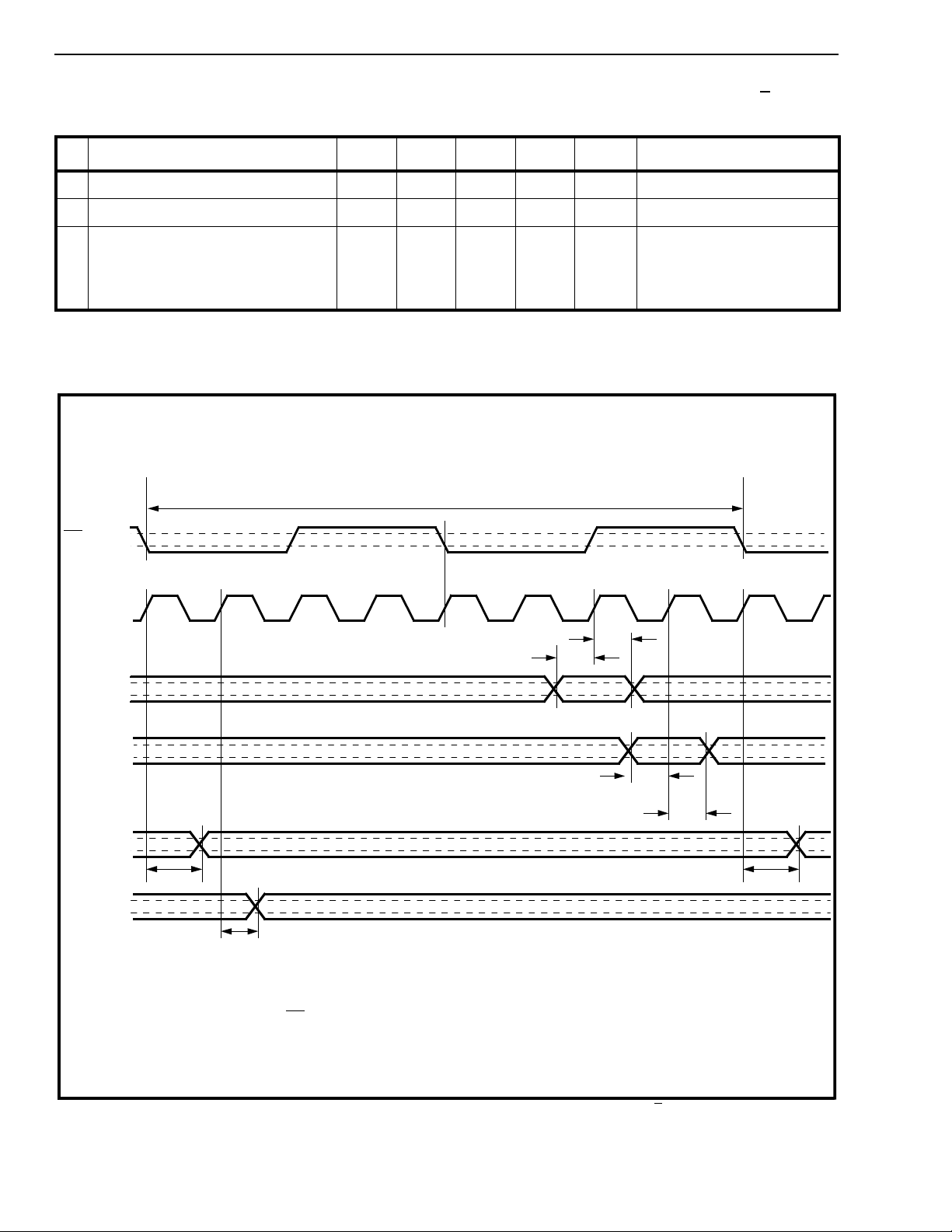
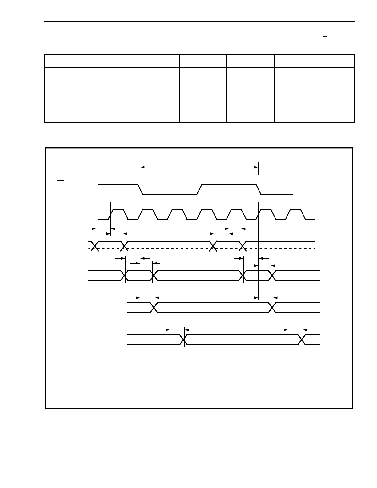
Mbit/s (2/4S= 1). Refer to Figures 3, 4 and 5 for functiona l timing inform ati on.
10 V
SS
Ground.
11-16 S8-S13 Serial Input/Outputs. See des criptio n for pins 2 - 9 above.
17 V
18 V
Supp ly Inpu t . +5V.
DD
Ground.
SS
19-20 S14-S 15 Serial Input/Outputs. See des criptio n for pins 2 - 9 above.
21-26 S16-S 21 Serial Input/Outputs (TTL compatible with internal pullups). Time division, multiplexed serial
bus streams which are configured as inputs in serial to parallel mode (MCA =0), and outputs in
27 V
parallel to serial mode (MCA =1). Data is clocked at 2.048 Mbit/ s (2
outputs are inactive when the device is configu red for 4.096 Mbit/s operation (2
Ground.
SS
/4S = 0). These input/
/4S=1).
28-33 S22-S 27 Serial Input/Outputs. See des cription for pins 21-26 above.
34 V
35 V
Ground.
SS
Supply In pu t +5V.
DD
36-39 S28-S 31 Serial Input/Outputs. See des cription for pins 21-26 above.
40 CKD Clock Delay (Input). Control input which configures internal device timi ng.
CKD=0 Internal master counter is reset at the system frame boundary established by the
frame pulse (F0i
).
CKD=1 Internal master counter is reset one C16 clock period after system frame boundary.
All data input/output wil l be delayed by one C16 clock period.
Timing for data input/output and for OE
phase between the frame boundary establi she d by F0i
DFPo, DFPo
and CFPo is also affected by the state of the CKD input. See descripti ons
is affected by the level asserted on CKD. The relative
and output signals F0o, C2o, C4o,
pertaining to each specific pin for mo re inform at ion.
41 C4i
42 OE
4.096MHz Clock Input. The 4.096 MHz clock signal must be phase locked to the 16.384 MHz.
clock. The falling edge of C4i is used to clock in the frame pulse (F0i
).
Output Enabl e (Input). When low, output data bus (serial or parallel) is actively driven.
When set high, the output bus drivers are disabled. In serial to parallel mode, the outputs are
disabled immediately after OE
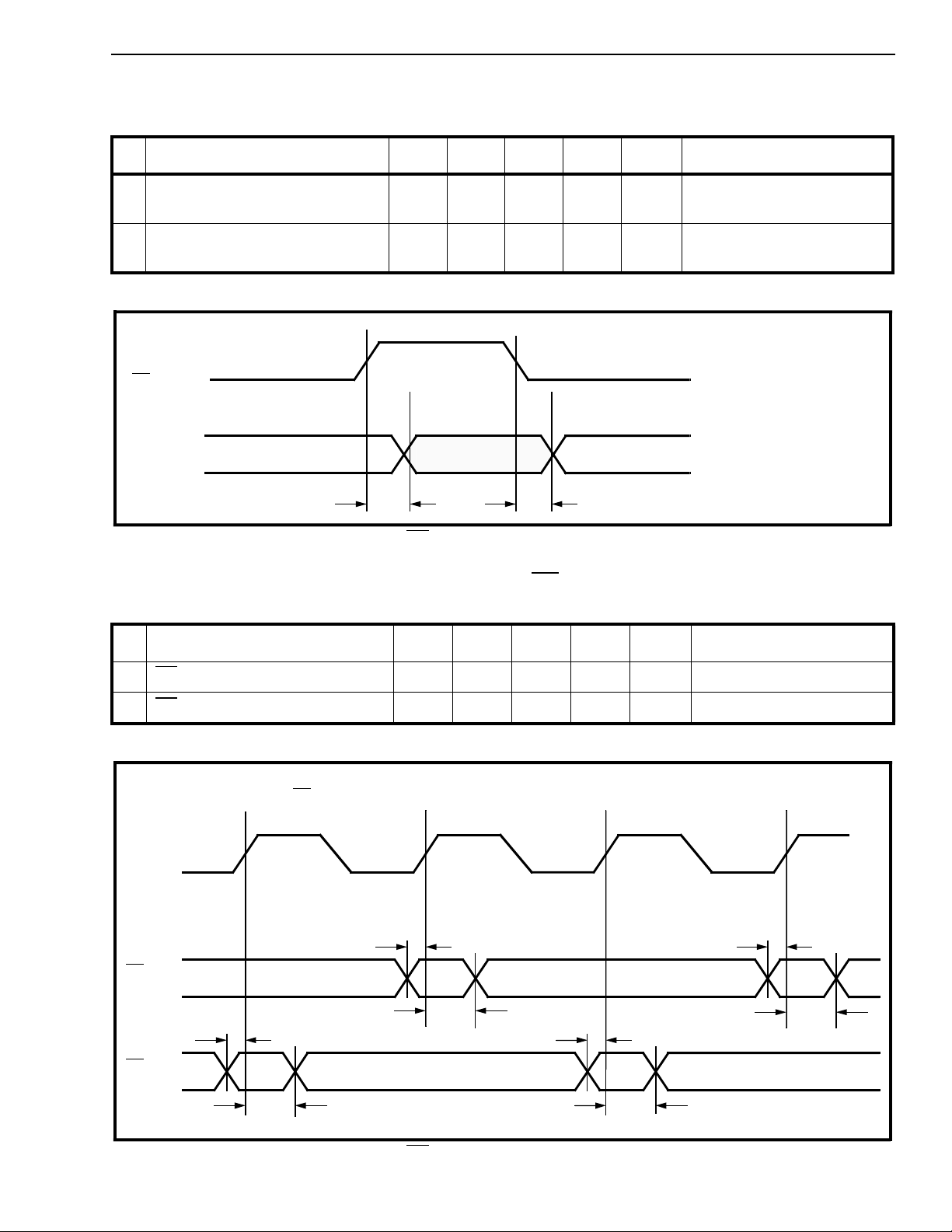
is taken High. See Figures 6 and 21 for timing information
pertaining to parallel t o serial mode .
43 2/4S 2.048/4.096 Mbit/s S ele ct (Inpu t). Selects the data ra te for the time divisio n, multipl exed
serial streams. When tied low, the data rate is 2.048 Mbit/s. When tied high, the dat a rate is
4.096 Mbit/s.
44 MCA Mode Con trol -A (Inp ut). The device will perform a serial to parallel conversion when this
input is tied low. When the input is tied high, the device operates in the parallel to serial m ode.
45 IC Internal Connection. Must be tied to V
for normal device operation.
SS
46 IC Internal Connectio n. Should be left unconnected.
47 CFPo Connect Memo ry Fr am e Pulse (Outpu t). Framing signal wit h a nominal 8 kHz frequency;
goes low 71 (CKD=0) or 68 (CKD=1) C16 clock cycles before the frame boundary establishe d
by F0 i
. The signal is used by the connection memory in a typical 1k or 2k switch configuration.
See Figure 15 for timing inform ati o n.
2-127
Page 4

MT9085 CMOS
Pin Description (continued)
Pin # Name Description
48 DFPo Data Memory Frame Pulse (Output). Framing signal with nominal 4 kHz frequency; changes
state 64 (CKD=0) or 65 (CKD=1) C16 clock cycles after the frame boundary established by F0i
This signal is a complement of DFPo
by SMXs (MT9080s) making up the Data Memory in a typical 1k or 2k switch configuration.
49 F0o Framing Type 0 Signal (Output). 8 kHz framing signal output by the PAC to indicate the
frame boundary synchronized to C16. This framing signal is aligned with C4o
the PAC for use by other devices in a typical switch configuration. Refer to Figures 4 and 5 for
functional timing information.
. See Figure 15 for timing information. The signal is used
and is output by
.
50 F0i
51 C16i 16 MHz Clock Input. The 16.384 MHz clock signal input at this pin must be phase-locked to
52 V
53 V
54 DFPo
55 C4o
56 C2o 2.048 MHz Clock Output. This is a 2.048 MHz clock signal derived from the 16 MHz master
57 NC No Connection .
58 V
59 MCB Mode Control-B (Input). This control input performs two different functions, depending on the
Framing Type 0 Signal (TTL compatib le inpu t ). This input signal establishes the frame
boundary for the serial input/ou tput streams. The first falling edge of C4i
edge of F0i
the 4.096 MHz clock input at C4i
Ground.
SS
Supp ly Inpu t. +5V.
DD
Data Memory Frame Pulse (Output). 4 kHz frami ng signal; changes state 64 (CKD=0) or 65
(CKD=1) C16 clock cycles after the frame boundary established by F0i
compleme nt of DFPo . See Figure 15. The signal is used by SMXs (MT9080s) making up the
Data Mem or y in a typical 2k switch configurat ion.
4.096 MHz Clock Output. This is a 4.096 MHz clock signal derived from t he 16 MHz master
clock input at C16. The falling edge of C4o
pulse output at F0o
clock input. The rising edge of this clock signal occurs in the middle of the regenerated frame
pulse output at F0o
Ground.
SS
state of MCA pin.
In parallel to serial mode (MCA=1), MCB def ines which cloc k edge latches in the data.
MCB=0 Data on the parallel bus is latched into the device with the every second falling
MCB=1 Data on the parallel bus is latched into the device wit h every alternate posit ive
In serial to parallel mode (MCA=0), the MCB pin cont rols the state of the parallel bus d river as
follows:
MCB=0 The output drivers are enabled for only half the timeslo t. The data is clocked
MCB=1 The parallel data bus output drivers are enabled for the duration of the channel
establishes the frame boundaries. Refer to Figure 13 for timi ng informat ion .
. See Figure 13 for timing informat ion .
occurs in the middle of the regenerated frame
. Refer to Figures 4 and 5 for functional timing informati on.
. Refer to Figures 4 and 5 for functional timing informat ion.
edge of C16. See Figure 6.
clock edge.
out on the first falling edge within the tim eslot and disabled on the next falling
edge. See Figure 7.
timeslot (two C16 Clock Periods). The data is clocked out on the first positive
edge within a timeslot and disabled on the last edge.
following the falling
. This signal is a
60-67 P0-P7 Parallel Input/Output Data Bus. This 8 bit data bus is an output in serial to parallel mo de
(MCA=0), and an input in parallel to serial mode (MCA= 1). Dat a is clocked in and out of the
port by the C16 clock. The state of the CKD pin det erm ines the relat ive phase of the critical
clock edges with respect to the frame pulse. All inputs/outputs have internal pullups. Refer to
Figures 6 and 7 for functional timing inform ati on.
68 V
2-128
DD
Supply. +5V.
Page 5

C4
F0
CMOS MT9085
512 C4 Cycles
S0-S31
2
/4S = 0
S0-S15
/4S = 1
2
C16i
C4o
C2o
F0o
Serial I/O
2 Mbit/s
01 310
01 2 3 630
Figure 3 - Serial Input/Output Functional Timing
Frame Boundary Established by F0i
Ch. 31 Bit 1
Ch. 31 Bit 0
Ch. 0 Bit 7
Ch. 0 Bit 6
Serial I/O
4 Mbit/S
C16i
C4o
C2o
F0o
Serial I/O
2 Mbit/s
Serial I/O
4 Mbit/S
Ch. 63 Bit 2 Ch. 63 Bit 1 Ch. 63 Bit 0 Ch. 0 Bit 7 Ch. 0 Bit 6 Ch. 0 Bit 5
Figure 4 - Chann el and Frame Alignment (CKD = 0)
Frame Boundary Established by F0i
Ch. 31 Bit 1
Ch. 63 Bit 2 Ch. 63 Bit 1 Ch. 63 Bit 0 Ch. 0 Bit 7 Ch. 0 Bit 6 Ch. 0 Bit 5
Ch. 31 Bit 0
Ch. 0 Bit 7
Ch. 0 Bit 6
Figure 5 - Chann el and Frame Alignment (CKD = 1)
2-129
Page 6

MT9085 CMOS
A
A
A
AAAA
AAAA
AAAA
AAAA
AAAA
AAAA
AAAA
AAAA
AAAA
AAAA
AAAA
AA
AA
AA
AA
AA
AAAA
A
A
A
A
AAAA
AAAA
A
A
A
A
AAA
AAAA
A
A
A
A
AAA
A
A
A
A
AAA
AAAA
A
A
A
A
AAA
A
A
A
A
AAAA
A
A
A
A
A
A
A
A
A
A
A
A
A
A
A
A
A
A
A
A
AAAA
AAAA
AAAA
AAAA
AAAA
AAAA
AAAA
AAAA
AAA
AAA
AAA
AAA
A
A
A
A
A
A
A
A
AA
AAAA
A
A
A
A
AAAA
AAAA
A
A
A
A
AAA
AAAA
A
A
A
A
AAA
AAAA
A
A
A
A
AAAA
AAAA
A
A
A
A
AAA
AAAA
A
A
A
A
AAA
A
A
A
A
AAAA
AAAA
A
A
A
A
AAA
AAAA
A
A
A
A
AAA
AAAA
A
A
A
A
AAA
AAAA
A
A
A
A
AAA
A
A
A
A
Frame Boundary established by F0i
C16i
CKD=0
Serial
Output
S0-S31
Ch. 31, Bit 0 Ch. 1, Bit 7
64 Cycles
Ch. 0, Bit 7
Parallel
Input
MCB=0
OE
Parallel
Input
MCB=1
OE
CKD=1
Serial
Output
S0-S31
Parallel
Input
MCB=0
OE
Parallel
Input
MCB=1
A
A
A
A
C0S
AAA
AAA
AAA
AAA
AAA
AAA
AAA
AAA
AAA
AAA
AAA
AAA
31
AAA
C1S
A
A
C0S
A
31
A
Ch. 31, Bit 0
AAAA
A
AAAA
A
AAAA
A
C0S
AAAA
A
AAAA
A
AAAA
AAAA
AAAA
AAAA
1
AAA
AAA
AAA
AAA
AA
AA
AA
AA
AAAA
AAAA
AAAA
AAAA
31
C1S
C0S
C1S
AAA
AAA
AAA
AAA
1
31
AAA
AAA
AAA
AAA
0
C1S
C1S
C1S
AAAA
AAAA
AAAA
AAAA
AAA
AAA
AAA
AAA
AAAA
AAAA
AAAA
AAAA
2
0
1
C1S
AA
AA
AA
AA
AAA
AAA
AAA
AAA
AA
AA
AA
AA
AAAA
AAAA
AAAA
AAAA
0
C1S
C1S
AAA
AAA
AAA
AAA
AAA
C1S
AA
AA
AA
AA
AAAA
AAAA
AAAA
AAAA
AAAA
2
0
AAA
AAA
AAA
AAA
AAAA
AAAA
AAAA
1
AAAA
C1S
C1S
C1S
AA
AA
AA
AA
AA
AAAA
AAAA
AAAA
AAAA
AAAA
AAAA
AAAA
AAAA
3
AAA
AAA
AAA
1
AAA
2
Ch. 0, Bit 7
C1S
1
C1S
AAA
AAA
C
AAA
AAA
AA
AA
AA
AA
AAAA
AAAA
AAAA
AAAA
AAA
AAA
AAA
AAA
AAA
1S1
C1S
AA
AA
AA
AA
AAAA
AAAA
AAAA
AAAA
AAAA
3
AAA
AAA
AAA
AAA
2
C1S
C1S
C1S
AA
AA
AA
AA
AA
AAAA
AAAA
AAAA
AAAA
AAA
AAA
AAA
AAA
AAAA
AAAA
AAAA
AAAA
4
2
3
C1S
AA
AA
AA
AA
AAA
AAA
AAA
AAA
AA
AA
AA
AA
AAAA
AAAA
AAAA
AAAA
AAAA
AAAA
AAAA
2
AAAA
AAAA
C1S
C1S
C
4
2
AAA
AAA
AAA
AAA
AAAA
AAAA
AAAA
AAAA
AAAA
1S3
AAA
AAA
AAA
AAA
C1S
C1S
AA
AA
AA
AA
AA
AAAA
AAAA
AAAA
AAAA
3
4
C1S
AA
AA
AA
AA
3
C1S
AAA
AAA
AAA
AAA
AAA
AAA
AAAA
C2S
0
C2S
C2S
C2S
AAA
AAA
AAA
0
AAAA
AAAA
AAAA
1
1
AAA
AAA
AAA
AAA
AA
AA
AA
AA
AAAA
AAAA
AAAA
AAAA
C2S
AA
AA
AA
AA
AAA
AAA
AAA
1
AAA
C
2
Ch. 1, Bit 7
AAA
AAAA
AA
AA
AA
AA
AA
AAA
AAA
AAA
AAA
AAA
AAA
AAA
AAA
C2S
0
C2S
AAA
AA
AAA
AA
AAA
AA
3
AAA
AA
AAA
AAA
AAA
AAA
C2S
AAA
AAA
AAA
AAA
0
AAAA
AAAA
AAAA
AAAA
1
AAA
AAA
AAA
AAA
AAA
AAA
AAA
AAA
AAA
AAA
AAA
AAA
AAA
OE
Notes:
C
- on the parallel inputs indica tes d ata closed in with the edge shown will be clocked out on Seria l Stre am Y, Chann e l X.
XSY
Arrows in the row marked OE
indicate the clock edge which la tche s in the state of the OE pin. CXSY written below the arrow indicates the
serial output channel affected by the OE
serial output drivers for stream 1 during channel 1.
Figure 6 - Functional Data I/O Timing in Parallel to Serial Mode (MCA = 1)
2-130
C1S
1
C1S
2
C1S
3
C1S
4
C2S
1
signal. For example, the level on OE clocked in with edge marked C1S1 will enable or disable the
Page 7
AAAA
AAAA
A
A
A
A
A
A
AAA
AAA
AAA
AAA
AAA
AAA
AAA
AAAA
AAAA
A
A
A
A
A
A
AAA
AAA
AAA
AAA
AAA
AAA
AAA
AAAA
AAAA
AAAA
AAAA
AAAA
AAAA
AAAA
AAAA
AAAA
AAAA
AAAA
AAAA
A
A
A
A
A
A
AAA
AAA
AAA
AAA
AAA
AAA
AAA
AAAA
AAAA
A
A
A
A
A
A
AAA
AAA
AAA
AAA
AAA
AAA
AAA
A
A
A
A
A
AAAA
AAA
AAA
AAA
AAA
AAA
AAA
AAA
AAAA
A
A
A
A
A
AA
AAAA
A
A
A
A
A
AA
AAAA
A
A
A
A
A
AA
AAAA
A
A
A
A
A
AA
Frame Boundary established by F0i
C16
CMOS MT9085
Serial
Input
S0-S31
Parallel
Output
MCB=0
CKD=0
Parallel
Output
MCB=0
CKD=1
Parallel
Output
MCB=1
CKD=0
Parallel
Output
MCB=1
CKD=1
Ch.31
AAA
AAA
AAA
AAA
AAA
C30S
Bit 0
31
AAAA
AAAA
AAAA
AAAA
AAAA
AAAA
C30S
C30S
AAA
AAA
AAA
AAA
AAA
AAA
Ch. 0, Bit 7
AAAA
AAAA
AAAA
AAAA
AAAA
AAAA
C
31S0
AAA
AAAA
A
AAA
AAAA
A
AAA
AAAA
AAA
AAA
C31S
AAAA
AAAA
A
A
A
0
31
31
AAAA
AAAA
AAAA
C31S
C31S
AAAA
AAAA
AAAA
AAAA
0
C31S
1
AAA
AAAA
A
AAA
AAAA
A
AAA
AAAA
AAA
AAA
C31S
AAAA
AAAA
A
A
A
1
0
AAAA
AAAA
AAAA
AAAA
AAAA
C31S
AAAA
AAAA
AAAA
AAAA
AAAA
AAAA
C31S
1
1
Note: CxSY - indicates data being output is sourced from Serial Stream Y, Channel X
C31S
AAA
AAA
AAA
AAA
AAA
C31S
AAAA
AAAA
AAAA
AAAA
AAAA
Ch.0
Bit 6
AAAA
AAAA
AAAA
AAAA
AAAA
2
A
A
C31S
A
A
A
2
C31S
C31S
3
AAA
AAAA
A
AAA
AAAA
A
AAA
AAAA
AAA
AAA
C31S
AAAA
AAAA
A
A
A
3
2
2
AAAA
AAAA
AAAA
C31S
C31S
AAAA
AAAA
AAAA
AAAA
3
3
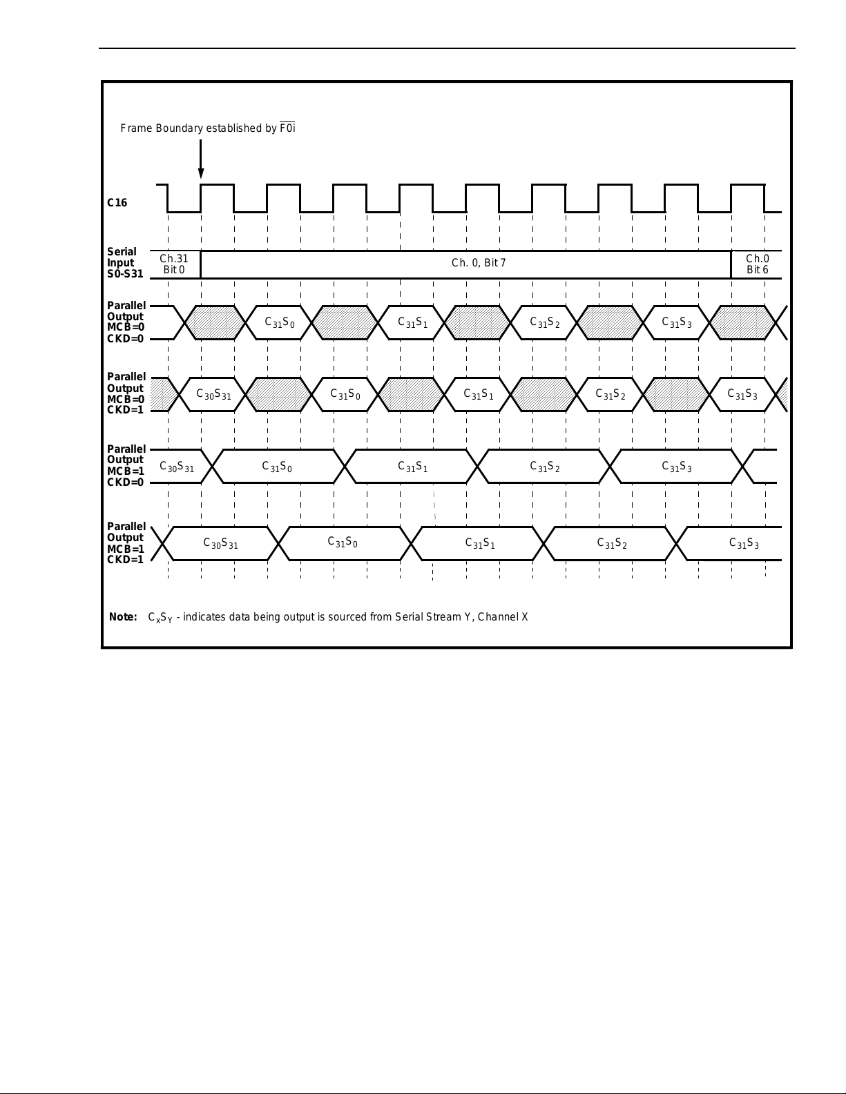
Figure 7 - Functional Data I/O Timing in Serial to Parallel Mode (MCA = 0)
2-131
Page 8
MT9085 CMOS
Functional Description
The MT9085 Parallel Access Circuit (PAC) is a 68
pin monolithic device. It interfaces a parallel 8 bit,
time division, multiplexed bus to 32 or 16 time
division multiplexed serial streams. The device can
be configured to perform either parallel to serial
conversion or serial to parallel conversion. A single
PAC device can handle 1024 channels. The data on
the parallel bus is in a forma t suitable for interfacing
with the Mitel MT9080 Switch Matrix M odule (SMX).
The data rate on the serial streams can be selected
to be 2.048 or 4.096 Mbit/s.
The serial input/output format conforms to the
ST-BUS requirements when the data rate is 2.048
Mbit/s (see Figure 3). The ST-BUS is a
time-division, multiplexed serial bus with 32, eight bit
channels per frame. Frame boundaries are
delinated by the frame pulse. Data on the serial
streams is clocked in and out with the C16i clock.
When the device is configured for 4.096 Mbit/ s data
rate operation, the first 16 (S0-S15) of the 32 serial
streams are used. Each of the 16 time-division
multiplexed serial streams is made up of 64
channels. Data is clocked in or out with the C16i
clock.
Parallel To Serial Conversion
The MT9085 can be configured to perform parallel to
serial conversion by tying the MCA input high.
Contiguous channels clocked into the device are
output on the serial streams in an interleaved
manner on each of the serial outputs. For example
when the device is configured for 2.048 Mbit/s data
rate, the first 32 parallel channels clocked into the
device will be clocked out during channel 0 on serial
streams 0 to 31. Channel 1 on serial streams 0 to 31
will contain data from the next 32 timeslots. On any
single serial stream, consecutive output channels
are sourced from every 32nd parallel input channel
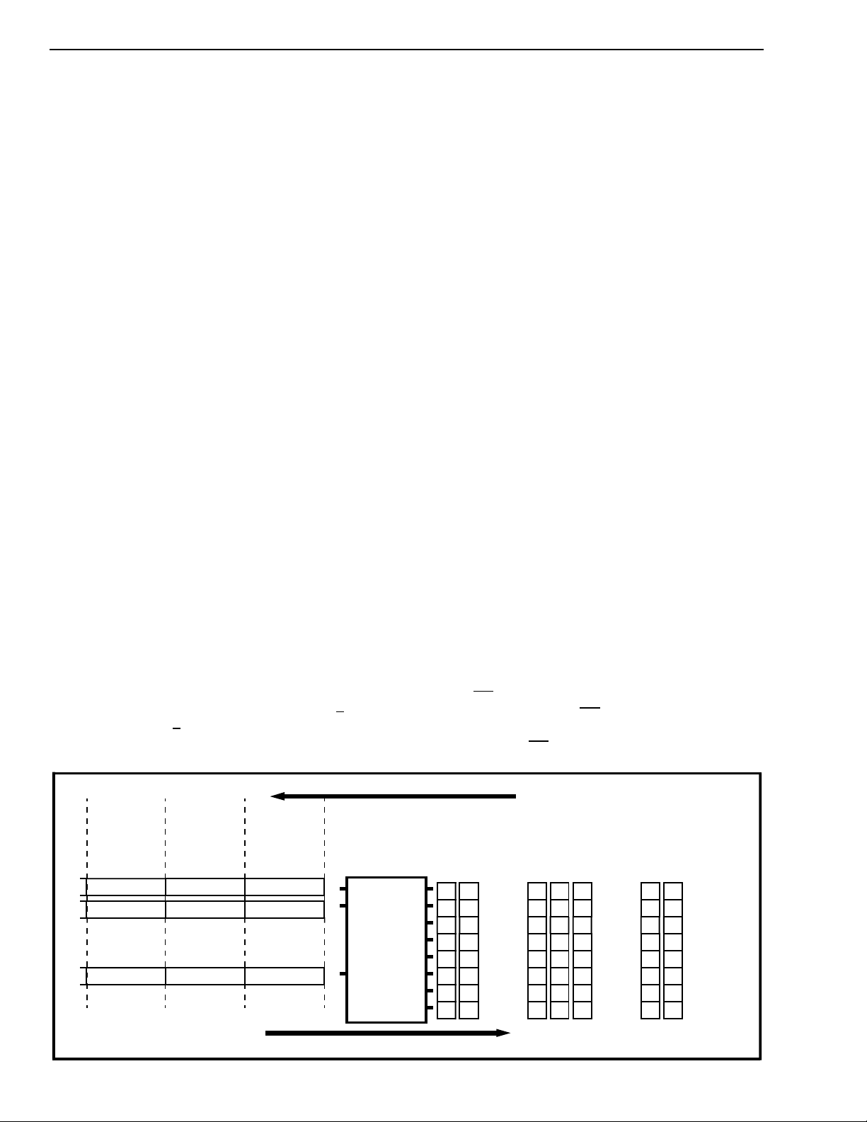
(see Figures 6 and 8). When the device is
configured for 4.096 Mbit/s serial output operation,
contiguous channels on the serial streams are
sourced from every 16th parallel input channel.
Data on the eight bit parallel bus is clocked into the
device with the C16 clock. The level asserted on the
MCB input specifies whether the data is clocked into
the device on the falling edge or the rising edge of
C16. The relative phase of the critical edge with
respect to the system frame boundary is defined by
the level asserted on the CKD pin as illustrated in
Figure 16. The flexibility in input timing permits the
PAC to be easily interfaced to the SMX in 1024 and
2048 switching applications. Refer to the
applications section of this data sheet for more
details.
The delay through the PAC is approximately one
ST-B US channel time when the device is operat ed in
2.048 Mbit/s mode, i.e., any specific channel clocked
into the device will be clocked out one ST-BUS
channel later. In the 4.096 Mbit/s mode, the delay is
equal to eight C4 clock cycles.
Data on the eight bit parallel bus (P0-P7) is clocked
into the device with the C16i clock. It is clocked out
on the serial s treams at either 2.048 Mbit/s (2
or at 4.096 Mbit/s (2
/4S=1). See Figures 16, 17 and
/4S =0)
19 for t im i ng i n fo rmation.
Parallel to Serial Conversion
CH. 2
0 1 2 3 4 5 6 7
TS64
TS65
•
•
•
•
•
•
•
•
TS95
CH. 1
0 1 2 3 4 5 6 7
TS32
TS33
•
•
•
•
TS63
CH. 0
0 1 2 3 4 5 6 7 Bit #
TS0
TS1
•
•
•
•
TS31
Serial to Parallel Conversion
S0
S1
•
•
•
•
S31
PAC
Figure 8 - PAC Operatio n at 2.04 8 Mb it/s
Serial output channel timeslots can be tri-stated by
setting OE
timeslot . T h e tim in g fo r O E
high during a specific parallel channel
is described in Figures 6
and 21. Note that the level asserted on MCB affect s
the operation of OE
TS0TS
P0
P1
P2
P3
P4
P5
P6
P7
1
0
0
1
1
2
2
3
3
4
5
6
7
•••
4
5
6
7
.
TS31TS32TS
0
0
1
1
2
2
3
3
•
4
4
5
5
6
6
7
7
33
TS63TS
64
0
0
1
2
3
•••
4
5
6
7
0
1
1
2
2
3
3
•
4
5
6
7
•••
4
5
6
7
•
2-132
Page 9

Serial to Parallel Conversion
The MT9085 can be configured to perform serial to
parallel conversion by tying the MCA pin low. A
single PAC will accept 1024 channels on the 32 or 16
serial streams and output the data onto the parallel
bus as illustrated in Figure 8.
CMOS MT9085
The PAC outputs ST-BUS timing signals, F0o
and C4o
between the frame boundary established by F0i
F0o
Applications
derived from C16i. The phase relationship
is illustrated in Figures 4 and 5.
, C2o
and
The data on the serial input streams can be clocked
in at 2.048 Mbit/s or at 4.096 Mbit/s by setting the
appropriate level on the 2
and 17 for timing details.
Data is clocked out on the parallel bus with the C16
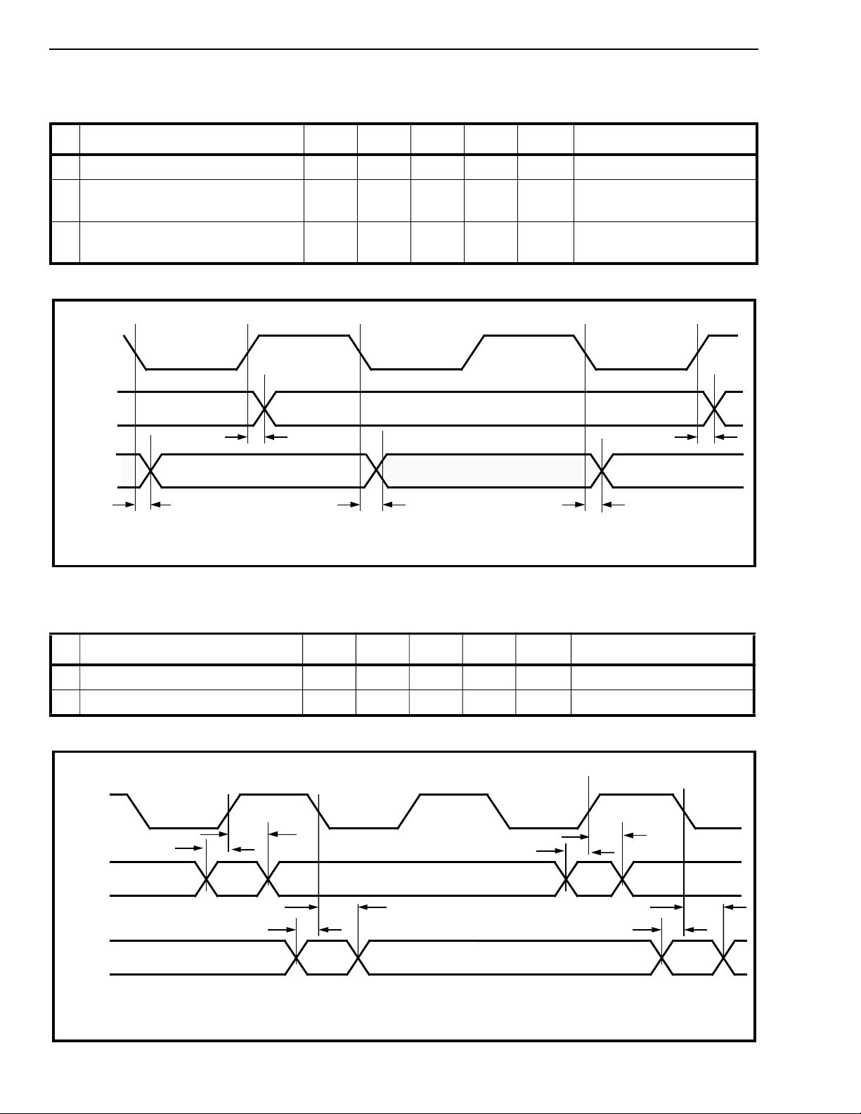
clock (see Figure 18 for timing details). The parallel
output bus will be actively driven for two C16 clock
periods when MCB is tied high. Data is output with
every second rising clock edge. Setting MCB low
will enable the output drivers for only one C16 clock
period in any specific parallel channel timeslot. The
actual phase relationship between the system frame
boundary and the parallel out put timeslots is affected
by the level asserted on the CKD input (see Figure
7). The flexibility in output timing permits the PAC to
be easily interfaced to the SMX in 1024 and 2048
channel configurations. Refer to the applications
section of this data sheet for more information.
The delay through the PAC is approximately one
ST-BUS channel when the device is configured for
2.048 Mbit/s serial rate. In the 4.096 Mbit/s mode,
the delay is equal to approximately eight C4 clock
cycles.
Timing and Framing Signa ls
The PAC requires two clock signals. A 16.384 MHz
master clock (C16) is used to clock data in and out of
the device on the parallel bus. A 4.096 MHz clock
(C4i
), phase locked to C16i, clocks in the frame
pulse. The positive C16i edge immediately after the
C4i
falling edge which clocks in F0i defines the
internal frame boundary. The two separate clock
inputs permit synchronization of the MT9085 to
system timing in which the frame pulse is derived
from a 4.096 MHz clock.
The PAC generates all framing signals necessary to
construct a 1024 channel or a 2048 channel switch
matrix using the S MX. The DFPo signal is used as
a framing signal for the SMXs operated as the Data
Memory. The CFPo is used to synchr onize Co nnect
Memory timing in a typical 1K or 2K switch
application (refer to the application section in this
data shee t for more infor mation). Th e timing of bo th
DFPo and CFPo signals is affected by the level
asserted on the CKD input as s hown in Figure 15.
/4S pin. See Figures 16
1024 Chann el Digi tal Time-Sp ace Sw itch
A 1024 channel serial time-space digital switch
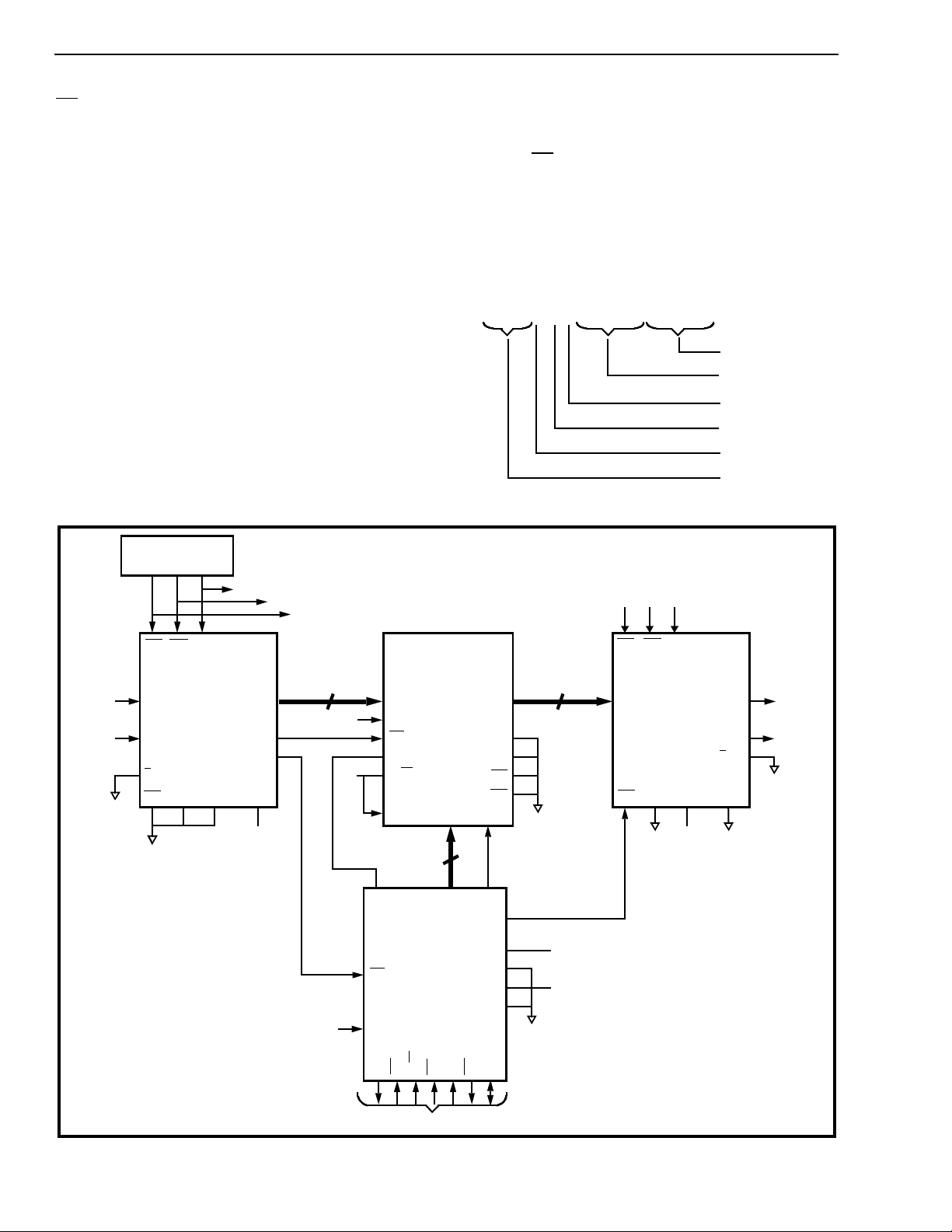
design is illustrated in Figure 9.
The main switching function is accomplished using
two MT9080s (SMXs). One SMX is operated in the
Data Memory mode and the second serves as the
Connection Memory. Refer to the SMX data sheet
for more information on this configuration. The serial
to parallel conversion function is provided by a PAC
configured for 2.048 Mbit/s operatio n (2
MCB input in this PAC is tied high to ensure data
output by the PAC meets SMX input setup and hold
requirement . PAC #2 performs the parallel to serial
function; MCA is set high. The MCB input in this
device is set low to allow dat a to be clocked in with
the falling edge of C16.
The main timing source generates a 16.384MHz
clock phase locked to a 4.096MHz clock. The
framing signal input to PAC#1 at F0i
requirements specified in Figure 13 of this data
sheet. In some applications where a master 16.384
MHz oscil la to r i s u se d f or sys te m timing, th e C4i
F0i
clocks could be derived directly from it. In
applications where a 4.096 MHz clock signal is
available, the 16.384 MHz clock can be generated
using a phase-lock loop.
Framing signals for both the SMXs are generated by
PAC #1. DFPo is connected to FP
Memory. CFPo is con nected to the F P input of the
Connection Memory. PAC #2 is configured to
perform parallel to serial conversion.
The DFPo and CFPo signals ensure that all timing
requirements necessary to interface the SMXs with
the PACs are met while input and output serial
frames are aligned.
The maximum delay through the switch is
approximately one frame plus two serial channels
when SMX#1 is operated in Data Memory Mode-1.
When the SMX is operated in Dat a Memory Mode-2,
the maxim um delay is two frames. In this case, the
channels are double buffered; frame integrity is
maintained for all switching configurations.
/4S = 0). The
should meet the
and
input of the Data
2-133
Page 10
MT9085 CMOS
In the example c onfiguration shown in Figure 9 the
pin of PAC #2 is connected to D10 on the
OE
Connection Memory. Setting bit 10 high in the
Connection Memory location corresponding to a
serial channel timeslot will result in the output driver
for the specific stream being disabled during that
serial cha nne l timeslot. D11 is conn ecte d to the ME
input of SMX1 and D12 is connected to a mode
select pin (Mz). Consequently, the levels on these
outputs can be set high or low by writing to the
appropriate memory location corresponding to the
selected output channel. The mapping of the control
functions on to Connection Memory data bits is
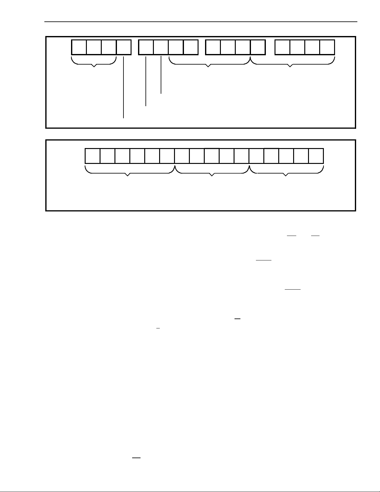
illustrated in Figure 10.
The data on the PAC serial streams is byte
interleaved as described in the Functional
Description section in this data sheet. The SMX
channel number corresponding to the channel on the
serial streams can be determined directly by
specifying the serial channel and stream number in
binary as shown in Figure 11. For example, serial
channel 4, stream 2 corresponds to SMX channel
number Hex 0082. In order to program the matrix for
switching, the input channel address is writ ten to the
Connection Memory address corresonding to the
serial output channel. The bits controlling features
such as OE
, ME, and Mz should be set or reset
accordingly at the same time. For example. if
channel 4 on stream 2 is to be switc hed to channel
10 on stream 1, the following binary word is written
to Connection Memory address corresponding to the
output channel (Hex 0141):
XXX0 10000000 0010
Stream Address
Channel Address
Output Enable
Message Enable
DM-1/DM-2
Unused
S0
S31
Timing
Source
C16
C4
F0
C4i
•
•
•
•
/4S
PAC#1
CKD
C16i
S/P
MCA
P0-P7
DFPo
CFPo
MCB
+5
C16
SMX # 1
DM - 1/2
8
C16
+5
D0-D7i
CK
FP
Mz
R/W
ODE
D12 D0-D9 D11
SMX #2
CM - 1
FP
CONNECTION
MEMORY
CK
DATA
MEMORY
A0-A9
D0-D7o
Mx
My
CS
DS
ME
10
D10
ODE
Mx
My
Mz
8
+5
+5
F0i
S0
•
•
•
•
S31
2
OE
From Timing Source
F0 C4 C16
C4i C16i
F0i
PAC#2
P/S
P0-P7
OE
CKD
MCA
+5
S0
S31
2
/4S
MCB
S0
•
•
•
•
•
•
•
•
S31
2-134
DTADSR/W
CS
A0-A15CDD0-D15
MPU Interface
NOTE: Connect all inputs not shown to V
Figure 9 - 102 4 Chan nel Sw itch Matrix Using th e PAC and SMX
SS
Page 11
CMOS MT9085
15141312 111098 7654 3210
Not
Used
OE - Output Enable
ME - Message Enable
Mode Contro l - DM-1 or DM-2
Serial Channel
Number
Stream
Address
Figure 10 - Mapping of Data Memory and PAC Control Functions on C onnection Memory Data Bits
43 21043210
Unused Channel
Ex. Serial Stream 4, Channel 3 Corresponds to SMX Channel Number 100 (Hex 0064)
Address
Stream
Address
Figure 11 - Decoding SMX Channel Number from Serial Stream & Channel Address
1024 Switch Conf igura tion
2048 Chann el Digi tal Space -Time Sw itch
Application
applications where a master 16.384 MHz oscillator is
used for system timing, the C4i
and F0i clocks could
be derived directly from it.
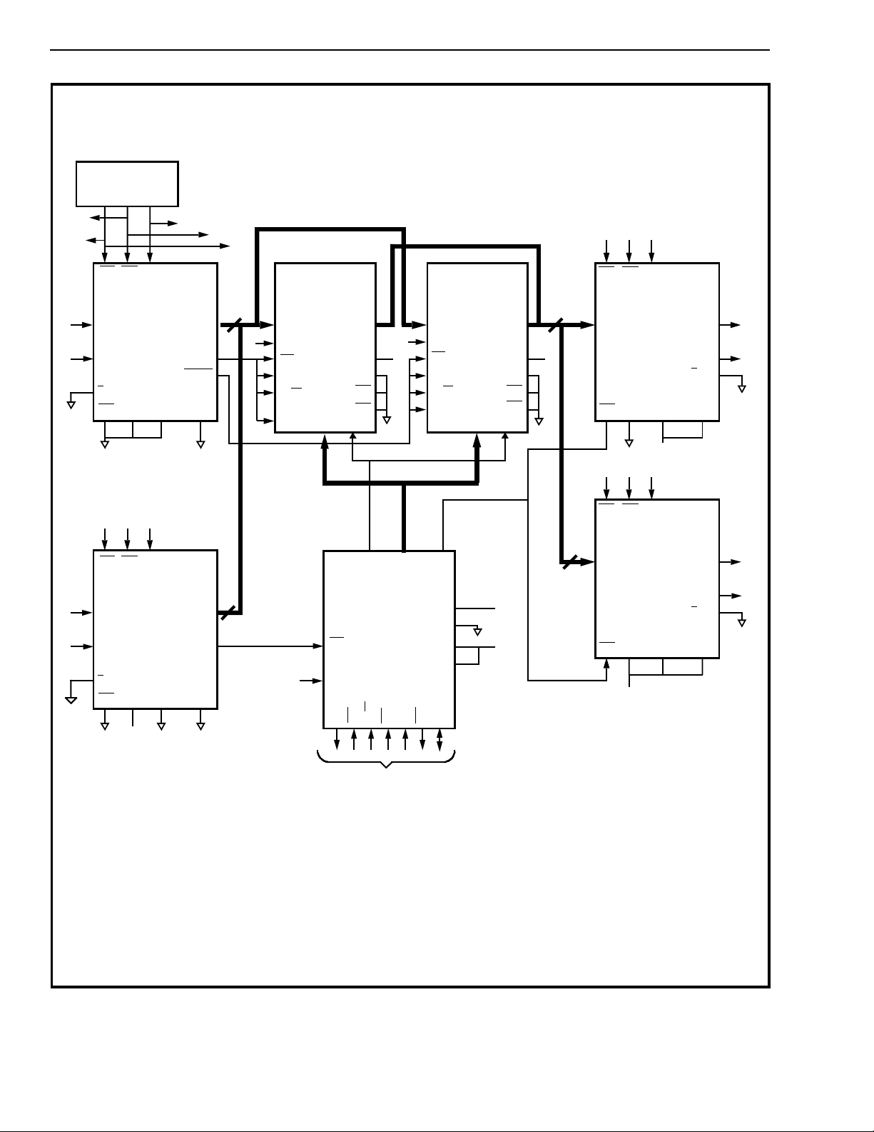
A 2048 channel serial time-space digital switch
design is illustrated in Figure 12.
The DFPo and DFPo generated by PAC #1a are
used to switch the mode of operation of the Data
The main switching function is accomplished using
three MT9080s (SMXs). Two SMXs function as the
data memory, while the third is operated in Connect
Memory mode. Refer to the SMX data sheet for
more information on this configuration. The Serial to
parallel conversion for 2048 channels is handled by
two PACs. PAC #1a and PAC #1b. Both are
configured for 2.048 Mbit/s operation (2
/4S=0). The
MCB input is tied low in both devices. The parallel
data bus on each of the devices will be actively
driven for one C16 clock period. The CKD input is
set low in one of the devices and set high in the
other. This will cause the output timing of the two
PACs to be off set by one C16 clock period.
Memory SMXs between Counter and External
modes and also serve as the frame pulse for the two
SMXs. Because D FPo and DFPo
are complementary
signals, one of the two SMXs is operated in the
Counter mode while the second one is operated in
the External mode. The states of the other c ontrol
inpu t s, R/W
and ODE, are changed accordingly.
The SMX configured as the Connection Memory, is
fed a frame pulse from PAC #1b. The phase
alignment of CFPo with respect to DFPo ensures
that timing requirements for proper operation of the
SMXs are met. Refer to the SMX data sheet for
more information on the timing requirements.
Consequently, the parallel output of one device will
be disabled while the other is active.
The maximum delay through the switch is two
frames. Channels are double buffered and frame
The parallel to serial conversion is also
accomplished with two PACs. Data from the
integrity is maintained for all switching
configurations.
common SMX parallel bus is clocked into each PAC
in alternate clock periods.
The timing source generates a 16.384 MHz clock
phase locked to a 4.096 MHz clock. The framing
signal input to PAC #1a at F0i
should meet the
For more information, see Mitel’s Application Note
MSAN-135,
Matrices using the SMX/PAC“
and Application Sheet MSAS-62
Generation fo r SM X /PAC“
“Design of Large Digital Switching
(in this data book)
“16.384 MHz Clock
(available from Mitel).
requirements specified in this data sheet. In some
2-135
Page 12
MT9085 CMOS
Timing
Source
M4
MF
S0
S31
S0
S31
F0i
S0
•
•
•
•
•
•
•
•
S31
2
/4S
OE
F0 C4 C16
F0i
S0
•
•
•
•
•
•
•
•
S31
2
/4S
OE
C4i
PAC#1a
CKD
C4i
PAC#1b
CKD
+5
C16i
S/P
MCA
C16i
S/P
MCA
C16
P0-P7
DFPo
DFPo
MCB
P0-P7
CFPo
MCB
C4
From Timing Source
8
F0 C4 C16
C4i C16i
F0i
PAC#2a
P/S
P0-P7
OE
CKD
MCA
F0 C4 C16
F0i
C4i C16i
PAC#2b
P/S
P0-P7
OE
CKD MCA
+5
+5
S0
S31
2
/4S
MCB
S0
S31
/4S
2
MCB
S0
•
•
•
•
•
•
•
•
S31
S0
•
•
•
•
•
•
•
•
S31
F0
SMX #1
CNT/EXT
8
8
C16
D0-D7i
CK
FP
Mz
R/W
ODE
C16
A0A10
CK
D0-D7o
ME
FP
DTADSR/W
C16
+5
Mx
My
CS
DS
D12
D0-D10 D11
SMX #3
CM - 2
CONNECTION
MEMORY
CS
A0-A15CDD0-D15
D0-D7i
CK
FP
Mz
R/W
ODE
ODE
Mx
My
Mz
SMX #2
CNT/EXT
D0-D7o
A0A10
ME
+5
+5
Mx
My
CS
DS
8
+5
NOTE: Connect all inpu ts not shown to V
Figure 12 - 2048 C hannel Switch Matrix Using the PAC and SMX
2-136
MPU Interface
SS
Page 13
CMOS MT9085
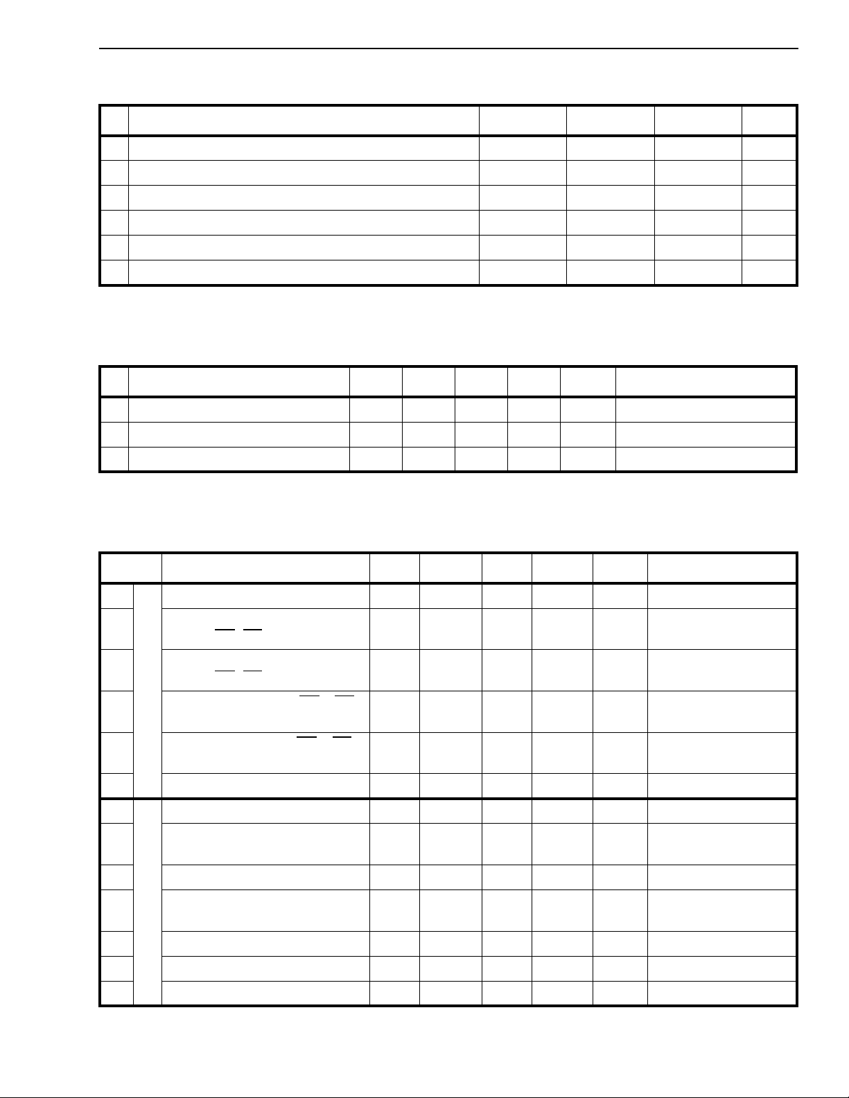
Absolute Maximum Ratings* - Vo ltage s are with respe ct to Ground (V
) unless otherwise stated .
SS
Parameter Symbol Min Max Units
1V
DD-VSS
2 Voltage on Digital Inputs V
3 Voltage on Digital Outputs V
4 Current at Digital Outputs I
5 S torage Temperature T
6 Package Power Dissipation P
* Exceeding these values ma y cause perm anen t dama ge. Functi onal operati on und er these cond ition s is not implied.
I
O
O
S
D
Recommended Operating Conditions - Voltages are with respect to Ground (V
Characteristics Sym Min Typ
1 Operating Tem peratu re T
2 Positive Supply V
OP
DD
3 Input Voltage V
‡ Typical figures are at 25°C and are for design aid only: not guaranteed and not subject to producti on testing.
-40 70 °C
4.5 5.5 V
I
0V
‡
Max Units Test Conditions
DD
-0.3 7 V
VSS-0.3 VDD+0.3 V
VSS-0.3 VDD+0.3 V
-40 125 °C
) unless otherwise stated.
SS
V
40 mA
2W
DC Electrical Characteristics - Voltages are with respect to Ground (V
Characteristics Sym Min Typ
1
2 I nput High Voltage - all pins
Supply Current I
except C4i
, F0i, S0-S31
V
DD
IH
0.7V
DD
) unless otherwise stated.
SS
‡
Max Uni ts Test Condi tions
50 m A Outputs unloaded
V
I
3 Inpu t Low Voltage - all pins
N
except C4i
P
U
4 Input High Voltage - C4i
T
S0-S31
, F0i, S0-S31
, F0i,
V
IL
V
IH
00.3V
DD
V
2.0 V
S
5 Inpu t Low Voltage - C4i
, F0i,
V
IL
0.8 V
S0-S31
6 Inpu t Leakage Current I
7
Output Low Current S0-S31 I
8 O ut put Low Current all output s
except S0-S31
O
U
9 O ut put High Current S0-S31 I
T
10 Output High Current all outputs
P
except S0-S3
U
T
11 High Impeda nce Leakage IOZ 10 µA
S
12 Inpu t Pin Capacitance C
13 Out put P in Capacit an ce C
‡ Typical figures are at 25°C and are for design aid only: not guaranteed and not subject to producti on testing.
I
I
IL
OL
OL
OH
OH
8mAV
8mAV
8mAV
8mAV
i
o
10 pF VDD=5.0V ±10 %
±10 µA
10 pF
OL
OL
OH
OH
=0.4V
=0.3V
=2.4V
=0.7V
DD
DD
2-137
Page 14
MT9085 CMOS
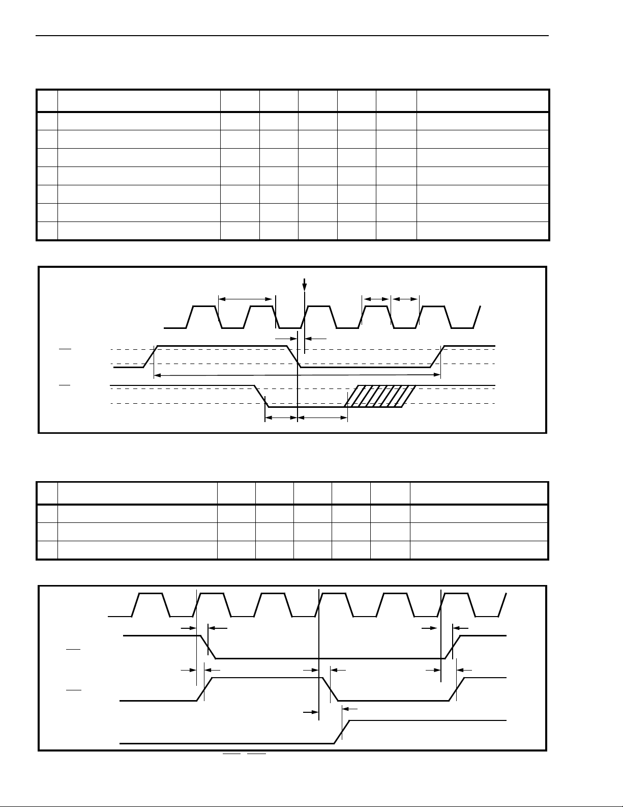
AC Electrical Characteristics†- Input Frame Pulse and Clock Timing (See Figure 13) -
Voltages are with respect to Ground (VSS) unless otherwise stated.
Characteristics Sym Min Typ
‡
Max Units Test Conditions
1 C16 Clock Period t
2 C4 Clock Period t
3 C16 Pulse Width Low t
4 C16 Pulse Width High t
5 C4 Setup Time t
6 Frame Pulse Setup Time t
7 Frame Pulse Hold Time t
† Timing is over recommended temperature & power supply voltages.
‡ Typical figures are at 25°C and are for design aid only: not guaranteed and not subject to producti on testing.
C16i
C4i
F0i
C16P
C4P
C16L
C16H
C4S
FPS
FPH
t
C16P
60 61 62 ns
219 244 269 ns
25 ns
25 ns
-10 25 ns
5200ns
5ns
ST-BUS Frame Boundary
t
C16HtC16L
t
C4S
t
C4P
t
FPS
t
FPH
Figure 13 - ST-BUS Frame Pulse and Clock Timing
AC Electrical Characteristics† - Output Clocks and Frame Pulse Timing (See Figure 14) -
Voltages are with respect to Ground (V
Characteristics Sym Min Typ
1 Frame Pulse Delay t
2 C4 Clock Delay t
3 C2 Clock Delay t
† Timing is over recommended temperature & power supply voltages.
‡ Typical figures are at 25°C and are for design aid only: not guaranteed and not subject to producti on testing.
C16i
F0o
C4o
) unless otherwise stated.
SS
t
FPD
t
C4D
FPD
C4D
C2D
‡
Max Units Test Con ditio ns
031nsC
028nsC
0nsC
t
C4D
t
C2D
=85pF
L
=85pF
L
=85pF
L
t
FPD
t
C4D
2-138
C2o
Figure 14 - F0o, C4o and C2o Output Clock Timing
Page 15
CMOS MT9085
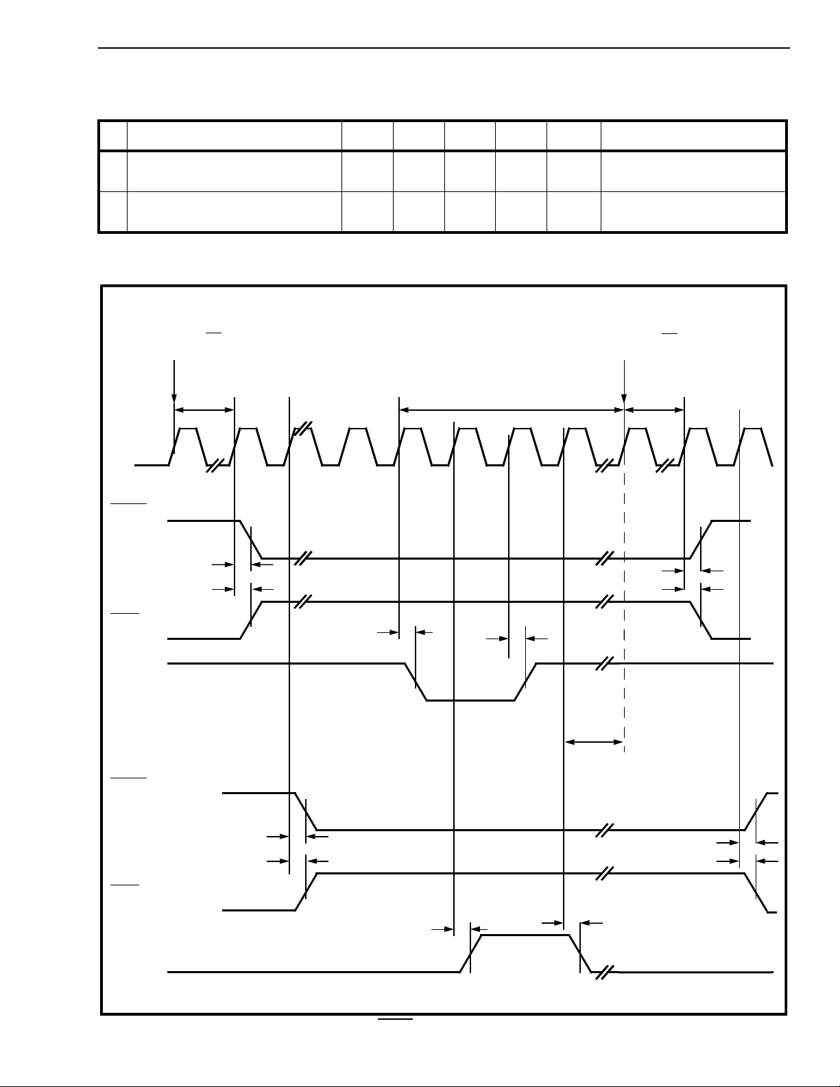
AC Electrical Characteristics† - Data Memory and Connect Memory Frame Pulse (See
Figure 15) - Voltages are with respect to Ground (V
Characteristics Sym Min Typ
) unless otherwise stated.
SS
‡
Max Units Test Conditions
1 Data - Memory Frame Pulse
t
DFPo
037nsC
=85 pF
L
Delay
2 Connection - Memory Frame
t
CFPo
030nsC
=85 pF
L
Pulse Delay
† Timing is over recommended temperature & power supply voltages.
‡ Typical figures are at 25°C and are for design aid only: not guaranteed and not subject to producti on testing.
ST-BUS Frame Boundary
Established by F0 i
64 C16
Cycles
C16i
CKD=0
DFPo
t
DFPo
t
DFPo
71 C16 Cycles
ST-BUS Frame Boundary
Established by F0i
64 C16
Cycles
t
DFPo
t
DFPo
DFPo
CFPo
CKD=1
DFPo
DFPo
CFPo
t
DFPo
t
DFPo
t
CFPD
t
CFPo
t
CFPD
68 C16
Cycles
t
CFPo
t
DFPo
t
DFPo
Figure 15 - DFPo and CFPo Output Timing
2-139
Page 16
MT9085 CMOS
AC Electrical Characte rist ics† - Serial Input and Out put Timing in 2 MHz Mode (2/4S=0)
(See Figur e 16) - Voltages are with respect to Ground (V
Characteristics Sym Min Typ
) unless otherwise stated.
SS
‡
Max Units Test Conditions
1 Serial Input Setup Time t
2 Serial Input Hold Time t
3 Serial Output Dela y
SS
SH
t
SD
Active to Active
High Impedance to Active
Active to High Impedance
† Timing is over recommended temperature & power supply voltages
‡ Typical figures are at 25°C and are for design aid only: not guaranteed and not subject to producti on testing.
C4i
C16i
S0i-S7i
(CKD=0)
0ns
24 ns
Serial Bit Cell
47
47
44
t
t
SS
SH
ns
ns
ns
CL=150pF
C
C
=150pF
L
=150pF
L
S0i-S7i
(CKD=1)
t
SS
t
SH
S0o-S7o
(CKD=0)
t
SD
S0o-S7o
(CKD=1)
t
SD
Note: 1) The phase relationship of C4i and C16i depends on the user’s timing source (see Fig. 13 for device related contstraints).
2) Timing measurements for inputs are referenced to/from a low voltage of 0.8V and a high voltage of 2.0V.
Measurements for outputs are referenced to/from a low voltage of 0.4V to a high voltage of 2.4V
Figure 16 - Serial Input and Output Timing in 2 Mbit/s Mode (2/4S=0)
t
SD
2-140
Page 17
CMOS MT9085
AC Electrical Charact eristics† - Serial Inp ut and Output Timing in 4 MHz Mode (2/4S=1)
(See Figur e 17) - Voltages are with respect to Ground (V
Characteristics Sym Min Typ
) unless otherwise stated.
SS
‡
Max Units Test Conditions
1 Serial Input Setup Time t
2 Serial Input Hold Time t
3 Serial Output Delay
t
SS
SH
SD
Active to Active
High Impedance to Active
Active to High Impedance
† Timing is over recommended temperature & power supply voltages
‡ Typical figures are at 25°C and are for design aid only: not guaranteed and not subject to producti on testing.
C4i
C16i
t
S0i-S7i
(CKD=0)
S0i-S7i
(CKD=1)
SS
t
SS
t
SH
t
SH
0ns
24 ns
Serial Bit Cell
t
SS
47
47
44
t
SS
ns
ns
ns
t
SH
CL=150pF
C
C
t
SH
=150pF
L
=150pF
L
t
SD
S0o-S7o
(CKD=0)
t
SD
S0o-S7o
(CKD=1)
Note: 1) The phase relationship of C4i and C16i depends on the user’s tim ing source (see Fig. 13 for device related contstraints).
2) Timing measurements for inputs are referenced to/from a low voltage of 0.8V and a high voltage of 2.0V.
Measurements for outputs are referenced to/from a low voltage of 0.4V to a high voltage of 2.4V
t
SD
t
SD
Figure 17 - Serial Input and Output Timing in 4 Mbit/s Mode (2/4S=1)
2-141
Page 18
MT9085 CMOS
AC Electrical Characte ristics† - Parallel Output Timing (See Figure 18) - V oltages are with respect
to Ground (V
) unless otherwise stated.
SS
Characteristics Sym Min Typ
‡
Max Units Test Conditions
1 Parallel Output Delay t
2 Parallel Output Delay
t
PZA
PD
28 ns CL=85pF
28 ns CL=85pF
High Impedance to Active
3 Parallel Output Delay
t
PAZ
28 ns CL=85pF
Active to High Impedance
† Timing is over recommended temperature & power supply voltages
‡ Typical figures are at 25°C and are for design aid only: not guaranteed and not subject to producti on testing.
C16i
P0 to P7
MCB=1
t
PD
P0 to P7
MCB=0
t
PZA
NOTE: See Figure 7 for functional timing information
t
PAZ
90%
10%
t
PZA
t
PD
Figure 18 - Parallel Output Timing
AC Electrical Characteristi cs† - Parallel Input Timing (See Figure 19) - Voltages are with respect to
Ground (V
1 Parallel Input Setup Time t
2 Parallel Input Hold Time t
† Timing is over recommended temperature & power supply voltages.
‡ Typical figures are at 25°C and are for design aid only: not guaranteed and not subject to producti on testing.
C16i
P0 to P7
MCB=1
P0 to P7
MCB=0
) unless otherwise stated.
SS
Characteristi cs Sym Min Typ
PS
PH
t
PH
t
PS
t
PS
‡
Max Units Test Conditions
0ns
5ns
t
PH
t
PS
t
PH
t
PS
t
PH
NOTE: See Figure 6 for functional timing information
Figure 19 - Parallel Input Tim ing
2-142
Page 19
CMOS MT9085
AC Electrical Characteristics† - Output Enable Timing, Seri al to Par al lel Mode (See
Figure 20) - Voltages are with re s pect to Ground (V
) unless otherwise stated.
SS
Characteris tics Sym Min Typ
1 Parall el Out put Delay
t
PAZ
‡
Max Units Test Conditions
23 ns CL=85pF
Active to High Impedance
2 Parall el Output Delay
t
PZA
25 ns CL=85pF
High Impedance to Active
† Timing is over recommended temperature & power supply voltages.
‡ Typical figures are at 25°C and are for design aid only: not guaranteed and not subject to producti on testing.
OE
90%
P0 to P8
Output
10%
t
PAZ
t
PZA
Figure 20 - OE Timing in Serial to Parallel Mode
AC Electrical Characteristics† - Output Enable (OE) Timing, in Parallel to Serial Mode
(See Fi gure 21) - Voltages are with respect to Ground (V
) unless otherwise stated.
SS
Characteristics Sym Min Typ
1OE
2OE
† Timing is over recommended temperature & power supply voltages.
‡ Typical figures are at 25°C and are for design aid only: not guaranteed and not subject to producti on testing.
C16i
OE
CKD=0
OE
CKD=1
Setup Time t
Hold Time t
Frame Boundary
Established by F0 i
t
OEH
t
OES
t
OEH
OES
OEH
2ns
10 ns
t
OES
‡
Max Units Test Condi tions
t
OES
t
OEH
t
OEH
t
OES
Figure 21 - OE Timing in Parallel to Serial Mode
2-143
Page 20

MT9085 CMOS
NOTE S:
2-144
 Loading...