

Page 1
MT90210
Multi-Rate Parallel Access Circuit
Preliminary Information
Features
• Parallel-to-serial and serial-to-parallel
conversion of up to 1536 full duplex channels or
3072 time-slots
• Serial port data rates selectable between 2.048,
4.096 or 8.192 Mb/s
• Provides a mechanism for a double buffer
function to be implemented in external memory
• 24 serial I/O lines programmable in different
modes: 12 in/12 out at 8.192 Mb/s (1536 full
duplex channels) or 24 bidirectional line modes
for 2.048 and 4.096 Mb/s
• Provides a bidirectional 8-bit parallel port
operating at 16.384 or 32.768 MByte/s for direct
interface to external memory (dual port)
• Provides an external 13-bit output address bus
for direct connection with an 8K-position dual
port memor y
• JTAG boundary scan
Applications
• Fast access to ST-BUS, SCSA, MVIP, and
H-MVIP serial backplanes
• Voice processing cards for Computer Telephony
Integration (CTI)
• Video and teleconferencing bridge cards
• Fast DSP access to serial TDM buses
DS5026 ISSUE 2 August 1998
Ordering Information
MT90210AL 100 Pin PQFP
-40 to +85°C
Description
The MT90210 is a 100-pin device used to interface a
parallel bidirectional 8 bit bus to 24 time division
multiplexed (TDM) serial streams. The device is
configured to perform simultaneous parallel-to-serial
and serial-to-parallel conversion with the capability
of handling up to 3072 channels, 1536 on the
transmit and 1536 on the receive direction.
Depending on the operation mode selected at the
mode pins, the individual 64 Kb/s channels on the
serial links may be configured as inputs or outputs.
The data on the parallel bus is in a format suitable for
interfacing with a dual-port RAM. Depending on the
data rate selected by the MD0-MD2 input pins, serial
data is clocked in and out on the serial streams at
either 2.048, 4.096 or 8.192 Mb/s.
S0
•
•
•
•
•
•
•
•
S23
Shift
Registers
Boundary
Scan Test
TDI
TCK
TMS
RDin
Strobe
TDO
TRST
Address
Read
Counter
A0
•
•
•
Generator
MUX
•
•
Write
Counter
•
•
•
A12
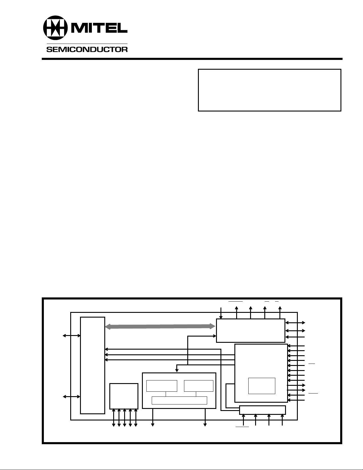
Figure 1 - Functional Block Diagram
RBC R/W1 R/W2
External Memory
Access Control
Timing
Generation
Analog
PLL
Mode Control
OEser
MD2
P0
•
•
P7
WBC
SCLK
HC4
C16C16+
F0i
PCLK
PLLVSS
LP1,LP2
PLLAGND
CKout
RST
PLLVDD
MD0MD1
2-145
Page 2
MT90210 Preliminary Information
A3
VSS
A2
S7
A1
VSS
S8S4S9
VSS
VDD
100 PIN PQFP
S11
S10
S12
S13
VSS
S14
S15
A6
A7
VSS
A8
A9
VDD
A10
VSS
A11
A12
RBC
VDD
VSS
WBC
S0
S1
S2
VSS
VDD
S3
82
84
86
88
90
92
94
96
98
100
A5
VSS
S5
VDD
S6
A4
VDD
P5
P6
P7
Strobe
A0
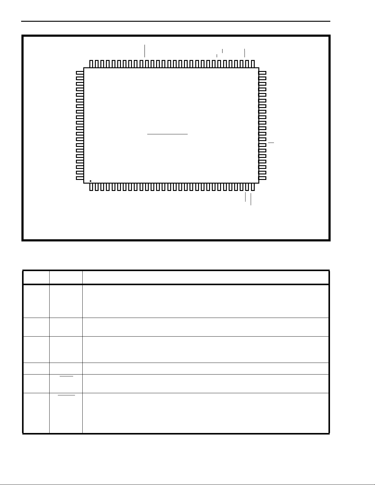
Note: the PQFP package meets the JEDEC standard MO-108, CC1.
Critical dimensions:
Lead pitch = 0.65mm,
Body Size = 14mm x 20mm,
Package size = 17.9mm x 23.9mm.
VSS
VDD
P4
VSS
VDD
S16
/W2
VSS
R
P0
P1
P2
P3
22 24 26 28 30
2018161412108642
S17
S18
S19
S20
S21
VSS
1
W
R/
S22
out
VDD2
CK
S23
TDO
PCLK
RST
525456586062646668707274767880
VSS2
50
48
46
44
42
40
38
36
34
32
RDin
VDD
PLL
PLLAGND
LP1
LP2
PLLVSS
IDDTN
TD
VSS2
C16C16+
VDD2
MD0
MD1
MD2
F0i
TRST
TCK
TMS
TDI
HC4
SCLK
OEser
Figure 2 - Pin Connections
Pin Description
Pin Name Description
95-97,
100,
1-3,
6
7-9,
11-15
18-22,
24-26
27 TDO Boundary Scan Test Data Output.
29 RDin Read P0-P7 input clock. This input is used by the MT90210 to sample b ytes coming in at
30 OEser Serial Port Output Enable (Input). On the parallel-to serial conv ersion direction, this input
S0-S2,
S3,
S4-S6,
S7
S8-S10,
S11-S15
S16-S20
S21-S23
Serial Lines 0-7 (TTL compatible with internal pullups in the range 25 - 125kΩ).
Bidirectional, time division multiplexed serial streams. According to mode selected by
MD0-2 inputs, distinct data rates can be selected at the serial port. In mode 3, these lines
are configured as inputs only. In modes 1, 2, 4 and 5, these lines become bidirectional.
Serial Lines 8-15. See description for S0-S7 above. In mode 3, S8-S11 are inputs and
S12-S15 are outputs. In modes 1, 2, 4 and 5 these are bidirectional lines.
Serial Lines 16-23. See descripton for S0 - S7 above . F or mode 3, these lines are outputs
and operate at 8.192 Mb/s rates. When operating in modes 1, 2, 4 and 5, these lines are
bidirectional.
the parallel port P0-P7 lines. Typically, the user should connect CKout to this input.
is used by the MT90210 to know which time-slots on the serial output streams will be
placed in high-impedance. This input is sampled synchronously along with the parallel
input data before the parallel-to-serial conversion takes place. When low, output serial
channels are actively driven. When set high, the output bus drivers are disabled.
2-146
Page 3

Preliminary Information MT90210
Pin Description (continued)
Pin Name Description
31 SCLK Serial Port Clock (input). The SCLK clock is used to control the serial port operation in
modes 1,2,3 and 4. Depending on the operation mode selected at the MD0-MD2 inputs,
this input can accept 4.096 (MD2-0=000), 8.192 (MD2-0=001) or 16.384 (MD2-0 =010 and
011) MHz clock. In mode 5, this input is ignored.
32 HC4 H-MVIP C4. This is a 4.096 MHz clock utilized in modes 4 and 5 to maintain compatibility
with existing MVIP-90 systems. It is utilized to sample the fr ame pulse input (F0i). Not used
in Modes 1 - 3.
33 TDI Boundary Scan Test Data Input.
34 TMS Boundary Scan Test Mode Select.
35 TCK Boundary Scan Test Clock.
36 TRST Boundary Scan Test Reset.
37 F0i Frame Synchronization Signal (TTL compatible input). This input signal establishes
the frame boundary for the serial input/output streams.
38-40 MD2-MD0 Operation Mode Bits 0-2 (Input). Selects the data rate for the time division, multiplexed
serial streams. 2.048 (mode 1, MD2-0=000), 4.096 (mode 2, MD2-0=001) or 8.192 (mode
3, MD2-0=010) Mb/s data rates are available. When MD2-0 are set to 011 (mode 4), the
MT90210 operates in mixed data rates mode where S16-23 operate at 8.192 Mb/s and the
remaining serial streams run at 2.048 Mb/s. In mode 5 (MD2-0=100), the MT90210
operates as per mode 4 but the device will accept a differential clock reference at 16.384
MHz at pins C16+ and C16-.
42 C16+ Serial P ort Clock Input.In mode 5 (MD2-0= 100), this is a 16.384 MHz diff erential signal.
Note used in Modes 1 - 3.
43 C16- Serial Port Clock Input. The complement to C16+.
45 TD Reserved - Do not connect.
46 IDDTN Connect to Ground.
47 PLLVSS PLL Ground Input.
48 LP2 Loop Filter Input. An external RC circuit is required at this input, refer to Figure 10.
49 LP1 Loop Filter Input. An external RC circuit is required at this input, refer to Figure 10.
50 PLLAGND PLL Analog Ground output. Provides ground to PLL loop filter, refer to Figure 10.
51 PLLVDD PLL Power Input. +5V
52 RST RESET. A low on this pin resets the device.
53 PCLK Parallel Port Clock Input. CKout must be connected to this input.
54 CKout Internal VCO Output Signal. Output of internal PLL frequency multiplier. In mode 1 the
frequency is 16.384 MHz, for the other modes the frequency is 32.768 MHz. Must be
connected to PCLK only.
56 R/W1 Read/Write Output 1. This output signal toggles low for the last half of a memory write
cycle indicating valid data.
57 R/W2 Read/Write Output 2. This output is low f or memory read operations and high for memory
write operations.
2-147
Page 4

MT90210 Preliminary Information
Pin Description (continued)
Pin Name Description
58-59,
61-62,
64,
66-68
70 Strobe Strobe Output. This output is typically connected to the Chip-enable input of the external
72-73,
75- 77,
80-82,
84-85,
87,
89-90
91 RBC Read Data Block Complete (output). A transition on this output is used to notify the
94 WBC Write Data Block Complete (Output). A transition on this output is used to notify the
P0-P1,
P2-P3,
P4,
P5-P7
A0-A1,
A2-A4,
A5-A7,
A8-A9,
A10,
A11-A12
Parallel Input/Output Data Bus. This 8 bit data bus is a bidirectional parallel port used to
perform 8-bit transactions between the MT90210 and the external dual port RAM. Data is
clocked in and out of the P0-P7 parallel port according to Figures 22 and 23.
dual port RAM. It is kept low during all read cycles, stays high during inactive periods and
goes low for the last half of a memory write cycle.
External Memory Address Outputs A0-A12. These 13 address output lines are provided
by the MT90210 to allow a direct connection to an external dual port RAM.
external CPU that the MT90210 has finished reading the contents of one entire 125µs
frame from the external dual port memory (e.g.; from addresses 0000h to 0FFFh in modes
3, 4 or 5). Whenever RBC toggles , the MT90210 starts reading the next half of the memory
(addresses 1000h to 1FFFh) while the local CPU updates the first half with more data to
be sent. RBC toggles every 125µs. When this signal is low, the MT90210 is reading the
lower memory block.
external CPU that the MT90210 has finished writing the contents of one entire 125µs
frame into the external dual port memory (e.g; from addresses 0000h to 0FFFh in modes
3,4 or 5). Once WBC toggles, the local CPU can access the Dual port memory to get the
data while the MT90210 writes the contents of the next 125µs frame into the other half
(addresses 1000h to 1FFFh) of the dual port memory. WBC toggles every 125µs. When
this signal is low, the MT90210 is writing to the lower memory block.
4,16,
63, 71,
78, 86,
92, 99
41, 55 V
5,10,
17, 23,
60, 65,
69, 74,
79,83,
88, 93,
98
28 V
V
V
DD
DD2
SS
SS2
Supply Input. +5V.
Supply Input. +5V.
Ground.
Ground.
2-148
Page 5

Preliminary Information MT90210
Functional Description
The MT90210 is a 100-pin device that converts
incoming serial telecom streams of 2.048, 4.096 or
8.192 Mb/s on to an 8-bit parallel bus, and converts
input data on this parallel bus to the outgoing serial
telecom links. The device is configured to perform
simultaneous parallel-to-serial and serial-to-parallel
conversion.
MT90210 interfaces up to 24 bidirectional serial data
streams to a byte oriented parallel port for access by
a dual-port RAM. It contains an address generator
for parallel port read and write operations directly to
an external dual port memory. A single MT90210
device can handle up to 3072 channels, 1536 on the
transmit and 1536 on the receive direction.
Depending on the operation mode selected at the
mode pins (MD0-MD2), the 64 kb/s serial telecom
channels may be configured as inputs or outputs.
The data on the parallel bus is in a format suitable for
interfacing with popular dual port memories.
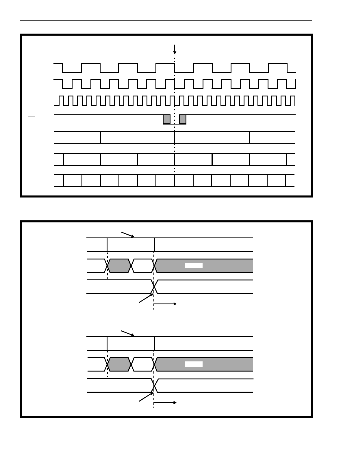
Depending on the data rate selected by the MD0MD2 input pins, serial data is clocked in and out on
the serial streams at either 2.048, 4.096 or 8.192
Mb/s, as shown in Figure 6. A mechanism for
implementing external double buffering is provided
by the Write Block Complete (WBC) and Read Block
Complete (RBC) output pins. Double buffering the
data allows the processor to independently access
an entire frame of data in the external memory while
the MT90210 reads or writes the complementary
frame in the memory. For e xample , in mode 3 (Figure
4), during the first frame the MT90210 will read and
write in to the first half of the memory space (Block
0) and during the second frame the MT90210 will
read and write in to the second half of the memory
space (Block 1). Within each block the transmit data
and receive data are separated and located at fixed
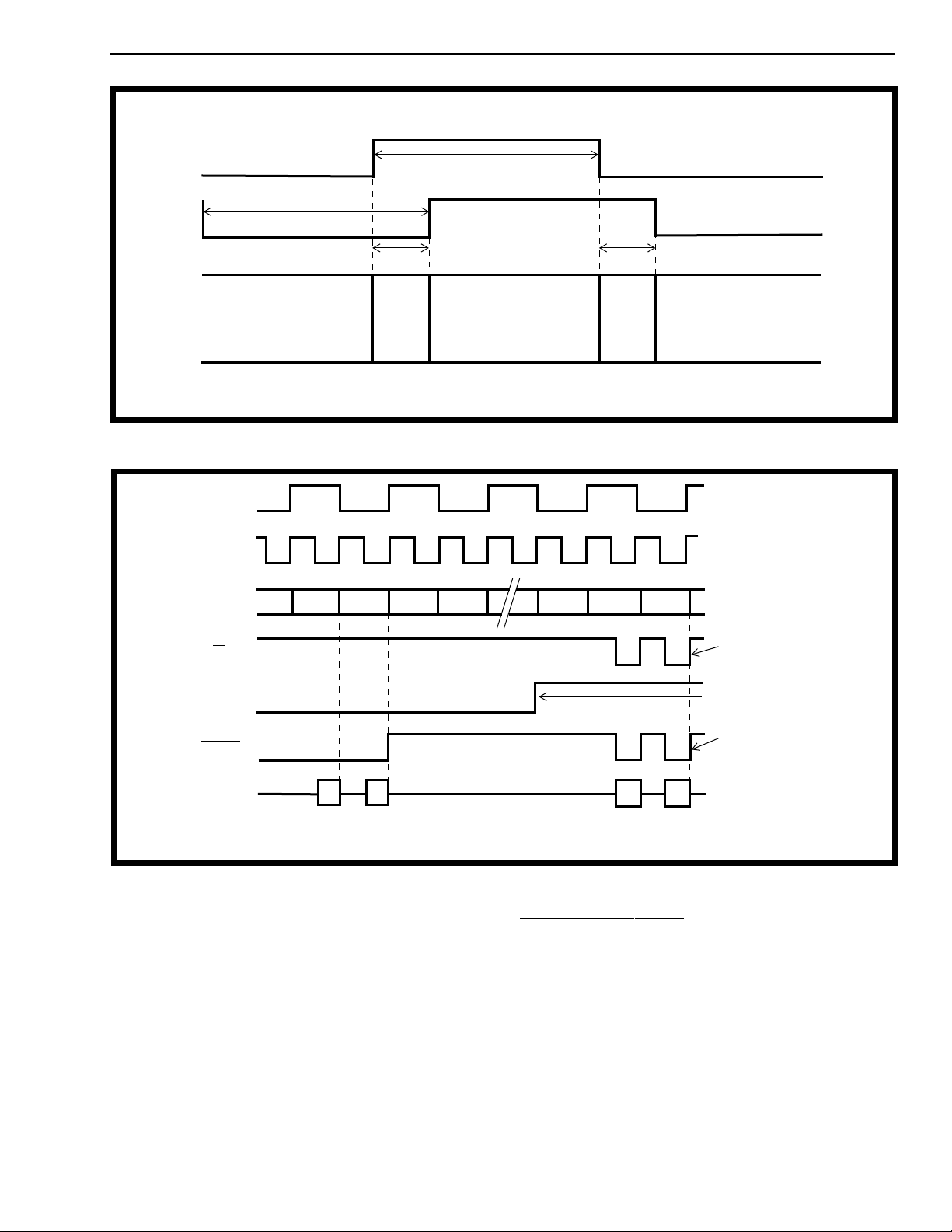
address locations. The operation of WBC and RBC is
shown in Figures 7a and 7b.
On the external memory port side, the device
performs 8-bit wide operations with a cycle time of
30 or 61 ns. The parallel port operates at 16.384
MByte/s (for mode 1) or 32.768 MByte/s (for modes
2,3,4 and 5). To create the high speed clock required
to manage the byte operations at the parallel port, a
built in PLL multiplies the serial port input clock
(SCLK) by a factor of two or four depending on the
mode. In all operation modes, the user should
connect the PLL CKout to PCLK input.
A separate input pin, Output Enable serial (OEser
pin 30), may be used to selectively tristate individual
64Kb/s serial links. By using a 9-bit external dual
port RAM and connecting the ninth bit to OEser as
shown in Figure 9, the processor may disable an
individual channel by setting the ninth bit for that
channel in the transmit (TX) portion of the current
block. The remaining 8 bits for this channel may be
any value since they are ignored by the MT90210
when the ninth bit is 1. To avoid contention on the
serial bus, it is recommend that the user configure all
serial streams as inputs at start-up. This may be
done by setting all OEser bits to 1 in the TX por tions
of both memory blocks. In mode 3, the serial streams
are permanently configured as 12 inputs and 12
outputs, and the state of OEser is ignored.
An Overview of CTI bus protocols
Multi-Vendor Integration Protocol (MVIP) provides a
coherent approach to building solutions for
worldwide markets by merging computing and
communications technologies under one open
architecture. MVIP ensures inter-operability among
telephone-based resources (such as trunk
interfaces, voice, video, fax, text-to-speech, speech
recognition) for use within a computer chassis in an
individual or networked configuration. H-MVIP
addresses the need for higher telephony traffic
capacity in individual computer chassis. H-MVIP
defines three major items that together make a
useful digital telephony transport and switching
environment: the H-MVIP digital telephony bus with
up to 3072 "time-slots" of 64 Kb/s each; a bus
interface with digital switching that allows a group of
H-MVIP interfaced circuit boards to provide
complete, flexible, distributed telephony switching;
and a logical device driver model and standard
software interface to a logical model.
Operating Modes
The MT90210 device can operate in one of five
modes appropriate for different application needs.
Mode selection must be done while the device is in
reset (RST low and a valid clock applied to the PCLK
input). These modes are explained in the following
paragraphs.
Mode 1: The serial input/output format conforms to
the ST-BUS requirements when the data rate is
2.048 Mb/s (see Figure 6). Serial port clock (SCLK)
is 4.096 MHz. The on-chip PLL produces a phase
locked 16.384 MHz clock (CKout) from the SCLK
input. In this data rate operation, the 24 serial lines
(S0-23) become bidirectional links at 2.048 Mb/s.
The ST-BUS is a time-division multiplexed serial bus
with 32, 8-bit channels per frame. Frame boundaries
are delineated by the frame pulse. Figure 3 depicts
2-149
Page 6
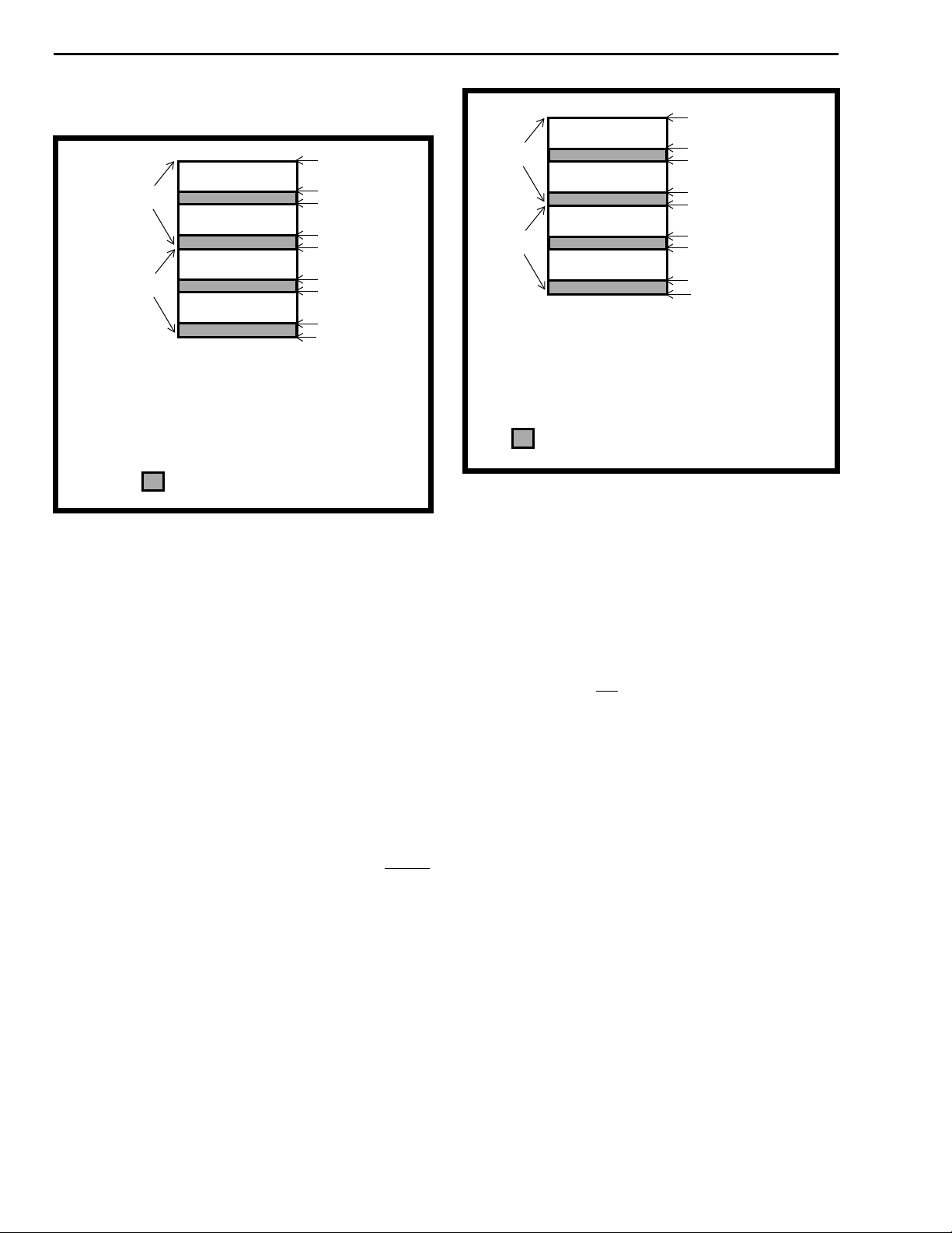
MT90210 Preliminary Information
how the data from the serial port is mapped into the
external dual port memory.
768 bytes
for TX
BLOCK 0
BLOCK 1
24 bidirectional streams at 2.048Mb/s
768 bytes
for RX
768 bytes
for TX
768 bytes
for RX
MODE 1
0000
02FF
0400
06FF
0800
0AFF
0C00
0EFF
0FFF
1536 bytes
for TX
BLOCK 0
BLOCK 1
24 bidirectional streams at 4.096Mb/s,
or 12 in / 12 out at 8.192Mb/s
Address outputs used: A0-A12
1536 bytes
for RX
1536 bytes
for TX
1536 bytes
for RX
MODES 2 & 3
0000
05FF
0800
0DFF
1000
15FF
1800
1DFF
1FFF
Address outputs used: A0-A11;
A12 always zero.
Legend:
unused memory space
Figure 3 - Dual Port RAM Memory Map for
Mode 1
Mode 2: When the device is configured for
4.096 Mb/s data rate operation, each of the 24 timedivision multiplexed serial streams is made up of 64
channels. In this data rate operation, the 24 serial
lines (S0-23) become bidirectional links at
4.096 Mb/s. Serial por t clock (SCLK) is 8.192 MHz.
The on-chip PLL produces a phase locked 32.768
MHz clock (CKout) from the SCLK input. Figure 4
depicts how the data from the serial port is mapped
into the external dual port memory.
Mode 3: When the device is configured for 8.192
Mb/s data rate operation, each of the 24 timedivision multiplexed serial streams is made up of 128
channels. In this mode, bidirectional operation on the
serial port streams is not provided and the MT90210
is set in a 12 in / 12 out configuration and the OEser
input is ignored. Streams S0-S11 are configured as
inputs, and S12-S23 are configured as outputs.
Serial port clock is 16.384 MHz. The on-chip PLL
doubles this clock to produce a CKout clock of
32.768 MHz. Figure 4 depicts how the data from the
serial port is mapped into the external dual port
memory. Figure 12 and Table 3 show the write and
read operations on the parallel port at the frame
boundary.
Legend:
unused memory space
Figure 4 - Dual Port RAM Memory Map for
Modes 2 and 3
Mode 4: The MT90210 is configured such that the
24 serial streams are bidirectional and split into two
different functional groups: (i) streams S0-S15
operate at 2 Mb/s rate (512 timeslots), (ii) S16-S23
operate at 8.192 Mb/s rate (1024 timeslots). Memory
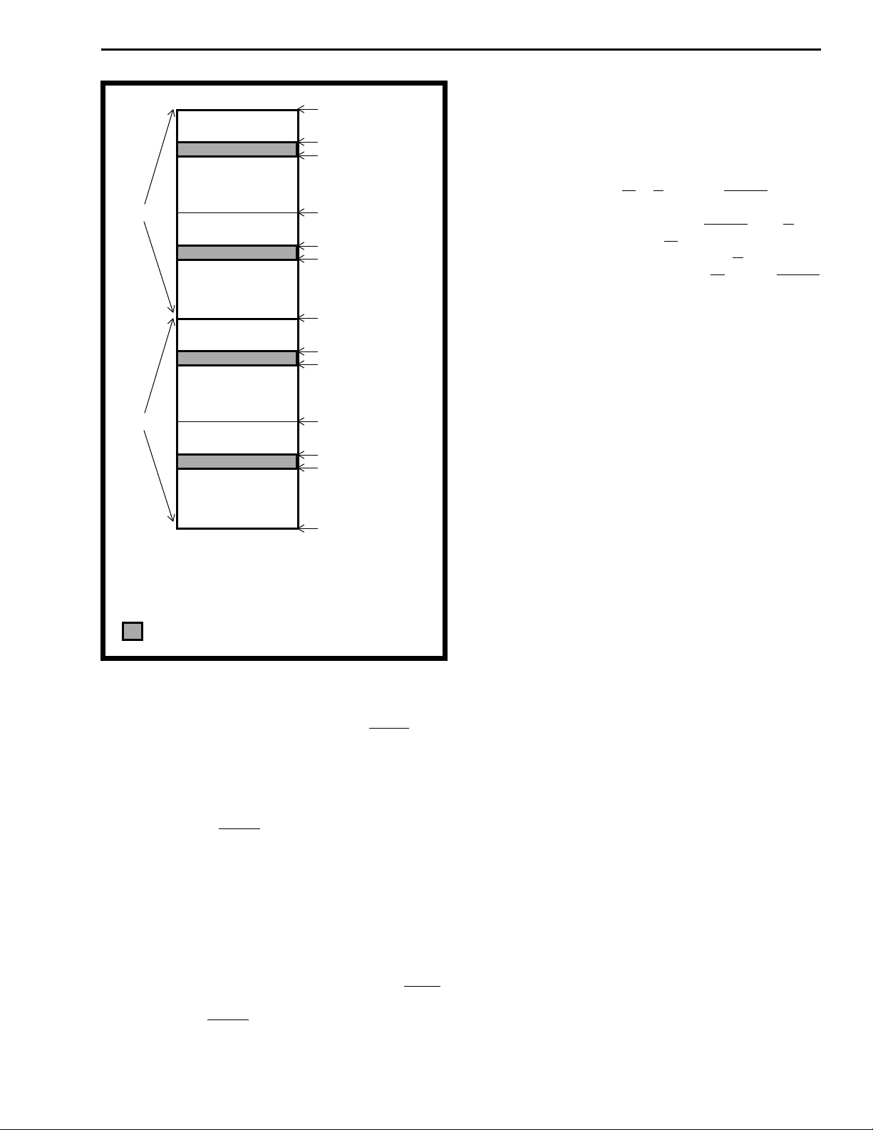
mapping for mode 4 is described in Figure 5. For
compatibility with legacy MVIP timing, mode 4
provides an additional clock input at 4.096 MHz
(HC4 input pin) which allows the device to detect
frame sync pulse (F0i) with a typical width of 244 ns.
In mode 4, the 16.384 (SCLK) and 4.096 (HC4) MHz
clocks should be in sync according to H-MVIP
specifications. The on-chip PLL doubles SCLK to
produce a CKout signal of 32.768 MHz. Figure 13
and Table 4 show the write and read operations on
the parallel port at the frame boundary.
Mode 5: Identical operation as per mode 4 with the
difference that the 16.384 MHz clock is a differential
signal received at the two input pins, C16+ and C16of the MT90210 device. The differential clock is
needed to eliminate distortion in the clock signal
passing through a ribbon cable as per H-MVIP
specification. The SCLK input is not used in this
mode. Memory mapping for mode 5 is depicted in
Figure 5.
2-150
Page 7
Preliminary Information MT90210
Functional operation of the MT90210
512 bytes for
S0-S15 TX
1024 bytes for
S16-S23 TX
BLOCK 0
BLOCK 1
S0-S15 bidirectional 2.048Mb/s streams
S16-S23 bidirectional 8.192Mb/s streams
Address outputs used: A0-A12
Legend:
unused memory space
512 bytes for
S0-S15 RX
1024 bytes for
S16-S23 RX
512 bytes for
S0-S15 TX
1024 bytes for
S16-S23 TX
512 bytes for
S0-S15 RX
1024 bytes for
S16-S23 RX
0000
01FF
0400
0800
09FF
0C00
1000
11FF
1400
1800
19FF
1C00
1FFF
Figure 5- External Double Buffer Operation and
Memory Arrangement in Modes 4 and 5.
Bidirectional Operation: Serial output channel
timeslots can be tri-stated by setting the OEser input
pin high during a specific parallel channel timeslot.
Note that when operating in bidirectional mode, the
MT90210’s I/O buffers on the serial port are
permanently at high impedance and the control of
contention on the serial bus has to be done by the
user through the OEser input pin. In modes 1, 2, 4
and 5 all of the transmit channels on the serial port
side are copied back to the memory interface. This is
true only in bidirectional modes (i.e., modes 1, 2, 4
and 5). Note that only the transmit (output) channels
are copied back to the memory and that the input
channels remain unaffected.
For a specific time-slot sampled at the external
memory parallel interface, the respective OEser
input pin must be in the desired state; i.e., the
sampling of the OEser input is synchronized with the
parallel byte read at the P0-P7 lines.
device at the parallel interface for
modes 1, 2, and 3
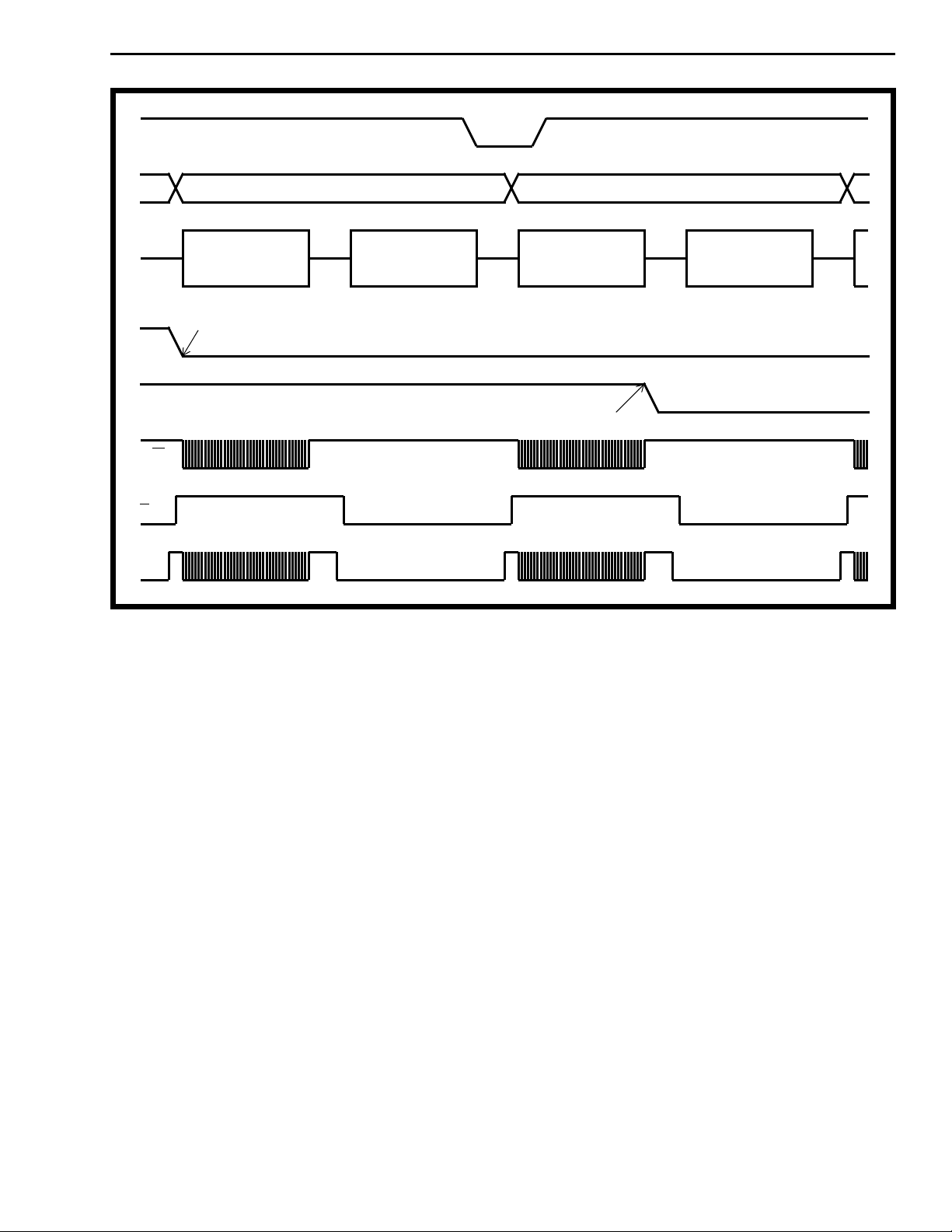
Figures 8, 12, and 13 depict the parallel port READ
and WRITE operation of the MT90210 device. The
state of the signals R/W1, R/W2 and Strobe defines
a valid Read or a valid Write operation. During a
valid READ operation the signals Strobe and R/W2
stay LOW while the signal R/W1 is always HIGH. For
the valid WRITE operation the signal R/W2 always
stays HIGH while the signals R/W1 and Strobe
toggle. Table 3 represents the sequence of events as
depicted in Figure 12 during the last channel at the
end of an ST-BUS frame. The MT90210 device
repeats the same sequence of operation during the
entire frame. For example, during channel 127 at the
end of an ST-BUS frame the MT90210 will write
channel 126 (streams 0 to 11) and read from channel
1 (streams 12 to 23) of the next frame as shown in
Table 3. Note that there is a two channel difference
between a write and a read sequence. In mode 1
and mode 2, the MT90210 device performs a group
of writes and a group of reads separated by 8 PCLK
periods, while for modes 3, 4 and 5 they are
separated by 4 PCLK periods.
Functional operation of the MT90210
device at the parallel interface for mode
4 and mode 5
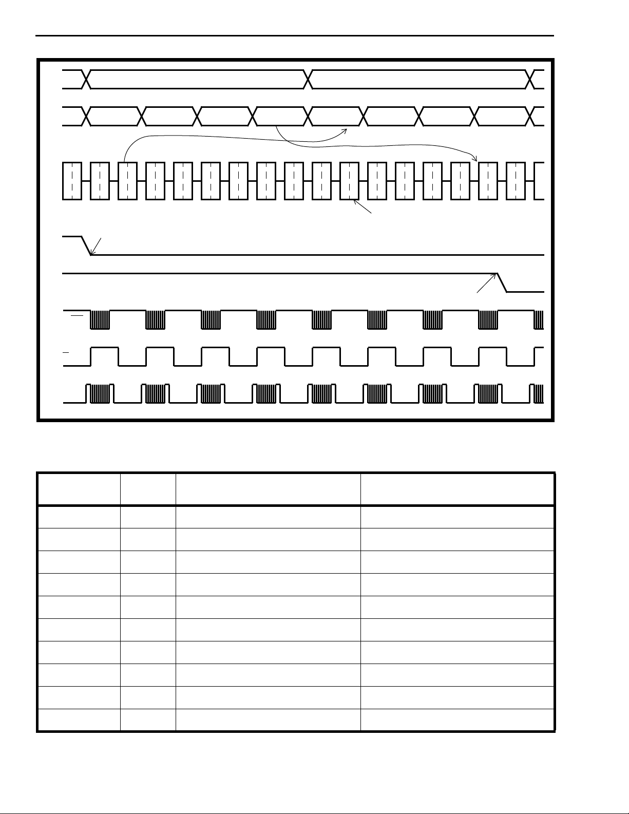
Table 4 represents the sequence of events when the
MT90210 device is operating at a mixed rate of
operation (mode 4 and mode 5) as depicted in Figure
13. The MT90210 device repeats the same sequence
of operation as shown in Table 4 throughout the entire
frame. In mode 4 and mode 5 the MT90210 device is
configured with 24 bidirectional serial streams and split
into two different rates: S0 to S15 operate at 2.048
Mb/s data rates (512 time-slots) and streams S16 to
S23 run at 8 Mb/s data rates (1024 time-slots). In this
mode, 12 writes are carried out during a parallel port
write cycle and 12 reads during a read cycle. Of each
group of 12, 8 are dedicated to the high-speed 8.192
Mb/s links, therefore four slots are available for the
2.048 Mb/s links. To process all the 16 streams
devoted for 2.048 Mb/s, four separate write or read
cycles are required (these slots are denoted with the
suffix "a", "b", "c", "d" in Figure 13). Each write or
read cycle will use four time-slots. For example, read
or write cycle "a" uses streams S0 to S3, read or
write cycle "b" uses streams S4 to S7, read or write
cycle "c" uses streams S8 to S11 and read or write
cycle "d" uses streams S12 to S15 (see Table 4).
There is a two channel difference between a read
and write sequence for 2 Mb/s data and an eight
channel difference for 8 Mb/s data.
2-151
Page 8
MT90210 Preliminary Information
Frame Boundary Established by F0i
SCLK
(4 MHz)
SCLK
(8 MHz)
SCLK, C16
(16 MHz)
F0i
Serial I/O
2 Mb/s
Serial I/O
4 Mb/s
Serial I/O
8 Mb/s
W
R
I
T
E
Ch. 31, Bit 1
Ch. 63, Bit 2 Ch. 63, Bit 1 Ch. 63, Bit 0 Ch. 0, Bit 7 Ch. 0, Bit 6 Ch. 0, Bit 5
Ch. 127,
Bit 5
Ch. 127,
Bit 4
Ch. 127,
Bit 3
Ch. 31, Bit 0 Ch. 0, Bit 7 Ch. 0, Bit 6
Ch. 127,
Bit 2
Ch. 127,
Bit 1
Ch. 127,
Bit 0
Ch. 0,
Bit 7
Ch. 0,
Bit 6
Ch. 0,
Bit 5
Ch. 0,
Bit 4
Figure 6 - Serial Port Functional Timing
last write address
of frame n
A0-A12
P0-P7
WBC
Data
Out
address x
Data
Out
inactive
inactive
Ch. 0,
Bit 3
Ch. 0,
Bit 2
2-152
MT90210 finishes writing
data from frame n.
last read address
of frame n
R
E
A
A0-A12
P0-P7
Data
In
address y
Data
In
MT90210 will handle parallel port
transactions related to frame n +1.
inactive
inactive
D
WBC
MT90210 finishes reading
data from frame n.
MT90210 will handle parallel port
transactions related to frame n +1.
Figure 7a - WBC and RBC Output Transition
Page 9
Preliminary Information MT90210
RBC
125 us
WBC
Exclusive access of
Block 0
125 us
t
NA
Access
of both
Block 0
&
Block 1
Exclusive access of
Block 1
t
NA
Access
of both
Block 0
&
Block 1
tNA ~ 1 timeslot for modes 1, 2 & 3
tNA ~ 3 timeslots for modes 4 & 5
Exclusive access of
Block 0
Figure 7b - WBC and RBC operation in relation to accessing data from Block 0 and Block 1
SCLK
PCLK
A0-A12
R/
W1
R/W2
Strobe
A
RD
A
RD
A
WR
A
WR
Toggles only during
write data cycle
Changes state (high to low)
on every change of a block
of reads or block of writes
Low during read cycle,
high during inactive
periods and toggles
during write cycles
P0-P7
Note: The MT90210 device performs groups of writes and groups of reads separated by 4 inactive PCLK periods
for modes 3, 4 and 5. In mode 1 and mode 2, the write and read groups are separated by 8 PCLK periods.
RD RD
WR
WR
Figure 8 - Parallel Port Functional Read/Write Operation
JTAG Support
Test Access Port (TAP)
The Test Access Port (TAP) provides access to many
The MT90210 JTAG interface is designed according
to the Boundary-Scan standard IEEE1149.1. The
standard specifies a design-for-testability technique
called Boundary-Scan Test (BST). A boundary-scan
IC has a shift-register stage or ‘Boundary-Scan Cell’
(BSC) in between the core logic and the I/O buffers
adjacent to each I/O pin. The BSCs can control and
observe what happens at each I/O pin of the IC. The
operation of the boundary-scan circuitry is controlled
test support functions built into the MT90210. It
consists of three input connections and one output
connection. The following connections form the TAP:
• Test Clock Input (TCK)
• Test Mode Select Input (TMS)
• Test Data Input (TDI)
• Test port Reset (TRST)
• Test Data Output (TDO)
by a Test Access Port (TAP) Controller.
2-153
Page 10

MT90210 Preliminary Information
I[0:1] Instruction Description
[00] EXTEST Boundary-Scan
register selected,
Test Enabled
This instruction is specifically provided to allow board-level interconnect
testing of opens, bridging errors etc.
When the EXTEST instruction is selected, the on-chip logic is isolated
from the MT90210’s I/O pin such that the value of the I/O pins is
determined by its boundary-scan register. Data for the execution of this
instruction can be preloaded into the boundary-scan register with the
SAMPLE/PRELOAD instruction.
[01],
[10]
SAMPLE/
PRELOAD
Boundary-Scan
register selected,
Test Disabled
Two functions can be performed by the use of this instruction. It allows a
SAMPLE (‘snapshot’) of the normal operation of the MT90210 to be
taken for examination. And, prior to the selection of another test
operation, a PRELOAD can place data values into the latched parallel
outputs of the Boundary-Scan cells. During the execution of the
instruction, the on-chip logic operation is not hampered in any way.
[11] BYPASS/
NOTEST
Bypass register
selected,
Test Disabled
This instruction is used to BYPASS the MT90210 while performing
boundary-scan testing on other devices with scan registers in the same
serial register chain. The MT90210 is allowed to function normally. This
instruction is automatically loaded upon reset of the MT90210, as
specified in IEEE1149.1
Table1 - Instruction Register
Instruction Register
In accordance with the IEEE 1149.1 standard, the
MT90210 uses public instructions listed in Table 1.
The MT90210 JTAG Interface contains a two bit
instruction register. Instructions are serially loaded
into the Instruction Register from the TDI when the
TAP Controller is in its Shift-IR state. Subsequently,
the instructions are decoded to achieve two basic
functions: to select the test data register that may
operate while the instruction is current and to define
the serial test data register path that is used to shift
data between TDI and TDO during data register
scanning.
Bits Definition BSC Type
1:60 S4 - S23 B
61 RDIN I
62 OEser I
63 SCLK I
64 HC4 I
65 F0i I
66:68 MD2 - MD0 I
69 RST I
†
Test Data Registers
As specified in the IEEE 1149.1 Standard, the
MT90210 JTAG interface contains two test data
registers:
• The Boundary Scan Register
• The Bypass Register
The MT90210 boundary-scan register contains 144
bits. Bit 144 in Table 2 is the first bit clocked out. All
tristate enable bits are asserted high: a logic 1
enables the corresponding group of
outputs/bidirectionals. Note that clocking all zeros
into the scan path register will set all outputs to
tristate.
2-154
70 PCLK I
71:72 CKO O
73:76 R/W1 - R/W2 O
77:100 P0 - P7 B
101:102 Strobe O
103:128 A0 - A12 O
129:130 RBC O
131:132 WBC O
133:144 S0 - S3 B
Table 2 - Boundary Scan Register
†
B - bidirectional: input cell, output cell followed by
tristate cell.
I - input: input cell.
O - output: output cell, followed by tristate cell.
Page 11
Preliminary Information MT90210
ST-BUS
SCSA
MVIP
H-MVIP
24
S0-S23
+5V
DUAL PORT RAM*
SEM
L
SEM
+5V
R
Mode 1: 4.096 MHz
Mode 2: 8.192 MHz
Mode 3
& 4: 16.384 MHz
8 kHz
Mode 5: 16.384 MHz
Mode 5: 16.384 MHz
Mode 4 & 5: 4.096 MHz
BOUNDARY
SCAN
CONNECTOR
5
SCLK
F0i
C16+
C16-
HC4
MT90210
TRST
TDI,TDO
TMS,TCK
PLLAGND
LP1
LP2
Strobe
R/W2
OEser
P7-P0
A12-A0
W1
R/
RDin
PCLK
CKout
RST
WBC
RBC
9th bit
CE
L
OE
L
External
9
13
+5V
I/O8L-I/O
A
12L-A0L
W
R/
L
MS
0L
CE
R
OE
R
I/O8R-I/O
0R
A
12R-A0R
13
R/W
R
Interface to PC Bus
and/or hardware control
9
for monitoring purpose
MD0
MD1
MD2
* Note: Dual Port RAM: Cypress part number: CY7B145-15 and IDT part number IDT7015
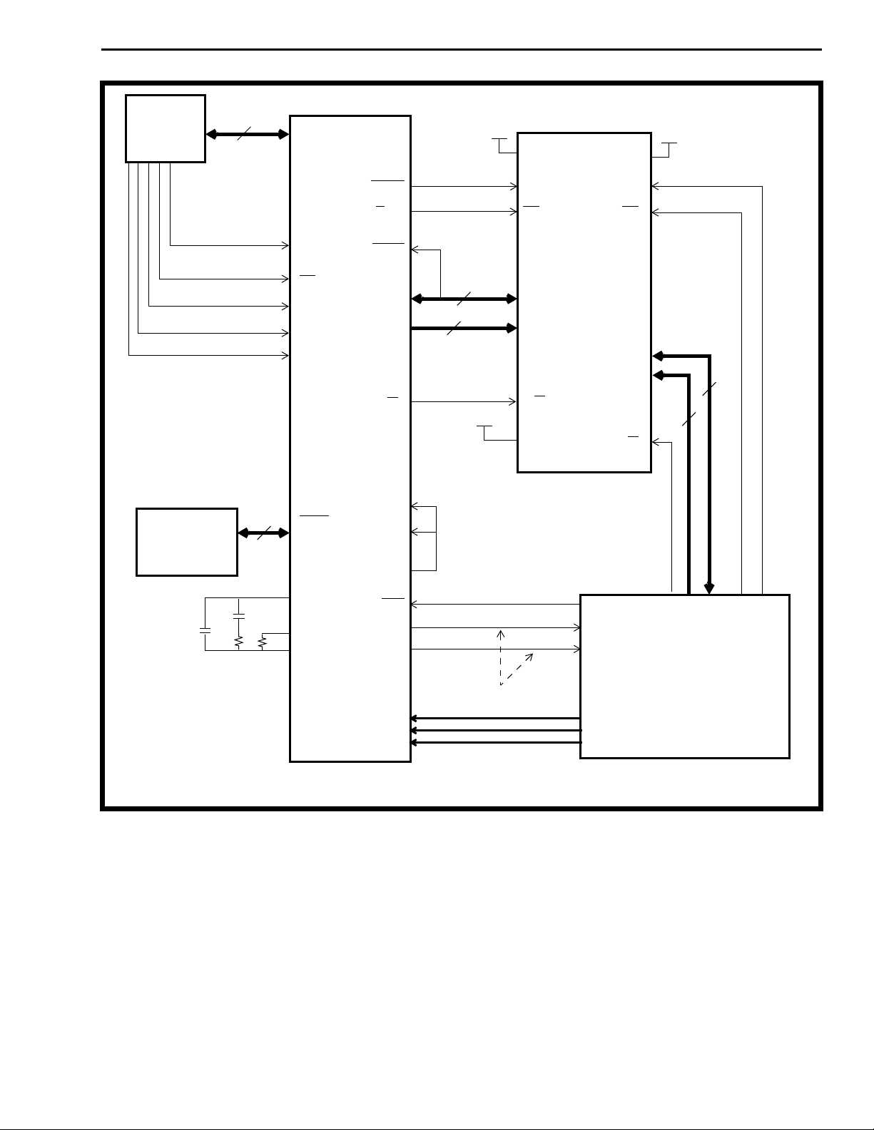
Figure 9 - Functional Example of the MT90210 Application Circuit
Applications
provided by the MT90210: (i) the 24/2 mode in which
all 24 lines operate at 2.048 Mb/s and (ii) the mixed
rate of operation in which 16 streams operate at
The MT90210 device may be used in applications
such as video and teleconferencing bridge cards and
voice processing cards for CTI (Computer Telephony
Integration). MT90210 transfers all TDM channels of
the ST-BUS interface into an external buffer. This
eliminates long answer time and permits fast DSP
access to ST-BUS, SCSA, MVIP or H-MVIP serial
2.048 Mb/s and the remaining 8 streams operate at
8.192 Mb/s data rates. When operating at 8.192
Mb/s rates, the MT90210 automatically terminates
the C16+ and C16- differential clocks specified by
the H-MVIP specifications. Figure 9 shows a
functional block diagram of the MT90210 in a typical
application.
TDM buses. The MT90210 component can be set in
H-MVIP mode with 24 fully bidirectional serial
streams that are configured in different data rate
combinations. Two data I/O subsets of H-MVIP are
(Customer Specific Control
Logic)
2-155
Page 12
MT90210 Preliminary Information
PLLAGND
C1
LP1
MT90210
R1
LP2
R1= 3kΩ
R2= 100Ω + 5%
C1= 10nF
C2= 20pF
+ 5%
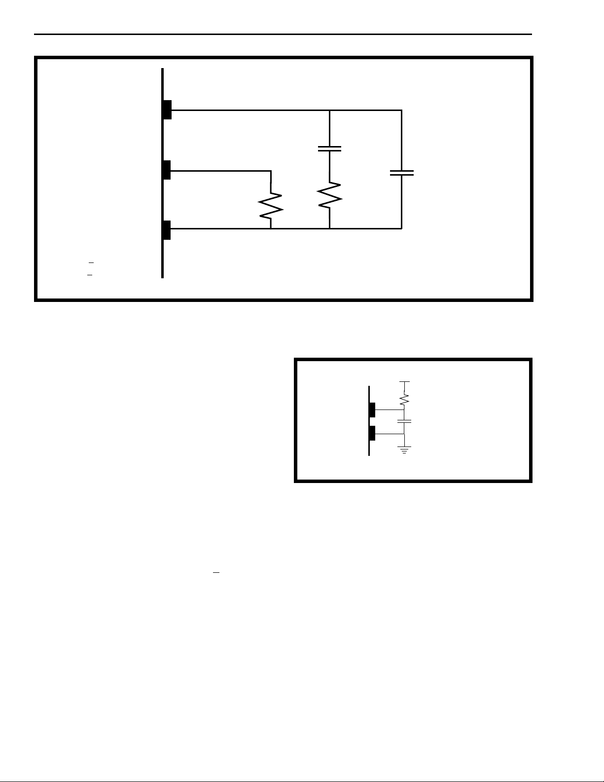
Figure 10 - Analog PLL Low Pass Filter Circuit
PLL Considerations
The MT90210 device contains an analog PhaseLocked Loop (PLL) which is used to create a higher
speed clock for parallel port operation from the input
SCLK. This analog PLL requires a loop filter circuit to
be connected to the LP1 and LP2 pins, as shown in
Figure 10. Additionally, the following design
considerations are recommended for the PLL
circuitry:
R2
PLLVDD
PLLVSS
MT90210
C2
+5V
100Ω
1.0nF
• Phase tolerance and jitter are independent of
the PLL frequency.
• Jitter is affected by the noise on the PLLVDD
and PLLVSS pins. It will increase if the noise
level increases and is recommended to be kept
less than 10 MHz on PLLVDD.
• Use of a C2 capacitor of 15-25pF (+10%) is
recommended to reduce jitter.
• The components should be connected within
one inch (1") of the package.
• Use a wide PCB trace for PLLVDD and PLL VSS
separate from the device VDD/VSS
connections.
• In some setups, an RC network (Figure 11)
between PLLVDD and PLLVSS supplies helps
to reduce jitter.
2-156
Figure 11 - PLLVDD/PLLVSS RC Circuit
Page 13

Preliminary Information MT90210
PCLK Cycle Read Write Channel Stream Memory Address
1 - wr 126 0 0DE8h
2 - wr 126 1 0DE9h
3 - wr 126 2 0DEAh
4 - wr 126 3 0DEBh
5 - wr 126 4 0DECh
6 - wr 126 5 0DEDh
7 - wr 126 6 0DEEh
8 - wr 126 7 0DEFh
9 - wr 126 8 0DF0h
10 - wr 126 9 0DF1h
11 - wr 126 10 0DF2h
12 - wr 126 11 0DF3h
13 to 16 INACTIVE
17 rd
18 rd - 0 1 1001h
19 rd - 0 2 1002h
20 rd - 0 3 1003h
21 rd - 0 4 1004h
22 rd - 0 5 1005h
23 rd - 0 6 1006h
24 rd - 0 7 1007h
25 rd - 0 8 1008h
26 rd - 0 9 1009h
27 rd - 0 10 100Ah
28 rd - 0 11 100Bh
29 to 32 INACTIVE
Table 3 - Functional Example of the Read and Write Operation (Mode 3)
-
0 0 1000h
2-157
Page 14

MT90210 Preliminary Information
PCLK Cycle Read Write
1 - wr 124 16 - - 0FE0h
8 - wr 124 23 - - 0FE7h
9 - wr - - 31 0 09F0h
10 - wr - - 31 1 09F1h
11 - wr - - 31 2 09F2h
12 - wr - - 31 3 09F3h
13
.
.
16
17 to 24 rd
25 to 28 rd
29 to 32 INACTIVE
33 to 40 - wr 125 16 to 23 - - 0FE8h to 0FEFh
-
-
8Mb/s
Channel
4 16 to 23 - - 0420h to 0427h
- - 1 0 to 3 0010h to 0013h
8 Mb/s
Stream
.
.
INACTIVE
2 Mb/s
Channel
2 Mb/s
Stream
Memory Address
41 to 44 - wr - - 31 4 to 7 09F4h to 09F7h
45 to 48 INACTIVE
49 to 56 rd - 5 16 to 23 - - 0428h to 042Fh
57 to 60 rd - - - 1 4 to 7 0014h to 0017h
61 to 64 INACTIVE
65 to 72 - wr 126 16 -23 - - 0FF0h to 0FF7h
73 to 76 - wr - - 31 8 to 11 09F8h to 09FBh
77 to 80 INACTIVE
81 to 88 rd - 6 16 to 23 - - 0430h to 0437h
89 to 92 rd - - - 1 8 to 11 0018h to 001Bh
93 to 96 INACTIVE
97 to 104 - wr 127 16 to 23 - - 0FF8h to 0FFFh
105 to 108 - wr - - 31 12 to 15 09FCh to 09FFh
109 to 112 INACTIVE
113 to 120 rd - 7 16 to 23 - - 0438h to 043Fh
121 to 124 rd - - - 1 12 to 15 001Ch to 001Fh
Table 4 - Functional Example of the Parallel Interface for Mode 4 and 5
2-158
Page 15
Preliminary Information MT90210
F0i
S23:S0
Frame n, last channel Frame n+1, channel 0
P7:P0
RBC
WBC
R/W1
R/W2
STROBE
Write data from
S23-S0 frame n,
nd
last channel
2
Finished reading last channel of frame n
Read data for
S23-S0 frame n+1,
channel 0
Finished writing last channel of frame n
Figure 12 - Modes 1, 2, 3 Read/Write Timing
Write data from
S23-S0 frame n,
last channel
Read data for
S23-S0 frame n+1,
channel 1
2-159
Page 16
MT90210 Preliminary Information
2M ts Frame n, channel 31 Frame n+1, channel 0
8M ts ch 124 ch 125 ch 126 ch 127 ch 0 ch 1 ch 2 ch 3
P7:P0
R8 127
RBC
WBC
R/W1
R/W2
STROBE
3 channel delay for 8 Mb/s rate
W8 121
W2 30b
R8 1
R2 0b
R2 31d
Finished reading last channel of 8Mb/s
and 4
R8 0
W8 120
R2 0a
W2 30a
th
quarter of last channel of 2 Mb/s of one complete frame(125 us)
Figure 13 - Mode 4 and Mode 5 Read/Write Timing
W8 122
W2 30c
R8 2
R2 0c
W8 123
W2 30d
R8 3
R2 0d
R8 4
W8 124
R2 1a
W2 31a
Finished writing last channel of 8 Mb/s
th
quarter of last channel of 2 Mb/s
and 4
R8 5
W8 125
"a" denotes data for S0-S3
"b" denotes data for S4-S7
"c" denotes data for S8-S11
"d" denotes data for S12-S15
W2 31b
R2 1b
W8 126
R8 6
W2 31c
R2 1c
W8 127
W2 31d
R8 7
R2 1d
Mode TX/RX
Memory Address Location Formula
for Block 0
Memory Address Location Formula
for Block 1
1 TX 24C + S 24C + S + 800h
1 RX 24C + S + 0400h 24C + S + C00h
2 TX 24C + S 24C + S + 1000h
2 RX 24C + S + 0800h 24C + S + 1800h
3 TX 12C + S 12C + S + 1000h
3 RX 12C + S + 0800h 12C + S + 1800h
4 or 5 (@ 2M) TX 16C + S 16C + S + 1000h
4 or 5 (@ 2M) RX 16C + S + 0800h 16C + S + 1800h
4 or 5 (@ 8 M) TX 8C + (S-16) + 0400h 8C + (S-16) + 1400h
4 or 5 (@ 8M) RX 8C + (S-16) + 0C00h 8C + (S-16) + 1C00h
Table 5 - Memory Address Location Formulae for all modes of operation
C = channel number, S = stream number
2-160
Page 17

Preliminary Information MT90210
Absolute Maximum Ratings* - Voltages are with respect to V
unless otherwise stated.
SS
Parameter Symbol Min Max Units
1 DC Power Supply Voltage VDD to V
SS
2 Voltage on any pin (other than supply pins) V
3 Current at any pin (except VDD and VSS)I
4 Package Power Dissipation P
*Exceeding these values may cause permanent damage. Functional operation under these conditions is not implied
Recommended Operating Conditions - Voltages are with respect to ground (V
V
DD
i
O
D
VSS+0.3 VDD+0.3 V
) unless otherwise stated
SS
Characteristics Sym Min Typ Max Units Test Conditions
1 Operating Temperature T
2 Power Supply Voltage V
OP
DD
-40 25 +85 °C
4.75 5.0 5.25 V
6V
40 mA
2mW
DC Electrical Characteristics
†
Characteristics Sym Min Typ* Max Units Test Conditions
1 Supply Current I
2 Input High Voltage, all inputs V
3 Input Low Voltage, all inputs V
4 Specific Output High Sourcing Current I
5 Specific Output Low Sinking Current I
6 Leakage Current
OH
I
DD
IH
OL
LK
2.0 V
IL
0 0.8 V
12 mA VOH=2.4V
12 mA VOL=0.4V
S0-S23
All other pins
7 Pin Capacitance C
† DC Electrical Characteristics are over recommended operating conditions unless otherwise stated.
* Typical figures are at 25°C and are for design aid only.
P
15 100 mA
DD
200
5
10 pF
V
µA
2-161
Page 18
MT90210 Preliminary Information
†
AC Electrical Characteristics
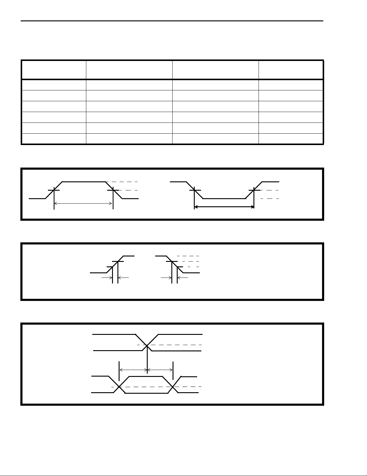
timing specifications. The setup/hold and propagation delays are based on a single reference level which is 1.5V for TTL(VTT) and 0.5*VDD for
CMOS (VCT).
-
The following table specifies voltage reference levels used in both input timing and output
Voltage Reference
V
H
V
HM
V
LM
V
L
V
TT
V
CT
Voltage Value when
Connected to TTL
2.4 0.9*V
2.0 0.7*V
0.8 0.3*V
0.4 0.1*V
Voltage Value when
Connected to CMOS
DD
DD
DD
DD
Units
V
V
V
V
1.5 not applicable V
not applicable 0.5*V
V
H
V
TT
t
V
L
DD
t
V
V
H
V
TT
V
L
Figure 14 - Input Pulse Width
Clock
Input Data
V
H
V
HM
V
LM
V
L
t
t
Figure 15 - Input Rise and Fall Times
V
H
V
TT
V
L
t t
V
H
V
TT
V
L
Figure 16 - Setup Time and Hold Time
2-162
Page 19
Preliminary Information MT90210
V
clock
t
H
V
TT
V
L
drive to drive
output
drive to hiz-low
output
drive to hiz-high
output
F0i
t
t
Figure 17 - Output Delays
t
frw
t
frs
t
frh
V
TT
4.096 MHz (Mode 1)
8.192 MHz (Mode 2)
16.384 MHz (Mode 3)
SCLK
S0-23
(inputs)
S0-23
(outputs)
†
Mode 1, last channel = 31
Mode 2, last channel = 63
Mode 3, last channel = 127
t
clk
t
clkl
t
clkh
t
stis
bit 0, last ch
bit 0, last ch
†
t
stod
†
bit 7, ch.0
Figure 18 - Serial Port Timing for Modes 1, 2, 3
bit 7, ch.0
t
stih
t
T
2-163
Page 20
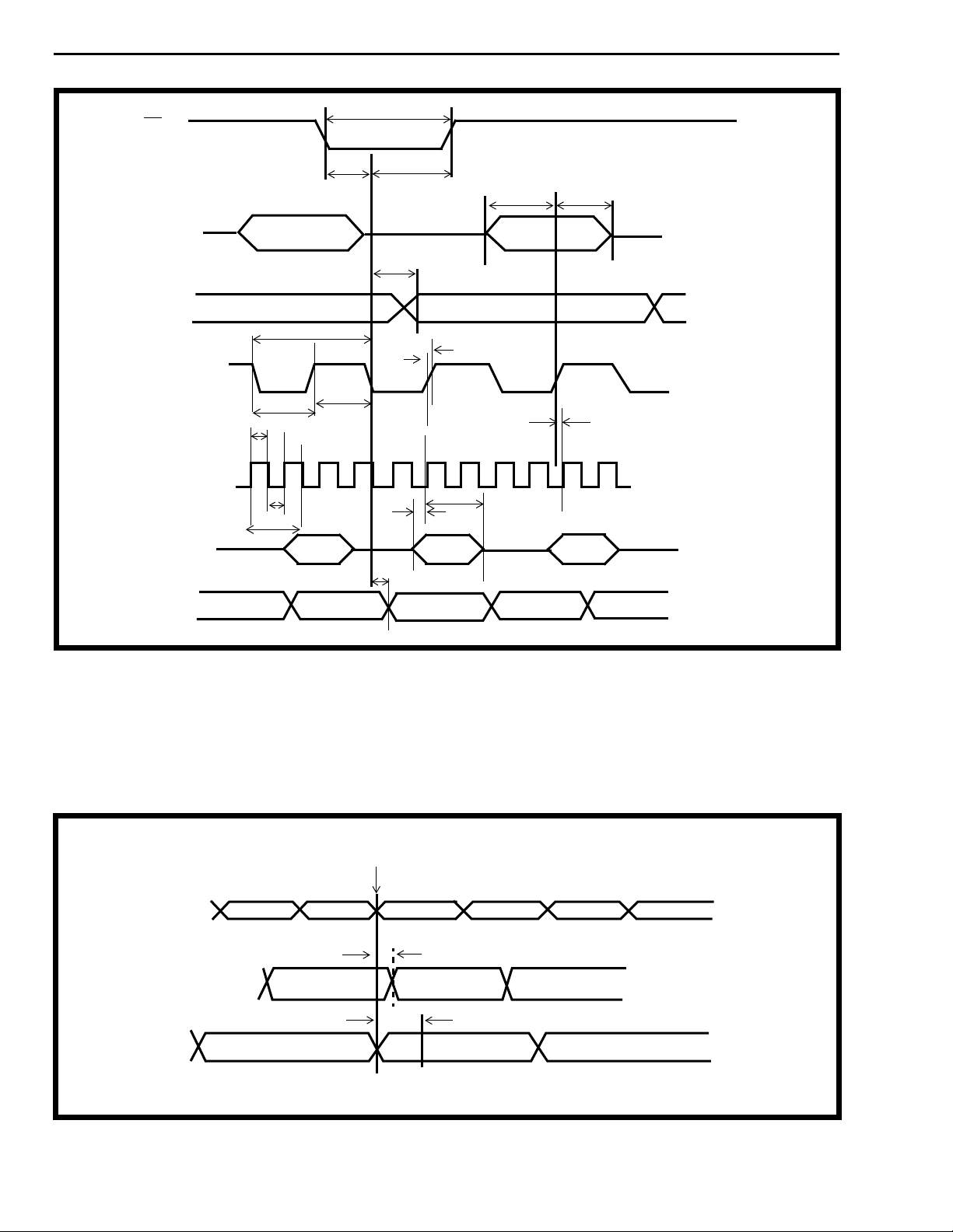
MT90210 Preliminary Information
t
F0i
(8kHz)
hfrw
t
frs
t
frh
t
t
stis
stih
S0-15
(2.048 Mb/s)
(inputs)
S0-15
(2.048 Mb/s)
(outputs)
HC4
(4.096 MHz)
(16.384 MHz)
S16-S23
(8.192 Mb/s)
(inputs)
S16-S23
(8.192 Mb/s)
(outputs)
bit 0, ch. 31
t
clkl
t
bit 1, ch. 127
Figure 19 - Serial Port Timing for Modes 4 and 5
bit 0, ch. 31 bit 7, ch. 0
t
stod
bit 7, ch. 0
t
t
clk
t
hclkl
clkh
hclk
t
hclkh
bit 7,
ch.127
bit 0, ch. 127
t
stod
t
stis
bit 7, ch. 0
t
T
t
stih
bit 0, ch0
bit 1,
bit 1, ch. 0
t
ch
ch.0
2-164
SCLK,
C16+
S0-23
S0-23
bit cell boundary
t
za
t
az
Figure 20 - Serial Port Tri-state Timing
Page 21

Preliminary Information MT90210
AC Electrical Characteristics
†
Characteristics Sym Min Typ* Max Units Test Conditions
1 SCLK, C16 Period
2.048 Mb/s (4.096 MHz)
4.096 Mb/s (8.192 MHz)
8.192 Mb/s (16.384 MHz)
2 SCLK, C16 Pulse Width High
2.048 Mb/s
4.096 Mb/s
8.192 Mb/s
3 SCLK, C16 Pulse Width Low
2.048 Mb/s
4.096 Mb/s
8.192 Mb/s
4 SCLK rise/fall time t
5 HC4 hold related to C16 t
6 HC4 period t
7 HC4 pulse low t
8 HC4 pulse high t
9 Frame Pulse Setup (ST-BUS) t
10 Frame Pulse Hold (ST-BUS) t
11 Frame pulse width in modes 1,2,3
2.048 Mb/s
4.096 Mb/s
8.192 Mb/s
t
clk
t
clkh
t
clkl
T
ch
hclk
hclkl
hclkh
frs
frh
t
frw
244
122
60
122
60
30
122
60
30
ns
ns
ns
ns
ns
ns
ns
ns
ns
5ns
3ns
244 ns
122 ns
122 ns
0ns
10 ns
244
122
60
ns
ns
ns
12 Frame pulse width in modes 4,5 t
13 S0-23 delay from active to High-Z
2.048 Mb/s, 4.096 Mb/s, 8.192 Mb/s
14 S0-23 delay from High-Z to active
2.048 Mb/s, 4.096 Mb/s, 8.192 Mb/s
15 S0-23 Delay (high and low)
hfrw
t
stod
t
az
t
za
244 ns
30 ns RL=1K, CL=200pF
30 ns RL=1K, CL=200pF
from CLK falling (ST-BUS mode)
2.048 Mb/s, 4.096 Mb/s, 8.192 Mb/s
16 S0-23 Set-up Time
t
stis
0
30 ns RL=1K, CL=200pF
before CLK rising (ST-BUS mode)
17 S0-23 Hold Time
t
stih
10
from CLK rising (ST-BUS mode)
18 CKout output delay from SCLK t
† DC Electrical Characteristics are over recommended operating conditions unless otherwise stated.
* Typical figures are at 25°C and are for design aid only.
dpll
5ns
ns
ns
2-165
Page 22
MT90210 Preliminary Information
CKout
(mode 3/4/5)
SCLK
C16+
C16 -
t
dpll
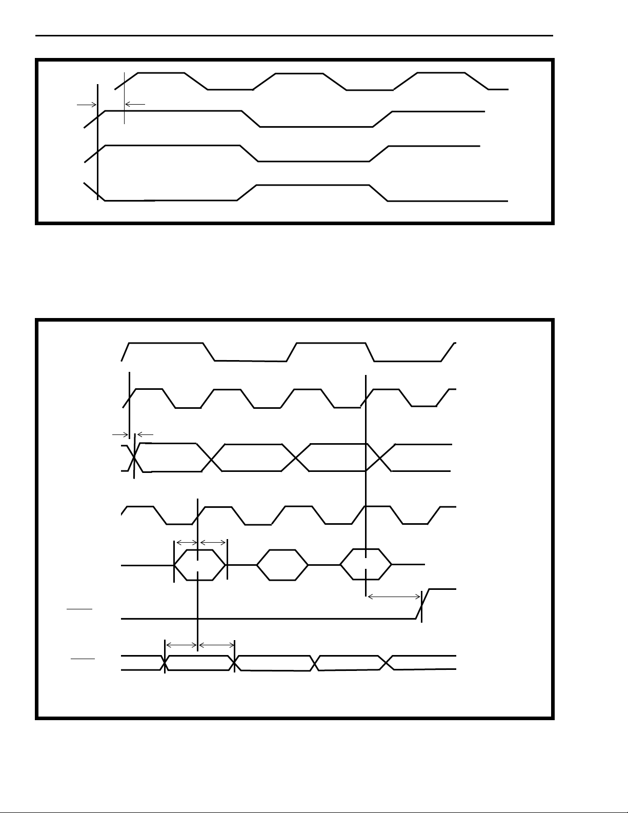
Figure 21 - PLL Timing
SCLK
or
C16+, C16-
CKout
(16.384 MHz,
mode 1)
(32.768 MHz,
mode 2/3/4/5)
A0-A12
RDin
input
P0-P7
(Read/
Write)
Strobe
t
ad
X
t
oes
t
st
X(rd)
t
t
oeh
hd
Y
Y(rd)
Z
Z(rd)
t
stb
OEser
input
Note: R/W1 output signal is HIGH and R/W2 output signal is LOW during read cycles.
Valid
Figure 22 - Parallel Port Data Read Cycle
2-166
Valid
Page 23
Preliminary Information MT90210
SCLK
or
C16+, C16 -
CKout
(16.384 MHz,
mode 1)
(32.768 MHz,
mode 2/3/4/5)
t
ad
A0-A12
t
r/wd
R/W1
t
dod
P0-P7
(Read/
Write)
t
stb
Strobe
Note: R/W2 output signal is HIGH during write cycles.
WR(x)
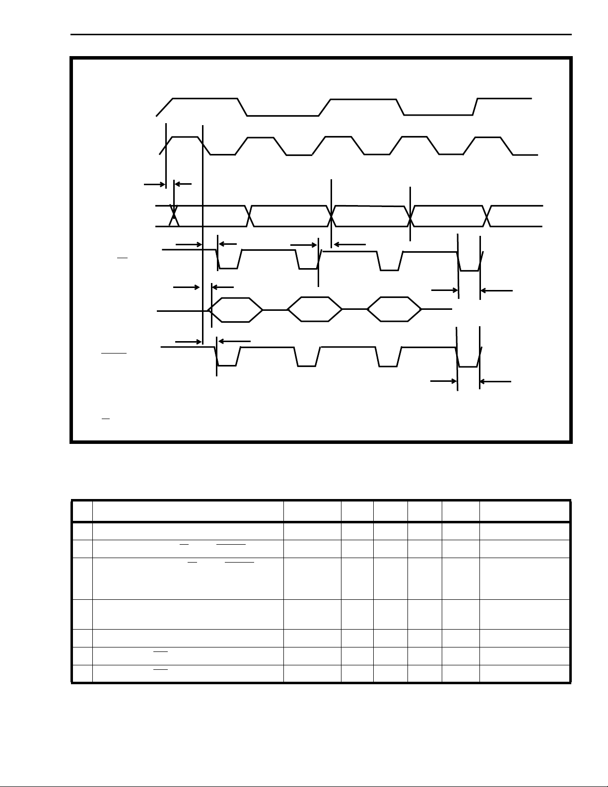
Figure 23- Parallel Port Data Write Cycle
AC Electrical Characteristics
†
YZXS
t
ah
t
pwe
WR(y)
WR(z)
t
pwe
Characteristics Sym Min Typ* Max Units Test Conditions
1 Address Output Delay from Clock t
2 Output Delay on R/W1 and Strobe t
3 Pulse Width Low - R/W1 and Strobe
modes 2, 3, 4 & 5
mode 1
4 Internal Data Output Delay from Clock
ad
r/wd,tstb
t
pwe
t
dod
13.5
30
Falling
5 Address Hold from Write Inactive t
6 Input Data & OE setup times tst, t
7 Input Data & OE hold times thd, t
† DC Electrical Characteristics are over recommended operating conditions unless otherwise stated.
* Typical figures are at 25°C and are for design aid only.
ah
oes
oeh
2.25 ns
0ns
5ns
15 ns output load 50pF
9.5 ns
ns pulse width low on
PCLK for 30 ns
10 ns output load 50 pF
2-167
Page 24

MT90210 Preliminary Information
2-168
Page 25
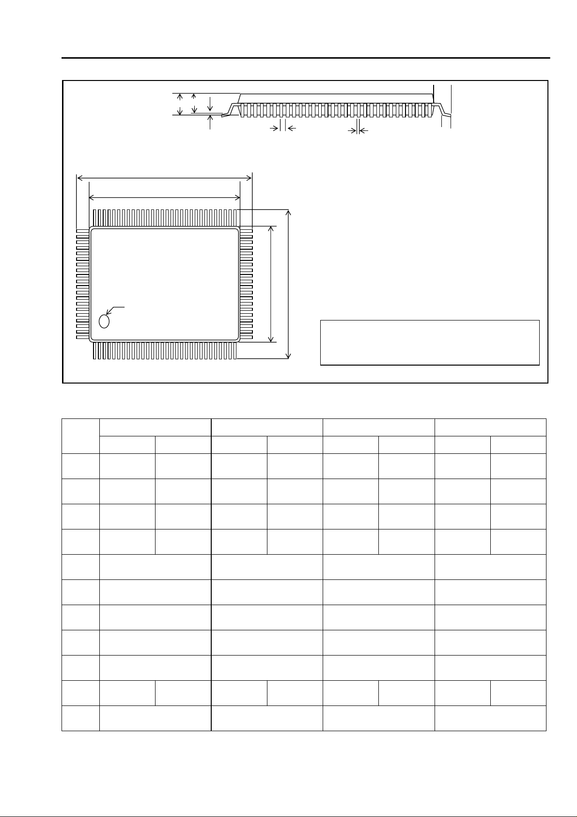
Package Outlines
L1
A
A
2
Pin 1
Index
A
1
D
D
1
e
E
E
1
b
WARNING:
This package diagram does not apply to the MT90810AK
100 Pin Package. Please refer to the data sheet for
exact dimensions.
L
Notes:
1) Not to scale
2) Top dimensions in inches
3) The governing controlling
dimensions are in millimeters
for design purposes ( )
Metric Quad Flat Pack - L Suffix
Dim
Min Max Min Max Min Max Min Max
A - 0.096
(2.45)
A1 0.01
(0.25)
44-Pin 64-Pin 100-Pin 128-Pin
A2 0.077
(1.95)
b 0.01
(0.30)
D 0.547 BSC
(13.90 BSC)
D
1
E 0.547 BSC
E
1
e 0.031 BSC
L 0.029
L1 0.077 REF
0.394 BSC
(10.00 BSC)
(13.90 BSC)
0.394 BSC
(10.00 BSC)
(0.80 BSC)
(0.73)
(1.95 REF)
0.083
(2.10)
0.018
(0.45)
(1.03)
- 0.01
0.04
- 0.134
(0.25)
0.1
(2.55)
0.013
(0.35)
0.941 BSC
(23.90 BSC)
0.787 BSC
(20.00 BSC)
0.705 BSC
(17.90 BSC)
0.551 BSC
(14.00 BSC)
0.039 BSC
(1.0 BSC)
0.029
(0.73)
0.077 REF
(1.95 REF)
(3.40)
- 0.01
0.12
(3.05)
0.02
(0.50)
0.04
(1.03)
- 0.134
(0.25)
0.1
(2.55)
0.009
(0.22)
0.941 BSC
(23.90 BSC)
0.787 BSC
(20.00 BSC)
0.705 BSC
(17.90 BSC)
0.551 BSC
(14.00 BSC)
0.256 BSC
(0.65 BSC)
0.029
(0.73)
0.077 REF
(1.95 REF)
- 0.154
(3.40)
- 0.00 0.01
0.12
(3.05)
0.015
(0.38)
0.04
(1.03)
0.125
(3.17)
0.019
(0.30)
1.23 BSC
(31.2 BSC)
1.102 BSC
(28.00 BSC)
1.23 BSC
(31.2 BSC)
1.102 BSC
(28.00 BSC)
0.031 BSC
(0.80 BSC)
0.029
(0.73)
0.063 REF
(1.60 REF)
(3.85)
(0.25)
0.144
(3.60)
0.018
(0.45)
0.04
(1.03)
NOTE: Governing controlling dimensions in parenthesis ( ) are in millimeters.
Page 26

Package Outlines
Dim
Min Max Min Max Min Max
A - 0.154
(3.92)
A1 0.01
(0.25)
160-Pin 208-Pin 240-Pin
A2 0.125
(3.17)
b 0.009
(0.22)
D 1.23 BSC
(31.2 BSC)
D
1
E 1.23 BSC
E
1
e 0.025 BSC
L 0.029
L1 0.063 REF
1.102 BSC
(28.00 BSC)
(31.2 BSC)
1.102 BSC
(28.00 BSC)
(0.65 BSC)
(0.73)
(1.60 REF)
0.144
(3.67)
0.015
(0.38)
(1.03)
0.04
0.01
(0.25)
.126
(3.20)
.007
(0.17)
0.018
(0.45)
1.204
(30.6)
1.102
(28.00)
1.204 BSC
(30.6 BSC)
1.102 BSC
(28.00 BSC)
0.020 BSC
(0.50 BSC)
0.051 REF
(1.30 REF)
.161
(4.10)
0.02
(0.50)
.142
(3.60)
.011
(0.27)
0.029
(0.75)
- 0.161
0.01
(0.25)
0.126
(3.2)
0.007
(0.17)
1.360 BSC
(34.6 BSC)
1.26 BSC
(32.00 BSC)
1.360 BSC
(34.6 BSC)
1.26 BSC
(32.00 BSC)
0.0197 BSC
(0.50 BSC)
0.018
(0.45)
0.051 REF
(1.30 REF)
(4.10)
0.02
(0.50)
0.142
(3.60)
0.010
(0.27)
0.029
(0.75)
NOTE: Governing controlling dimensions in parenthesis ( ) are in millimeters.
Page 27

http://www.mitelsemi.com
World Headquarters - Canada
Tel: +1 (613) 592 2122
Fax: +1 (613) 592 6909
North America Asia/Pacific Europe, Middle East,
Tel: +1 (770) 486 0194 Tel: +65 333 6193 and Africa (EMEA)
Fax: +1 (770) 631 8213 Fax: +65 333 6192 Tel: +44 (0) 1793 518528
Fax: +44 (0) 1793 518581
Information relating to products and services furnished herein by Mitel Corporation or its subsidiaries (collectively “Mitel”) is believed to be reliable. However, Mitel assumes no
liability for errors that may appear in this publication, or for liability otherwise arising from the application or use of any such information, product or service or for any infringement of
patents or other intellectual property rights owned by third parties which may result from such application or use. Neither the supply of such information or purchase of product or
service conveys any license, either express or implied, under patents or other intellectual property rights owned by Mitel or licensed from third parties by Mitel, whatsoever.
Purchasers of products are also hereby notified that the use of product in certain ways or in combination with Mitel, or non-Mitel furnished goods or services may infringe patents or
other intellectual property rights owned by Mitel.
This publication is issued to provide information only and (unless agreed by Mitel in writing) may not be used, applied or reproduced for any purpose nor form part of any order or
contract nor to be regarded as a representation relating to the products or services concerned. The products, their specifications, services and other information appearing in this
publication are subject to change by Mitel without notice. No warranty or guarantee express or implied is made regarding the capability, performance or suitability of any product or
service. Information concerning possible methods of use is provided as a guide only and does not constitute any guarantee that such methods of use will be satisfactory in a specific
piece of equipment. It is the user’s responsibility to fully determine the performance and suitability of any equipment using such information and to ensure that any publication or
data used is up to date and has not been superseded. Manufacturing does not necessarily include testing of all functions or parameters. These products are not suitable for use in
any medical products whose failure to perform may result in significant injury or death to the user. All products and materials are sold and services provided subject to Mitel’s
conditions of sale which are available on request.
M Mitel (design) and ST-BUS are registered trademarks of MITEL Corporation
Mitel Semiconductor is an ISO 9001 Registered Company
Copyright 1999 MITEL Corporation
All Rights Reserved
Printed in CANADA
TECHNICAL DOCUMENTATION - NOT FOR RESALE
 Loading...