

Page 1
CMOS ST-BUS FAMILY
Enhanced Digital Switch
Advance Information
MT89L85
Features
• 3.3 volt supply
• 5V tolerant inputs and TTL compatible outputs
• 256 x 256 channel non-blocking switch
• Programmable frame integrity for wideband
channels
• Automatic identification of ST-BUS/GCI
interface backplanes
• Per channel tristate control
• Patented message mode
• Non-multiplexed microprocessor interface
• Available in PLCC-44 and SSOP-48 packages
• Pin compatible with MT8985 device
• Low power consumption
Applications
• Medium size digital switch matrices
• Hyperchannel switching (e.g., ISDN H0)
• ST-BUS/MVIP™ interface functions
• Serial bus control and monitoring
• Centralized voice processing systems
• Data multiplexer
DS5194 ISSUE 2 September 1999
Ordering Information
MT89L85AP 44 Pin PLCC
MT89L85AN 48 Pin SSOP
-40°C to +85°C
Description
The MT89L85 Enhanced Digital Switch device is an
upgraded 3-volt version of the MT8985 Digital
Switch. It is pin compatible with the MT8985 and
retains all of the MT8985's functionality. The
enhanced digital swtich is designed for switching
PCM-encoded voice or data, under microprocessor
control, in digital exchanges, PBXs and any ST-BUS/
MVIP environment. It provides simultaneous
connections for up to 256 64kb/s channels. Each of
the eight serial inputs and outputs consist of 32 64
kbit/s channels multiplexed to form a 2048 kbit/s
stream. As the main function in switching
applications, the device provides per-channel
selection between variable or constant throughput
delays. The constant throughput delay feature allows
grouped channels such as ISDN H0 to be switched
through the device maintaining its sequence
integrity. The MT89L85 is ideal for medium sized
mixed voice/data switch and voice processing
applications.
STi0
STi1
STi2
STi3
STi4
STi5
STi6
STi7
** for 48-pin SSOP only
Serial
to
Parallel
Converter
**
V
DD
Data
Memory
F0i
C4i
Frame
Counter
DS
RESET
Control Register
Control Interface
CS R/W A5/A0DTA D7/
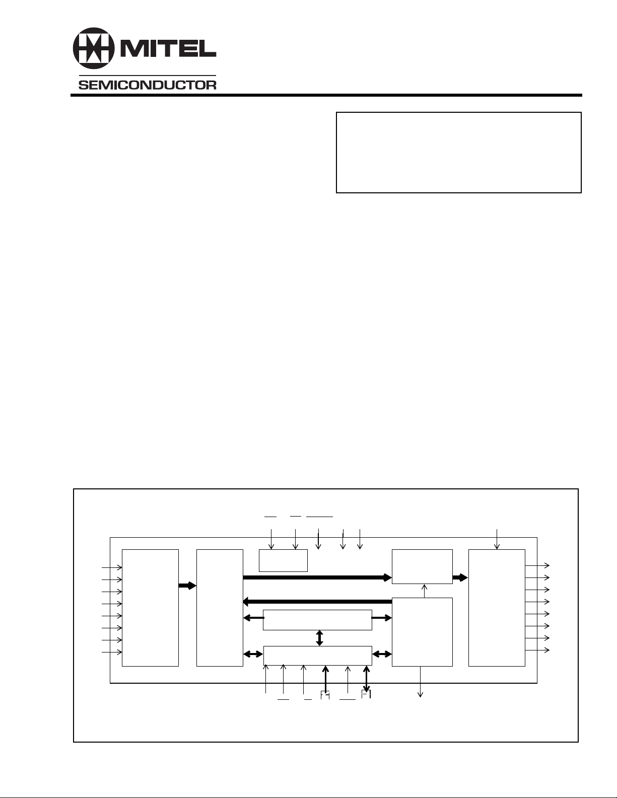
Figure 1 - Functional Block Diagram
V
SS
Output
MUX
Connection
Memory
D0
CSTo
ODE
Parallel
to
Serial
Converter
STo0
STo1
STo2
STo3
STo4
STo5
STo6
STo7
1
Page 2
MT89L85 Advance Information
STi3
STi4
STi5
STi6
STi7
V
DD
F0i
C4i
A0
A1
A2
NC
STi1
STi2
STi0
65432
7
8
9
10
11
12
13
14
15
16
17
1819202122
A4
A3
NC
A5
44 PIN PLCC
DTA
ODE
CSTo
1
4443424140
23
2425262728
W
CS
DS
R/
STo1
D6
NC
STo2
39
38
37
36
35
34
33
32
31
30
29
D5
NC
STo3
STo4
STo5
STo6
STo7
V
SS
D0
D1
D2
D3
D4
STo0
D7
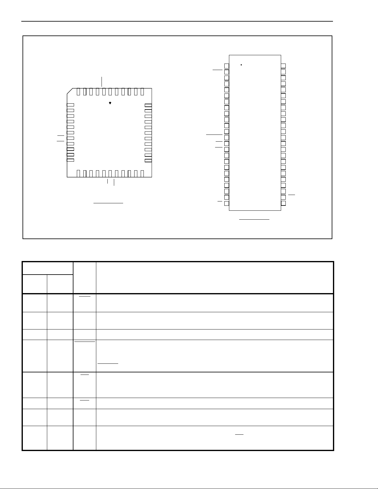
Figure 2 - Pin Connections
V
DTA
STi0
STi1
STi2
NC
STi3
STi4
STi5
STi6
STi7
V
RESET
C4i
NC
DS
R/W
1
SS
2
3
4
5
6
7
8
9
10
11
12
DD
13
14
F0i
15
16
A0
17
A1
18
A2
19
20
A3
21
A4
22
A5
23
24
48 PIN SSOP
(JEDEC MO-118, 300mil Wide)
48
47
46
45
44
43
42
41
40
39
38
37
36
35
34
33
32
31
30
29
28
27
26
25
CSTo
ODE
STo0
STo1
STo2
NC
STo3
STo4
STo5
STo6
STo7
V
SS
V
DD
D0
D1
D2
D3
D4
NC
D5
D6
D7
CS
V
SS
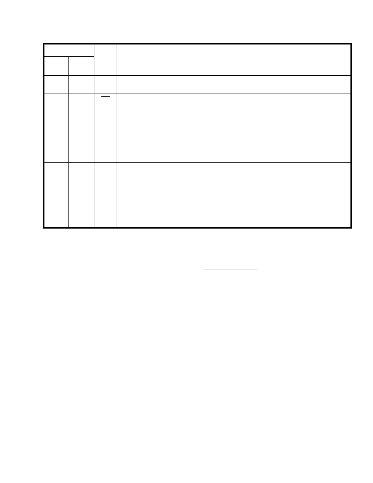
Pin Description
Pin #
44
PLCC48SSOP
22DTA Data Acknowledgment (Open Drain Output). This active low output indicates that a
3-5
7-11
3-5
7-11
12 12,36 V
13 RESET Device Reset (5v-tolerant input). This pin is only available for the 48-pin SSOP
13 14 F0i Frame Pulse (Input). This input accepts and automatically identifies frame
14 15 C4i Clock (Input). 4.096 MHz serial clock for shifting data in and out of the data streams.
15-17
19-21
16-18
20-22
22 23 DS Data Strobe (Input). This is the input for the active high data strobe on the
Name Description
data bus transfer is complete. A pull-up resistor is required at this output.
STi0-
STi7
ST-BUS Input 0 to 7 (Inputs). Serial data input streams. These streams have 32
channels at data rates of 2.048 Mbit/s.
+3.3 Volt Power Supply.
DD
package. This active lo w input puts the MT89L85 in its reset state. It clears the internal
counters anf registers. All ST-BUS outputs are set to the high impedance state. This
RESET pin must be held low for a minimum of 100nsec to reset the device.
synchronization signals formatted according to different backplane specifications such
as ST-BUS and GCI.
A0-A5 Address 0 to 5 (Inputs). These lines provide the address to MT89L85 internal
registers.
microprocessor interface. This input operates with CS to enable the internal read and
write generation.
2
Page 3
Advance Information MT89L85
Pin Description
Pin #
44
PLCC48SSOP
23 24 R/W Read/Write (Input). This input controls the direction of the data bus lines (D0-D7)
24 26 CS Chip Select (Input). Active low input enabling a microprocessor read or write of
25-27
29-33
34 1,25,37 V
35-39
41-43
44 47 ODE Output Drive Enable (Input). This is an output enable for the STo0 to STo7 serial
1 48 CSTo Control ST-BUS Output (Output). This output is a 2.048 Mb/s line which contains 256
6,18,
28,40
27-29
31-35
38-42
44-46
6,19,30,43NC No Connection.
Name Description
during a microprocessor access.
control register or internal memories.
D7-D0 Data Bus 7 to 0 (Bidirectional). These pins provide microprocessor access to data in
the internal control register, connect memory high, connect memory low and data
memory.
Ground Rail.
SS
STo7-
STo0
ST-BUS Outputs 7 to 0 (Three-state Outputs). Serial data output streams. These
streams are composed of 32 channels at data rates of 2.048 Mbit/s.
outputs. If this input is low STo0-7 are high impedance. If this input is high each
channel may still be put into high impedance by software control.
bits per frame. The level of each bit is controlled by the contents of the CSTo bit in the
Connect Memory high locations.
Functional Description
With the integration of voice, video and data services
into the same network, there has been an increasing
demand for systems which ensure that data at N x 64
Kbit/s rates maintain frame sequence integrity while
being transported through time slot interchange
circuits. Existing requirements demand time slot
interchange devices performing switching with
constant throughput delay while guaranteeing
minimum delay for voice channels.
The MT89L85 device provides both functions and
allows existing systems based on the MT8985 to be
easily upgraded to maintain the data integrity while
multiple channel data are transported. The device is
designed to switch 64 kbit/s PCM or N x 64 kbit/s
data. The MT89L85 can provide both frame integrity
for data applications and minimum throughput
switching delay for voice applications on a per
channel basis.
By using Mitel Message mode capability, the
microprocessor can access input and output time
slots on a per channel basis to control devices such
as the MITEL MT8972, ISDN Transceivers and T1/
CEPT trunk interfaces through the ST-BUS interface.
Different digital backplanes can be accepted by the
MT89L85 device without user's intervention. The
MT89L85 device provides an internal circuit that
automatically identifies the polarity and format of
frame synchronization input signals compatible to
ST-BUS and GCI interfaces.
Device Operation
A functional block diagram of the MT89L85 device is
shown in Figure 1. The serial ST-BUS streams
operate continuously at 2.048 Mb/s and are arranged
in 125 µs wide frames each containing 32 8-bit
channels. Eight input (STi0-7) and eight output
(STo0-7) serial streams are provided in the MT89L85
device allowing a complete 256 x 256 channel nonblocking switch matrix to be constructed. The serial
interface clock for the device is 4.096 MHz, as
required in ST-BUS and GCI specifications.
Data Memory
The received serial data is converted to parallel
format by the on-chip serial to parallel converters
and stored sequentially in a 256-position Data
Memory. The sequential addressing of the Data
Memory is generated by an internal counter that is
reset by the input 8 kHz frame pulse (F0i) marking
the frame boundaries of the incoming serial data
streams.
Depending on the type of information to be switched,
the MT89L85 device can be programmed to perform
3
Page 4

MT89L85 Advance Information
time slot interchange functions with different
throughput delay capabilities on a per-channel basis.
For voice applications, the variable delay mode can
be selected ensuring minimum throughput delay
between input and output data. In multiple or
grouped channel data applications, the constant
delay mode can be selected maintaining the integrity
of the information through the switch.
Data to be output on the serial streams may come
from two sources: Data Memory or Connect Memory.
Locations in the Connect Memory, which is split into
HIGH and LOW parts, are associated with particular
ST-BUS output streams. When a channel is due to
be transmitted on an ST-BUS output, the data for the
channel can either be switched from an ST-BUS
input (connection mode) or it can be originated from
the microprocessor (message mode). If a channel is
configured in connection mode, the source of the
output data is the Data Memory. If a channel is
configured in message mode, the source of the
output data is the Connect Memory Low. Data
destined for a particular channel on the serial output
stream is read from the Data or Connect Memory
Low during the previous channel time slot. This
allows enough time for memory access and internal
parallel to serial conversion.
three-state condition. In addition, the Connect
Memory High provides one bit to allow the user to
control the state of the CSTo output pin.
If an output channel is set to three-state condition,
the TDM serial stream output will be placed in high
impedance during that channel time. In addition to
the per-channel three-state control, all channels on
the TDM outputs can be placed in high impedance at
one time by pulling the ODE input pin in LOW. This
overrides the individual per-channel programming on
the Connect Memory High bits.
The Connect Memory data is received via the
Microprocessor Interface at D0-D7 lines. The
addressing of the MT89L85 internal registers, Data
and Connect memories is performed through
address input pins and some bits of the device's
Control register. The higher order address bits come
from the Control register, which may be written or
read through the microprocessor interface. The low er
order address bits come directly from the external
address line inputs. For details on the device
addressing, see Software Control and Control
register description.
Serial Interface Timing
Connection and Message Modes
In connection mode, the addresses of input source
for all output channels are stored in the Connect
memory Low. The Connect Memory Low locations
are mapped to each location corresponding to an
output 64 kb/s channel. The contents of the Data
memory at the selected address are then transferred
to the parallel to serial converters. By having the
output channel to specify the input channel through
the connect memory, the user can route the same
input channel to several output channels, allowing
broadcasting facility in the switch.
In message mode the CPU writes data to the
Connect Memory Low locations which correspond to
the output link and channel number. The contents of
the Connect Memory Low are transferred to the
parallel to serial converter one channel before it is to
be output. The Connect Memory Low data is
transmitted each frame to the output until it is
changed by the CPU.
The per-channel functions available in the MT89L85
are controlled by the Connect Memory High bits,
which determine whether individual output channels
are selected into specific conditions such as:
message or connection mode, variable or constant
throughput delay modes, output drivers enabled or in
The MT89L85 master clock (
allowing serial data link configuration at 2.048 Mb/s
to be implemented. The MT89L85 frame
synchronization pulse can be formatted according to
ST-BUS or GCI interface specifications; i.e., the
frame pulse can be active in HIGH (GCI) or LOW
(ST-BUS). The MT89L85 device automatically
detects the presence of an input frame pulse and
identifies the type of backplane present on the serial
interface. Upon determining the correct interface
connected to the serial port, the inter nal timing unit
establishes the appropriate serial data bit transmit
and sampling edges. In ST-BUS mode, every second
falling edge of the 4.096 MHz clock marks a bit
boundary and the input data is clocked in by the
rising edge, three quarters of the way into the bit cell.
In GCI mode, every second rising edge of the 4.096
MHz clock marks the bit boundary while data
sampling is performed during the falling edge, at
three quarters of the bit boundaries.
Delay through the MT89L85
The transfer of information from the input serial
streams to the output serial streams results in a
delay through the MT89L85 device. The delay
through the device varies according to the mode
selected in the V/C bit of the connect memory high.
C4i) is a 4.096 MHz
2-4
Page 5
Advance Information MT89L85
Variable Delay mode
The delay in this mode is dependent only on the
combination of source and destination channels and
it is not dependent on the input and output streams.
The minimum delay achievable in the MT89L85
device is 3 time slots. In the MT89L85 device, the
information that is to be output in the same channel
position as the information is input (position n),
relative to frame pulse, will be output in the following
frame (channel n, frame n+1). The same occurs if
the input channel has to be output in the two
channels succeeding (n+1 and n+2) the channel
position as the information is input.
The information switched to the third timeslot after
the input has entered the device (for instance, input
channel 0 to output channel 3 or input channel 30 to
output channel 1), is always output three channels
later.
Any switching configuration that provides three or
more timeslots between input and output channels,
will have a throughput delay equal to the difference
between the output and input channels; i.e., the
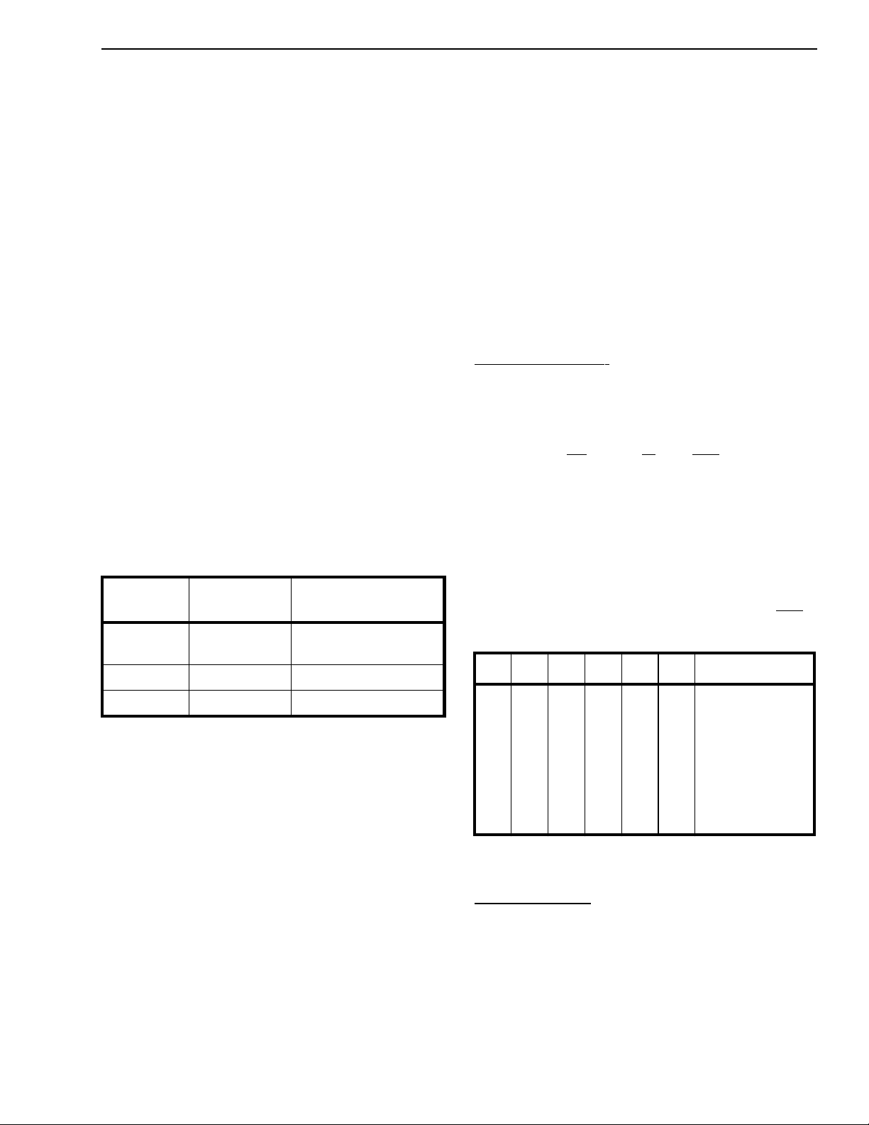
throughput delay will be less than one frame. Table 1
shows the possible delays for the MT89L85 device in
Variable Delay mode:
Input
Channel
n m=n, n+1 or
n m>n+2 m-n time slots
n m<n 32-(n-m) time slots
Table 1 - Channel Delay for the Variable Delay
Constant Delay Mode
In this mode frame integrity is maintained in all
switching configurations by making use of a multiple
Data-Memory buffer technique where input channels
written in any of the buffers during frame N will be
read out during frame N+2. In the MT89L85, the
minimum throughput delay achieve-able in Constant
Delay mode will be 32 time slots; for example, when
input time slot 32 (channel 31) is switched to output
time slot 1 (channel 0). Likewise, the maximum delay
is achieved when the first time slot in a frame
(channel 0) is switched to the last time slot in the
frame (channel 31), resulting in 94 time slots of
delay.
Output
Channel
n+2
Mode
Throughput Delay
m-n + 32 timeslots
To summarize, any input time slot from input frame N
will be always s witched to the destination time slot on
output frame N+2. In Constant Delay mode, the
device throughput delay is calculated according to
the following formula:
DELAY = [32 + (32 - IN) + (OUT - 1)];
(expressed in number of time slots)
Where: IN is the number of the input time slot
(from 1 to 32).
OUT is the number of the output time slot
(from 1 to 32).
Microprocessor Port
The MT89L85 microprocessor port has pin
compatibility with Mitel MT8985 Digital Switch
devices providing a non-multiplexed bus architecture.
The parallel port consists of an 8 bit parallel data bus
(D0-D7), six address input lines (A0-A5) and four
control lines (CS, DS, R/W and DTA). This parallel
microport allows the access to the Control registers,
Connection Memory High, Connection Memory Low
and the Data Memory. All locations are read/written
except for the data memory which can be read only.
Accesses from the microport to the connection
memory and the data memory are multiplexed with
accesses from the input and output TDM ports. This
can cause variable Data Acknowledge delays (DTA).
A5 A4 A3 A2 A1 A0 LOCATION
0
0
0
0
0
0
Control Register
1
0
0
0
0
0
1
0
0
0
0
1
1
•
•
•
•
•
1
•
•
•
•
•
1
•
•
•
•
•
1
•
•
•
•
•
1
•
•
•
•
•
1
1
1
1
1
1
Figure 3 - Address Memory Map
Note: "x" Don’t care
Software Control
The address lines on the microprocessor interface
give access to the MT89L85 internal registers and
memories. If the A5,A1,A0 address line inputs are
LOW, then the MT89L85 Inter nal Control Register is
addressed (see Figure 3). If A5 input line is HIGH,
then the remaining address input lines are used to
select Memory subsections of 32 locations
corresponding to the number of channels per input or
output stream. As explained in the Control register
Channel 0
Channel 1
•
•
•
•
•
Channel 31
2-5
Page 6
MT89L85 Advance Information
description, the address input lines and the Stream
Address bits (STA) of the Control register give the
user the capability of selecting all positions of the
MT89L85 Data and Connect memories.
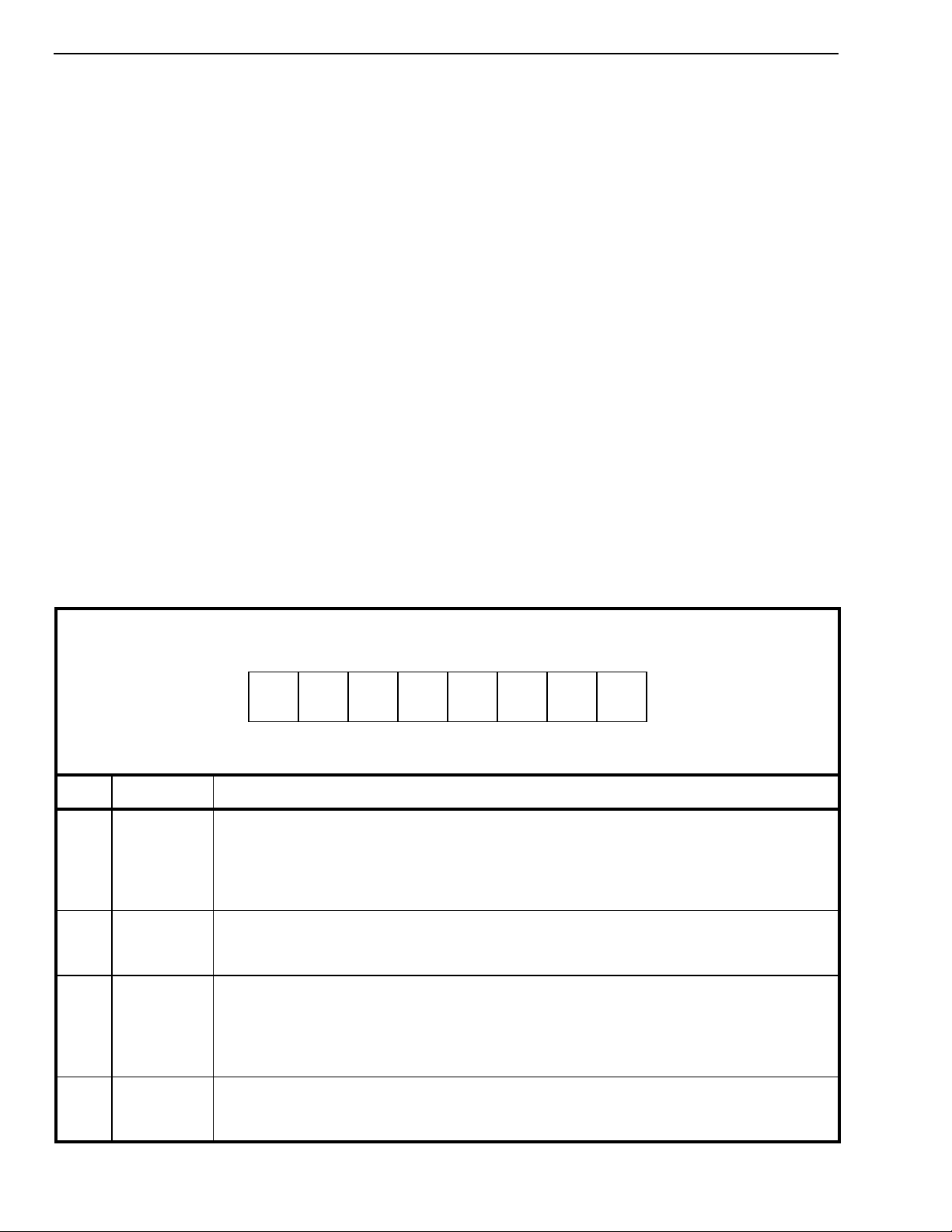
The data in the Control register consists of Split
memory and Message mode bits, Memory select and
Stream Address bits (see Figure 4). The memory
select bits allow the Connect Memory HIGH or LOW
or the Data Memory to be chosen, and the Stream
Address bits define an internal memory subsections
corresponding to input or output ST-BUS streams.
Bit 7 (Split Memory) of the Control register allows
split memory operation whereby reads are from the
Data memory and writes are to the Connect Memor y
LOW.
The Message Enable bit (bit 6) places every output
channel on every output stream in message mode;
i.e., the contents of the Connect Memory LOW
(CML) are output on the ST-BUS output streams
once every frame unless the ODE input pin is LOW.
If ME bit is HIGH, then the MT89L85 behaves as if
bits 2 (Message Channel) and 0 (Output Enable) of
every Connect Memory HIGH (CMH) locations were
set to HIGH, regardless of the actual value. If ME bit
is LOW, then bit 2 and 0 of each Connect Memor y
HIGH location operates normally. In this case, if bit 2
of the CMH is HIGH, the associated ST-BUS output
channel is in Message mode. If bit 2 of the CMH is
LOW, then the contents of the CML define the source
information (stream and channel) of the time slot that
is to be switched to an output.
If the ODE input pin is LOW, then all ser ial outputs
are high-impedance. If ODE is HIGH, then bit 0
(Output Enable) of the CMH location enables (if
HIGH) or disables (if LOW) the output drivers for the
corresponding individual ST-BUS output stream and
channel.
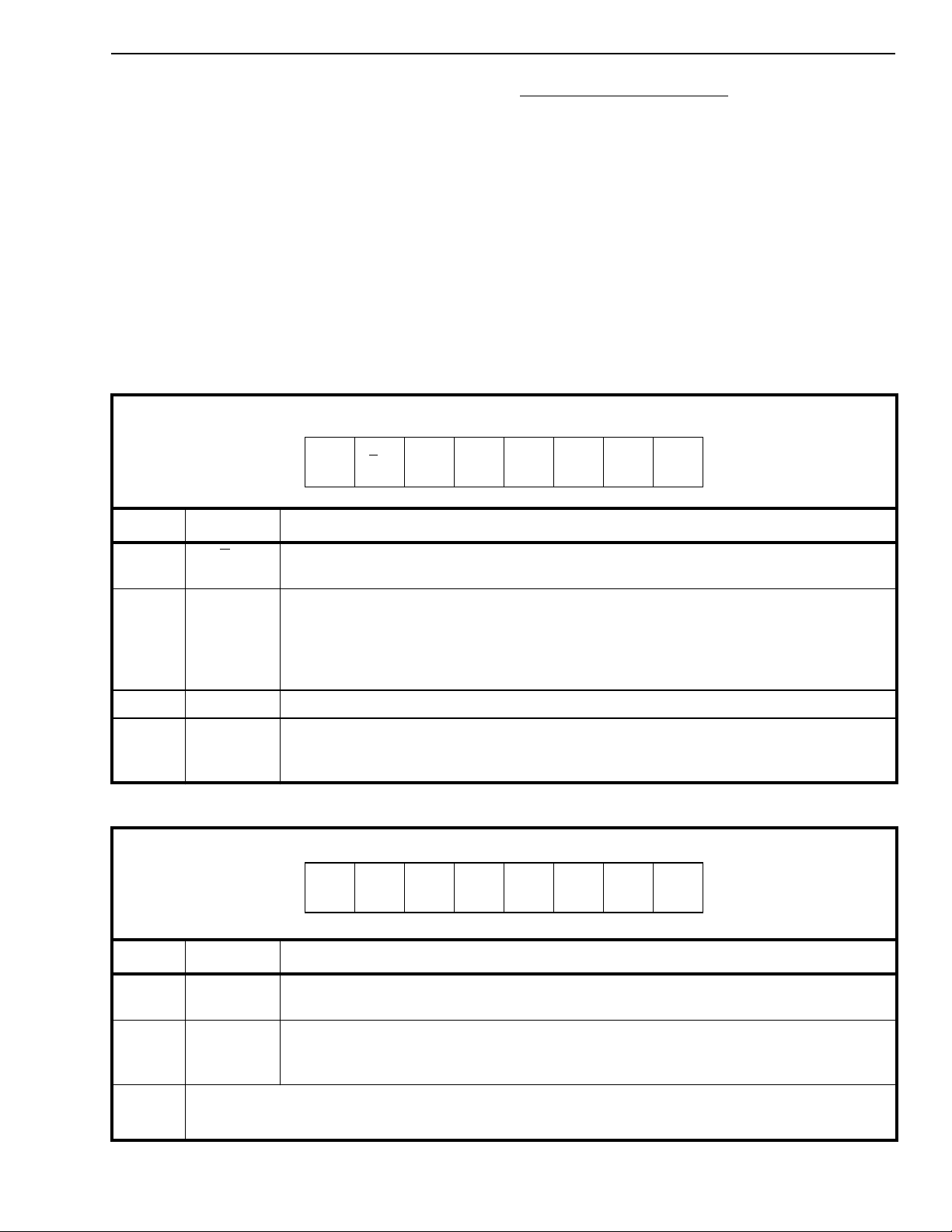
The contents of bit 1 (CSTo) of each Connection
Memory High location (see Figure 5) is output on
CSTo pin once every frame. The CSTo pin is a 2048
Mbit/s output which carries 256 bits. If CSTo bit is set
HIGH, the corresponding bit on CSTo output is
transmitted in HIGH. If CSTo bit is LOW, the
corresponding bit on the CSTo output is transmitted
in LOW. The contents of the 256 CSTo bits of the
CMH are transmitted sequentially on to the CSTo
output pin and are synchronous to the ST-BUS
streams. To allow for delay in any external control
76543210
SM ME X MS1 MS0 STA2 STA1 STA0
BIT NAME DESCRIPTION
7 SM Split Memory. When 1, all subsequent reads are from the Data Memory and writes are to
the Connection Memory Low, except when the Control Register is accessed again. The
Memory Select bits need to be set to specify the memory for the operations. When 0, the
Memory Select bits specify the memory for subsequent operations. In either case, the
Stream Address Bits select the subsection of the memory which is made available.
6 ME Message Enable. When 1, the contents of the Connection Memory Low are output on the
Serial Output streams except when in High Impedance. When 0, the Connection Memory
bits for each channel determine what is output.
4-3 MS1-MS0 Memory Select Bits. The memory select bits operate as follows:
0-0 - Not to be used
0-1 - Data Memory (read only from the CPU)
1-0 - Connection Memory Low
1-1 - Connection Memory High
2-0 ST A2-0 Stream Address Bits 2-0. The number e xpressed in binary notation on these bits refers to
the input or output ST-BUS stream which corresponds to the subsection of memory made
accessible for subsequent operations.
x = Don’t care
Figure 4 - Control Register Bits
6
Page 7
Advance Information MT89L85
circuitry the contents of the CSTo bit is output one
channel before the corresponding channel on the STBUS streams. For example, the contents of CSTo bit
in position 0 (ST0, CH0) of the CMH, is transmitted
synchronously with ST-BUS channel 31, bit 7. The
contents of CSTo bit in position 32 (ST1, CH0) of the
CMH is transmitted during ST-BUS channel 31 bit 6.
Bit V/C (Variable/Constant Delay) on the Connect
Initialization of the MT89L85
On initialization or power up, the contents of the
Connection Memory High can be in any state. This
is a potentially hazardous condition when multiple
MT89L85 ST-BUS outputs are tied together to form
matrices, as these outputs may conflict. The ODE
pin should be held low on power up to keep all
outputs in the high impedance condition.
Memory High locations allow per-channel selection
between Variable and Constant throughput delay
capabilities.
76543210
X V/C X X X MC CSTo OE
BIT NAME DESCRIPTION
6 V/C Variable/Constant Throughput Delay Mode. This bit is used to select between Variable
(LOW) and Constant Delay (HIGH) modes on a per-channel basis.
2 MC Message Channel. When 1, the contents of the corresponding location in Connection
Memory Low are output on the corresponding channel and stream. When 0, the contents
of the programmed location in Connection Memory Low act as an address for the Data
Memory and so determine the source of the connection to the location’s channel and
stream.
1 CSTo CSTo Bit. This bit drives a bit time on the CSTo output pin.
0 OE Output Enable. This bit enables the output drivers on a per-channel basis. This allows
individual channels on individual streams to be made high-impedance, allowing switch
matrices to be constructed. A HIGH enables the driver and a LOW disables it.
Figure 5 - Connection Memory High Bits
x = Don’t care
76543210
SAB2 SAB1 SAB0 CAB4 CAB3 CAB2 CAB1 CAB0
BIT NAME DESCRIPTION
7-5 SAB2-0* Source Stream Address bits. These three bits are used to select eight source streams
for the connection. Bit 7 of each word is the most significant bit.
4-0* CAB4-0* Source Channel Address bits 0-4. These five bits are used to select 32 different source
channels for the connection (The ST-BUS stream where the channel is present is defined
by bits SAB2-0). Bit 4 is the most significant bit.
If bit 2 of the corresponding Connection High location is 1 or if bit 6 of the Control Register is 1, then these entire 8 bits are output
*
on the channel and stream associated with this location. Otherwise, the bits are used as indicated to define the source of the
connection which is output on the channel and stream associated with this location.
Figure 6 - Connection Memory Low Bits
7
Page 8
MT89L85 Advance Information
During the microprocessor initialization routine, the
microprocessor should program the desired active
paths through the matrices, and put all other
channels into the high impedance state. Care should
be taken that no two connected ST-BUS outputs
drive the bus simultaneously. When this process is
complete, the microprocessor controlling the
matrices can bring the ODE signal high to relinquish
high impedance state control to the CMHb0s.
Applications
Typical Exchange, PBX or Multiplexer
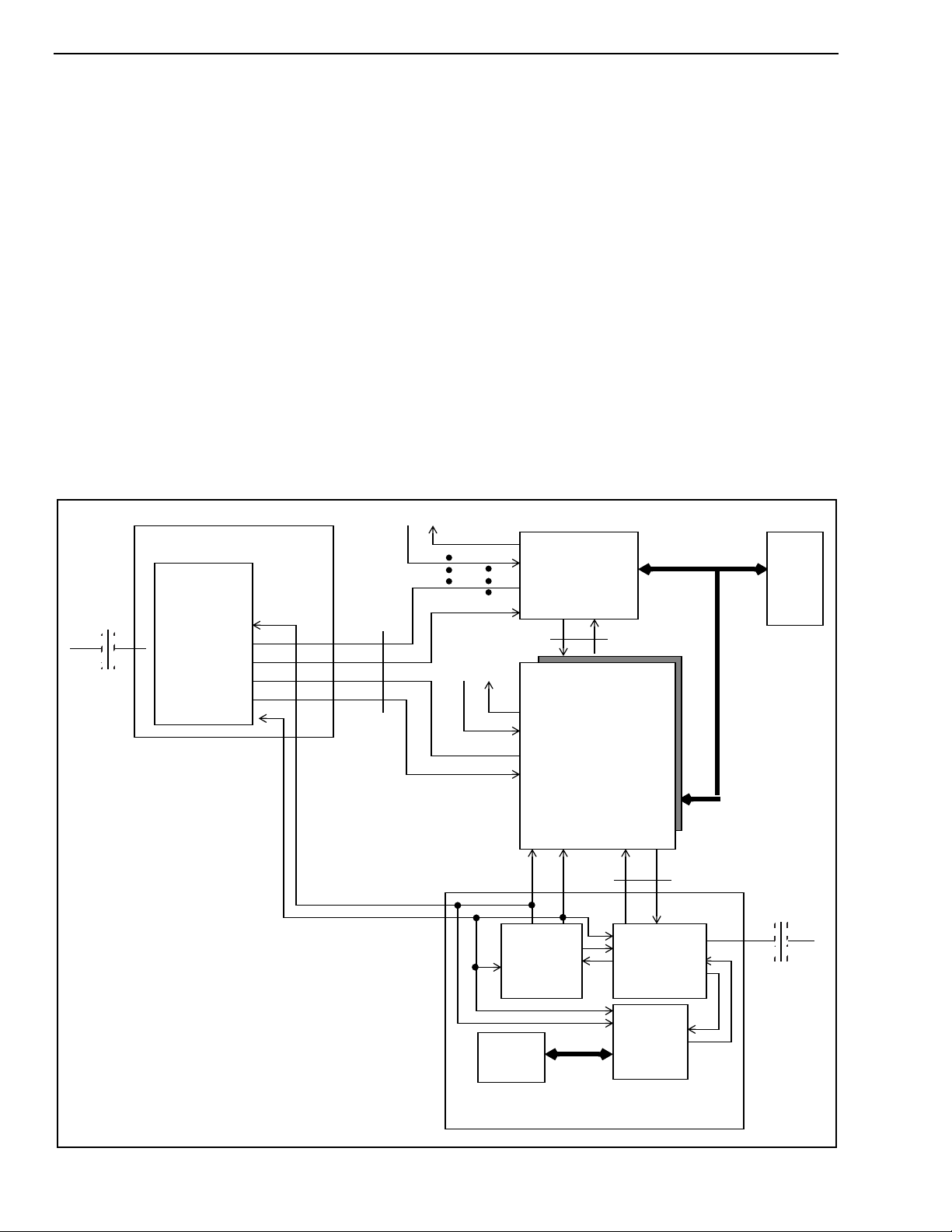
Figure 7 shows a typical implementation of line cards
being interconnected through a central routing matrix
that can scale up in channel capacity to
accommodate different number of ports depending
on the application. In a configuration where the
switched services utilize concatenated or grouped
To other lines
time slots to carry voice, data and video (channels of
128, 256 Kb/s, ISDN H0 and others), the central
routing matrix has to guarantee constant throughput
delay to maintain the sequence integrity between
input and output channels. Figure 7 shows an
example where the MT89L85 device guarantees
data integrity when data flows from the T1/E1 to the
S/U interface links and vice-versa. Modern
technologies available today such as Frame Relay
network using dedicated fractional T1 are one of the
key applications for the MT89L85 device.
Low Latency Isochronous Network
In today's local working group environment, there is
an increasing demand for solutions on
interconnection of desktop and telephone systems
so that mixed voice, data and video services can be
grouped together in a reliable network allowing the
deployment of multimedia services. Existing
multimedia applications require a network with
S/U
Basic Rate Line Card
MT8930/31
MT8910
MT8972
ST-BUS
To other lines
MT8940/
MT8941
Layers
2 & 3
Entity
ST-BUS
ROUTING
MATRIX
MT89L85’s
MH89760/
MH89790
ST-BUS
T1/E1
Link
C
P
U
MT8920
µC
Primary Rate Card
Figure 7 - Typical Exchange, PBX or Multiplexer Configuration
8
Page 9
Advance Information MT89L85
ISDN Desktops
(2B+D)
• • • • • •
Analog Connections
• • • • • •
Server 2
T1
Access to
Public
Network
T1/E1
Server 3
Isochronous Network
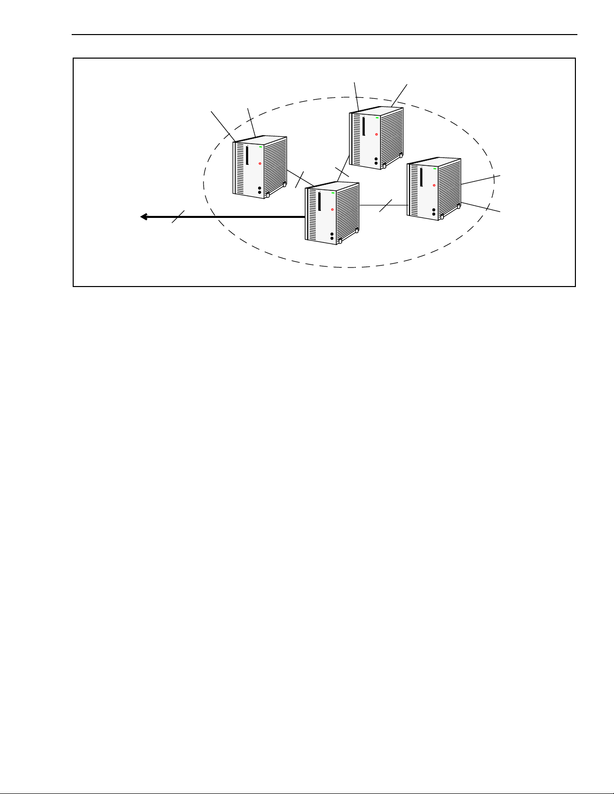
Figure 8a - Private Isochronous Network
predictable data transfer delays that can be
implemented at a reasonable cost. The Low Latency
Isochronous Network is one of the alternatives that
system designers have chosen to accommodate this
requirement (see Figure 8a). This network can be
implemented using existing TDM transmission media
devices such as ISDN Basic (S or U) and Primary
rates trunks (T1 and CEPT) to transport mixed voice
and data signals in grouped time slots; for example,
2B channels in case of ISDN S or U interfaces or up
to 32 channels in case of a CEPT link.
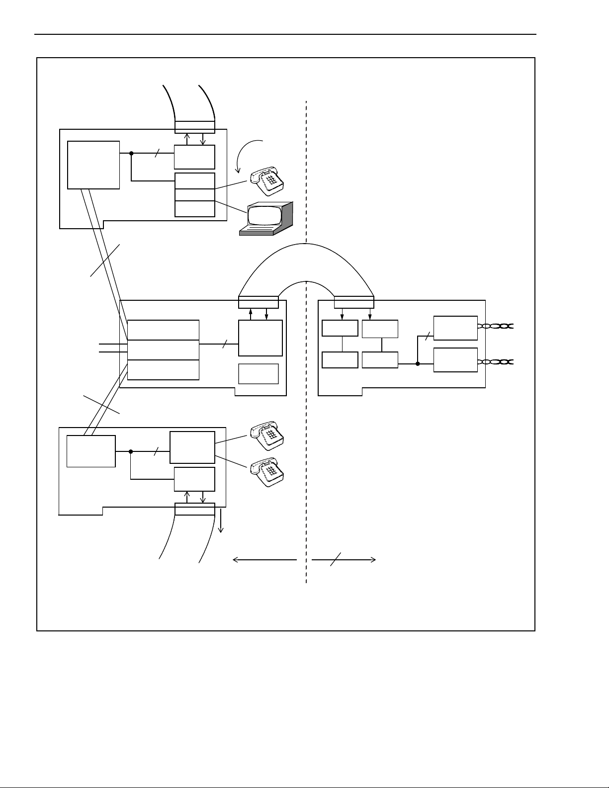
Figure 8b shows a more detailed configuration
whereby several PCs are connected to form an
Isochronous network. Several services can be
interconnected within a single PC chassis through
the standardized Multi Vendor Integration Protocol
(MVIP). Such an interface allows the distribution and
interconnection of services like voice mail, integrated
voice response, voice recognition, LAN gateways,
key systems, fax servers, video cards, etc.
Server 1
T1
E1
Server 4
n x 64
Connections
(e.g. Video)
• • • • • •
The information being exchanged between cards
through the MVIP interface on every computer as
well as between computers through T1 or CEPT links
is, in general, of mixed type where 64Kb/s and
N*64Kb/s channels are grouped together. When
such a mixed type of data is transferred between
cards within one chassis or from one computer to
another, the sequence integrity of the concatenated
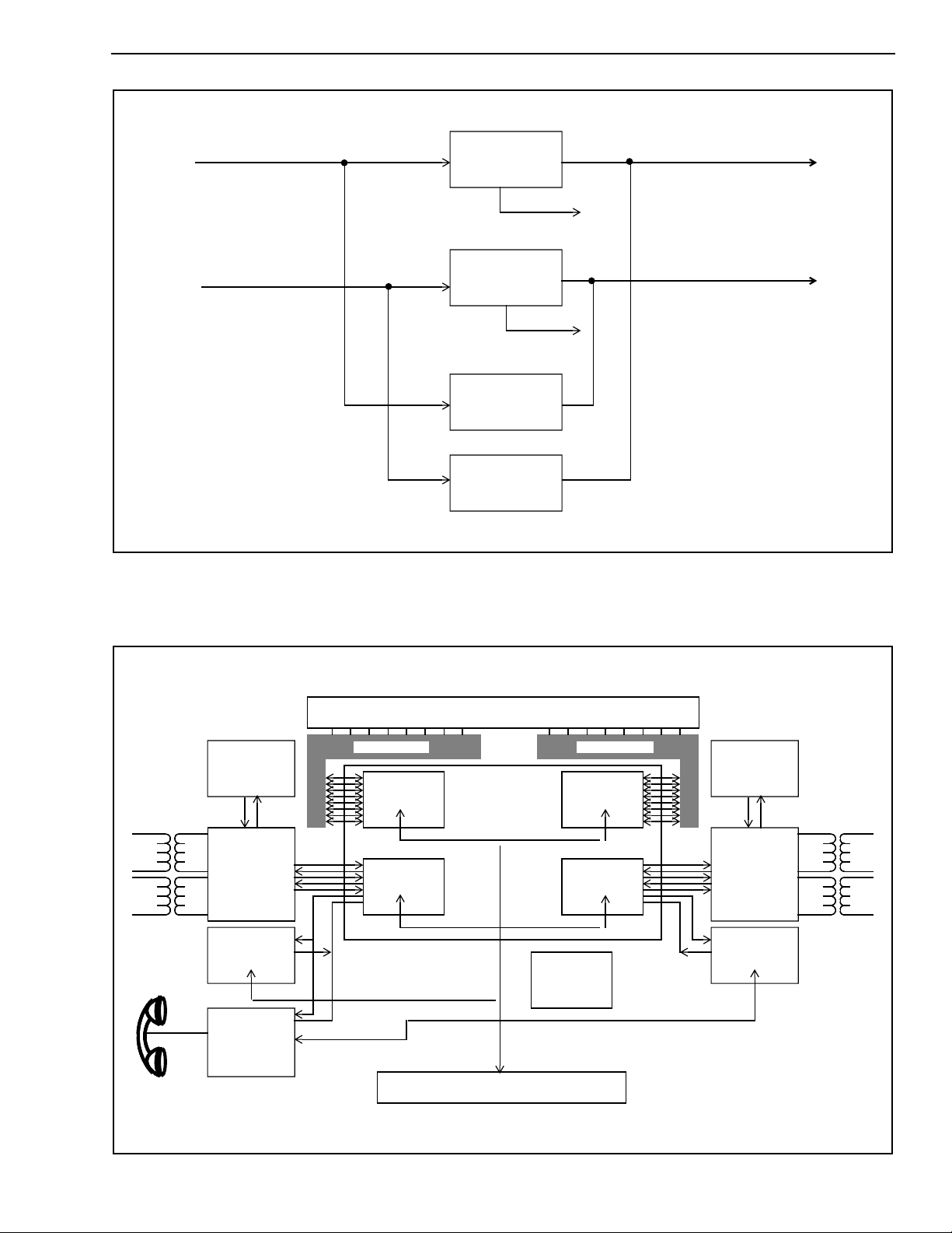
channels has to be maintained. The MT89L85 device
suits this application and can be used to form a
complete non-blocking switch matrix of 512 channels
(see Figure 9). This allows 8 pairs of ST-BUS
streams to be dedicated to the MVIP side whereas
the remaining 8 pairs are used for local ancilliary
functions in typical dual T1/E1 interface applications
(Figure 10).
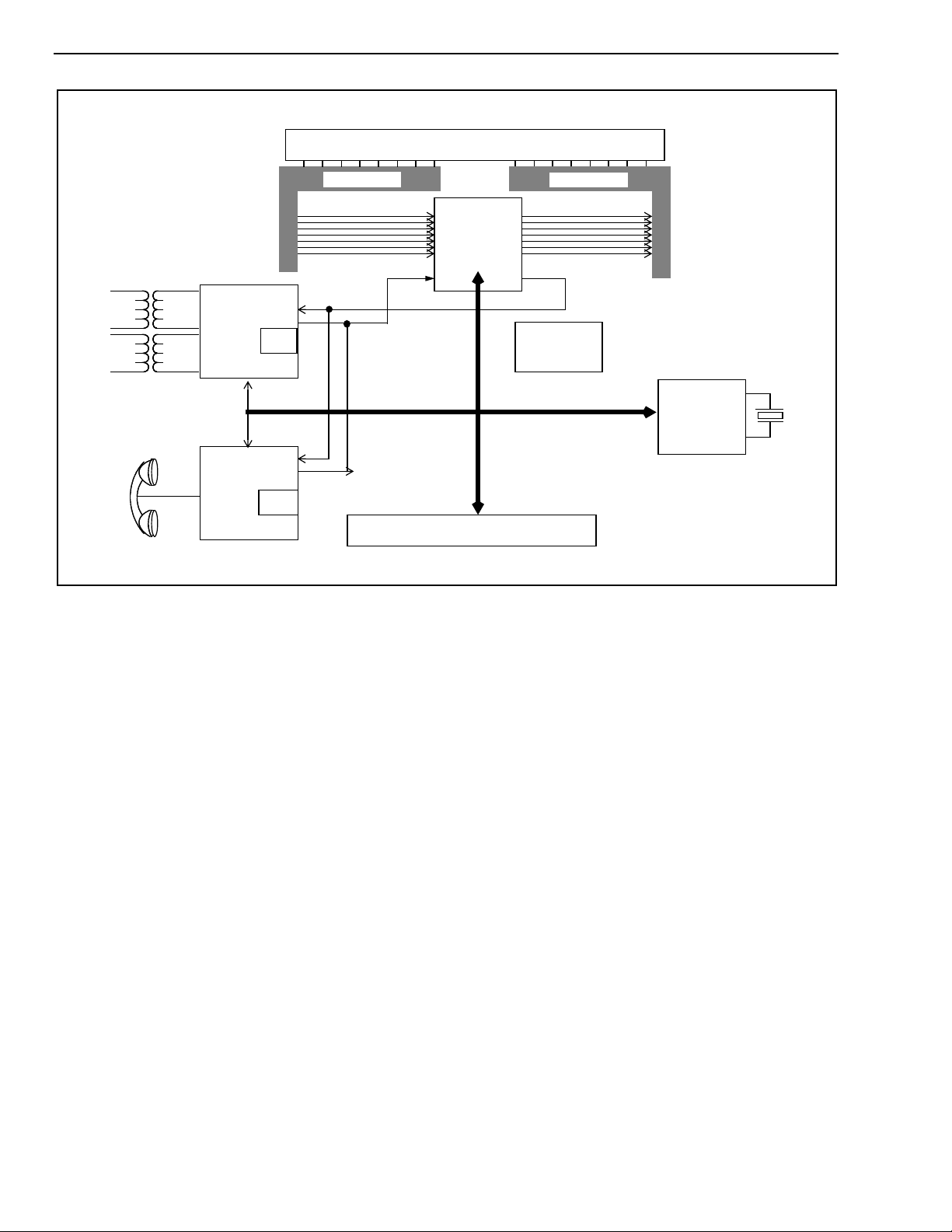
Another application of the MT89L85 in an MVIP
environment is to build an ISDN S-interface card
(Figure 11). In this card, 7 pairs of ST-BUS streams
are connected to the MVIP interface while the
remaining pair is reserved for the interconnection of
MITEL MT8930 (SNIC), MT8992 (H-PHONE) and
the MVIP interface.
9
Page 10
MT89L85 Advance Information
To Video, Data, Fax and other services
MVIP
BUS
Server 1
ISDN
S-Interface
•
•
•
•
•
MT89L85s
(x4)
HDLC
MVIP
BUS
MT89L85
MT89L85
MT89L85
MT89L85
Dual T1/E1 Card
ST-BUS
MH89760B
MH89790B
T1
E1
MH89760B
MH89790B
•
•
•
•
•
•
ST-BUS
Local T1/E1 Link
(256 PORT
SWITCH MODULE) Server 3
MH89760B/790B
MH89760B/790B
MH89760B/790B
Local T1/E1 Link
MT89L85s
(x4)
MT8930B
MT8930B
Server 3
•
•
ST-BUS
MH89760B
MH89790B
Server 2
ST-BUS
MT8972B
or
ANALOG
MT89L85s
(x4)
MVIP
BUS
•
•
•
•
•
To Video, Data,
Fax Services
Local Environment Network Access
Public
Figure 8b - Implementation of an Isochronous Network Using Mitel Components
10
Page 11
Advance Information MT89L85
8 Input Streams
From MVIP
8 Input On-Board
ST-BUS Streams
MT89L85 #1
CSTo
MVIP Direction
MT89L85 #2
CSTo
MVIP Enable
MT89L85
#3
MT89L85
#4
Figure 9 - 512-Channel Switch Array
8 Output Streams
to MVIP
8 Output On-Board
ST-BUS Streams
FDL HDLC
MT8952B
T1/E1
MH89760B
or
MH89790B
HDLC
MT8952B
ANALOG
D-PHONE
MT8992/93
MVIP HEADER
MVIP STo0-7 MVIP STi0-7
SWITCH
MT89L85
SWITCH
MT89L85
512 Channel
Switch Matrix
PC INTERFACE
SWITCH
MT89L85
SWITCH
MT89L85
DPLL
MT8941
FDL HDLC
MT8952B
T1/E1
MH89760B
or
MH89790B
HDLC
MT8952B
Figure 10 - Dual T1/E1 Card Functional Block Diagram
11
Page 12
MT89L85 Advance Information
MVIP HEADER
S
INTERFACE
HDLC
MT8930B
DIGITAL
PHONE
HDLC
MT8992/93
MVIP STo1-7
STi7-1 STo7-1
STi0 STo0
SWITCH
MATRIX
MT89L85
PC INTERFACE
MVIP STi1-7
DPLL
MT8941
Figure 11 - S-Access Card Functional Block Diagram
DTMF
RECEIVER
MT8870
12
Page 13
Advance Information MT89L85
Absolute Maximum Ratings*
Parameter Symbol Min Max Units
1VDD - V
2 Voltage on Digital Inputs V
3 Current at Digital Outputs I
4 Storage Temperature T
5 Package Power Dissipation P
* Exceeding these values may cause permanent damage. Functional operation under these conditions is not implied.
SS
I
O
S
D
Recommended Operating Conditions - Voltages are with respect to ground (V
Characteristics Sym Min Typ
1 Operating Temperature T
2 Positive Supply V
3 Input High Voltage V
4 Input High Voltage on 5V
OP
DD
IH
V
IH
-40 25 +85 °C
3.0 3.3 3.6 V
0.7V
DD
‡
Max Units Test Conditions
V
DD
5.5 V
-0.3 5.0 V
VSS-0.3 VDD+0.3 V
-55 +125 °C
) unless otherwise stated.
SS
V
Tolerant Inputs
5 Input Low Voltage V
‡ Typical figures are at 25°C and are for design aid only: not guaranteed and not subject to production testing.
IL
DC Electrical Characteristics - Voltages are with respect to ground (V
Characteristics Sym Min Typ
V
SS
0.3V
DD
) unless otherwise stated.
SS
‡
Max Units Test Conditions
V
20 mA
1W
1
2 Input High Voltage V
3 Input Low Voltage V
4 Input Leakage I
5 Input Pin Capacitance C
6
7 Output High Current I
8 Output Low Voltage V
9 Output Low Current I
10 High Impedance Leakage I
11 Output Pin Capacitance C
‡ Typical figures are at 25°C and are for design aid only: not guaranteed and not subject to production testing.
*
Supply Current I
I
N
P
U
T
S
Output High Voltage V
O
U
T
P
U
T
S
DD
OH
OZ
IH
IL
OH
OL
OL
4 7 mA Outputs unloaded
0.7V
DD
IL
0.3V
DD
V
V
5 µAVI between VSS and V
I
0.8V
DD
10 pF
VIOH = 10 mA
10 mA Sourcing. VOH=0.8V
0.4 V IOL = 5 mA
5 mA Sinking. VOL = 0.4V
5 µAVO between VSS and V
O
10 pF
AC Electrical Characteristics _Timing Parameter Measurement Voltage Levels
Characteristics Sym Level Units Test Conditions
1 CMOS Threshold Voltage V
2 CMOS Rise/Fall Threshold Voltage high V
3 CMOS Rise/Fall Threshold Voltage low V
TT
HM
LM
0.5V
0.7V
0.3V
DD
DD
DD
V
V
V
DD
DD
DD
13
Page 14
MT89L85 Advance Information
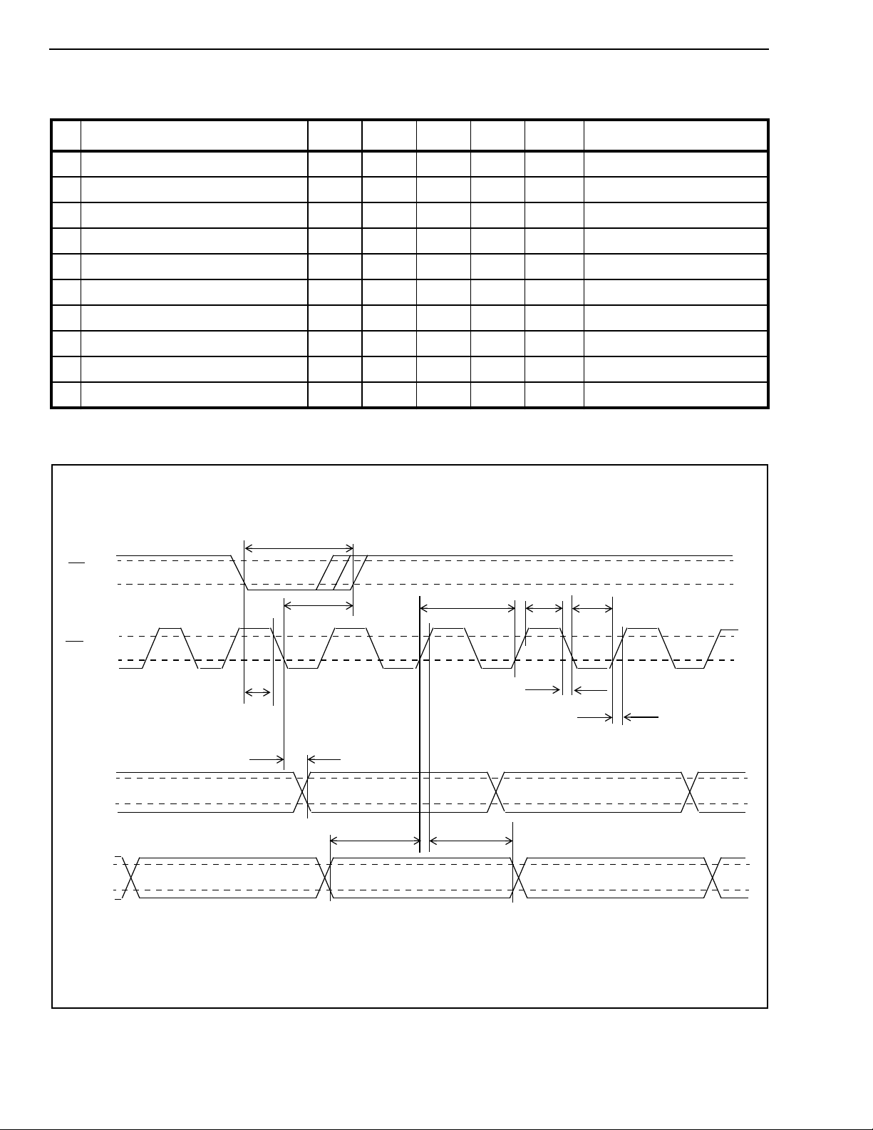
AC Electrical Characteristics† - ST-BUS Timing
Voltages are with respect to ground (VSS) unless otherwise stated.
Characteristics Sym Min Typ
‡
Max Units Test Conditions
1 Frame Pulse width t
2 Frame Pulse setup time t
3 Frame Pulse hold time t
4 STo delay Active to Active t
5 STi setup time t
6 STi hold time t
7 Clock period
8 CK Input Low t
9 CK Input High
10 Clock Rise/Fall Time tr,t
† Timing is over recommended temperature & power supply voltages (VDD=5V±5%, VSS=0V, TA=–40 to 85°C).
‡ Typical figures are at 25°C and are for design aid only: not guaranteed and not subject to production testing.
V
HM
F0i
V
LM
t
F0iW
t
F0iH
F0iW
F0iS
F0iH
SAA
STiS
STiH
t
C4i
CL
t
CH
10 190 ns
20 190 ns
20 ns
20 ns
200 244 300 ns
85 122 150 ns
85 122 150 ns
f
244 ns
55 ns CL=150 pF
10 ns
t
C4i
t
CH
t
CL
C4i
STo
STi
V
HM
V
LM
t
t
F0iS
t
DAA
V
HM
V
LM
V
HM
V
LM
Ch. 31
Bit 0
Ch. 31
Bit 0
Ch. 0
Bit 7
t
STiS
Ch. 0
Bit 7
t
STiH
f
t
r
Ch. 0
Bit 6
Ch. 0
Bit 6
Ch. 0
Bit 5
Ch. 0
Bit 5
Figure 12 - ST-BUS Timing
14
Page 15
Advance Information MT89L85
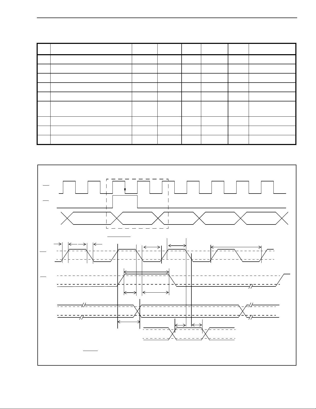
AC Electrical Characteristics† - GCI Timing
Voltages are with respect to ground (VSS) unless otherwise stated.
Characteristics Sym Min Typ
‡
Max Units Test Conditions
1 Clock Period t
C4i
2 Pulse Width tCL, t
3 Frame Width High t
4 Frame Setup t
5 Frame Hold t
6 Data Delay/Clock Active to
WFH
F0iS
F0iH
t
DAA
CH
150 244 300 ns
73 122 150 ns
244 ns
10 190 ns
20 190 ns
55 ns CL=150 pF
Active
7 Serial Input Setup t
8 Serial Input Hold t
9 Clock Rise/Fall Time tr,t
† Timing is over recommended temperature & power supply voltages (VDD=3.3V±5%, VSS=0V, TA=–40 to 85°C).
‡ Typical figures are at 25°C and are for design aid only: not guaranteed and not subject to production testing.
C4i
F0i
STiS
STiH
f
20 ns
20 ns
10 ns
C4i
F0i
STo
STi
STi/
STo
bit 0 bit 1 bit 2 bit 3
See Detail a
t
r
V
HM
V
LM
V
HM
V
LM
V
HM
V
LM
V
HM
V
LM
t
f
Detail a
t
DAA
t
F0iS
t
t
t
F0iH
CL
WFH
Note: bit 0 identifies the first bit of the GCI frame
t
CH
t
STiS
t
STiH
t
C4i
Figure 13 - GCI Timing
15
Page 16
MT89L85 Advance Information
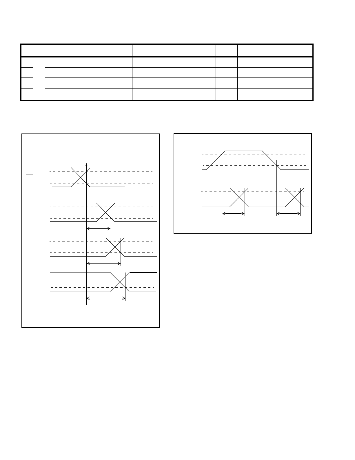
AC Electrical Characteristics† - Serial Streams for ST-BUS and GCI Backplanes
ODE
STo0
to
STo7
‡
Max Units Test Conditions
55 ns RL=1 KΩ*, CL=150 pF
55 ns CL=150 pF
50 ns RL=1 KΩ*, CL=150 pF
55 ns CL=150 pF
V
HM
V
LM
V
HM
LM
*
t
OED
t
OED
V
*
Characteristics Sym Min Typ
O
1
2 STo0/7 Delay - High Z to Active t
3 Output Driver Enable Delay t
4 CSTo Output Delay t
† Timing is over recommended temperature & power supply voltages.
‡ Typical figures are at 25°C and are for design aid only: not guaranteed and not subject to production testing.
* High Impedance is measured by pulling to the appropriate rail with RL, with timing corrected to cancel time taken to discharge CL.
C4i
STo0
to
STo7
STo0/7 Delay - Active to High Z t
U
T
P
U
T
S
Bit Cell Boundary
V
HM
V
LM
V
HM
V
LM
SAZ
SZA
OED
XCD
(GCI)
(ST-BUS)
*
t
SAZ
V
STo0
to
STo7
CSTo
HM
V
LM
V
HM
V
LM
*
t
SZA
t
XCD
Figure 14 - Serial Outputs and External Control
Figure 15 - Output Driver Enable
16
Page 17
Advance Information MT89L85
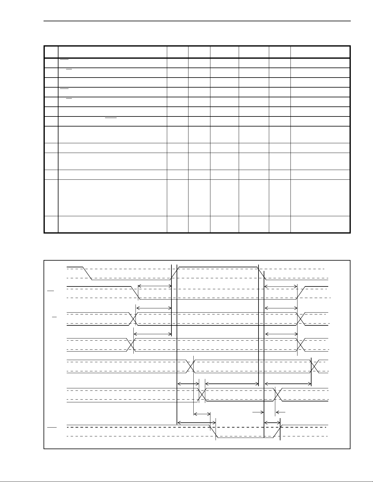
AC Electrical Characteristics†- Microprocessor Bus
Voltages are with respect to ground (VSS) unless otherwise stated .
Characteristics Sym Min Typ
‡
Max Units Test Conditions
1 CS Setup from DS rising t
2R/W Setup from DS rising t
3 Add setup from DS rising t
4 CS hold after DS falling t
5R/W hold after DS falling t
6 Add hold after DS falling t
7 Data setup from DTA Low on Read t
8 Data hold on read
CSS
RWS
ADS
CSH
RWH
ADH
DDR
t
DHR
0ns
5ns
5ns
0ns
5ns
8ns
0ns C
=150 pF
L
10 90 ns RL=1 KΩ*,
CL=150 pF
9 Data setup on write (fast write) t
10 Valid Data Delay on write
DSW
t
SWD
025 ns
122 ns
(slow write)
11 Data hold on write t
12 Acknowledgment Delay:
Reading Data Memory
Reading/Writing Conn. Memory
Writing to Control Register
Reading Control Register
13 Acknowledgment Hold Time t
DHW
t
AKD
AKH
510 ns
CL=150 pF
560
62/30
25
52
1220
120/53
65
120
ns
ns
ns
ns
50 80 ns RL=1 KΩ*,
CL=150 pF
† Timing is over recommended temperature & power supply voltages .
‡ Typical figures are at 25°C and are for design aid only: not guaranteed and not subject to production testing.
* High Impedance is measured by pulling to the appropriate rail with RL, with timing corrected to cancel time taken to discharge CL.
DS
CS
R/
W
A0-A6
D0-D7
READ
D0-D7
WRITE
DTA
t
CSS
t
RWS
t
ADS
t
SWD
t
AKD
t
DDR
VALID DATA
t
DSW
VALID DATA
t
DHW
t
AKH
t
CSH
t
RWH
t
ADH
t
DHR
V
HM
V
LM
V
HM
V
LM
V
HM
V
LM
V
HM
V
LM
V
HM
V
LM
V
HM
V
LM
V
HM
V
LM
Figure 16 - Motorola Non-Multiplexed Bus Timing
17
Page 18
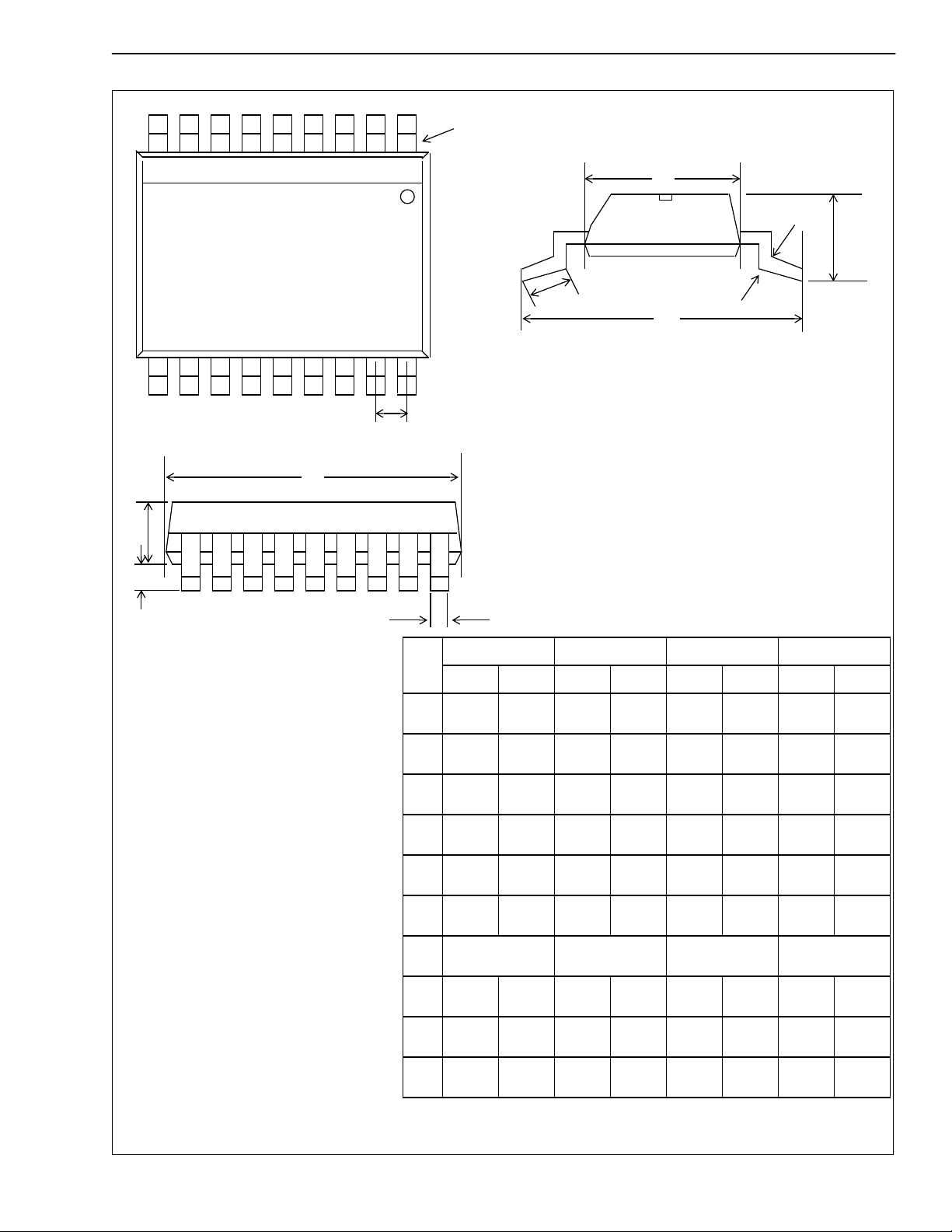
Pin 1
Package Outlines
E
A
L
H
e
D
A
2
A
1
B
Notes:
1) Not to scale
2) Dimensions in inches
3) (Dimensions in millimeters)
4) Ref. JEDEC Standard M0-150/M0118 for 48 Pin
5) A & B Maximum dimensions include allowable mold flash
C
20-Pin 24-Pin 28-Pin 48-Pin
Dim
Min Max Min Max Min Max Min Max
A 0.079
(2)
A10.002
(0.05)
B 0.0087
(0.22)
C 0.008
D 0.27
(6.9)
E 0.2
(5.0)
e 0.025 BSC
A20.065
(1.65)
H 0.29
(7.4)
L 0.022
(0.55)
0.013
(0.33)
(0.21)
0.295
(7.5)
0.22
(5.6)
(0.635 BSC)
0.073
(1.85)
0.32
(8.2)
0.037
(0.95)
- 0.079
0.002
(0.05)
0.0087
(0.22)
0.31
(7.9)
0.2
(5.0)
0.025 BSC
(0.635 BSC)
0.065
(1.65)
0.29
(7.4)
0.022
(0.55)
(2)
0.013
(0.33)
0.008
(0.21)
0.33
(8.5)
0.22
(5.6)
0.073
(1.85)
0.32
(8.2)
0.037
(0.95)
0.002
(0.05)
0.0087
(0.22)
0.39
(9.9)
0.2
(5.0)
0.025 BSC
(0.635 BSC)
0.065
(1.65)
0.29
(7.4)
0.022
(0.55)
0.079
(2)
0.013
(0.33)
0.008
(0.21)
0.42
(10.5)
0.22
(5.6)
0.073
(1.85)
0.32
(8.2)
0.037
(0.95)
0.095
(2.41)
0.008
(0.2)
0.008
(0.2)
0.62
(15.75)
0.291
(7.39)
0.025 BSC
(0.635 BSC)
0.089
(2.26)
0.395
(10.03)
0.02
(0.51)
0.110
(2.79)
0.016
(0.406)
0.0135
(0.342)
0.010
(0.25)
0.63
(16.00)
0.299
(7.59)
0.099
(2.52)
0.42
(10.67)
0.04
(1.02)
Small Shrink Outline Package (SSOP) - N Suffix
General-11
Page 19
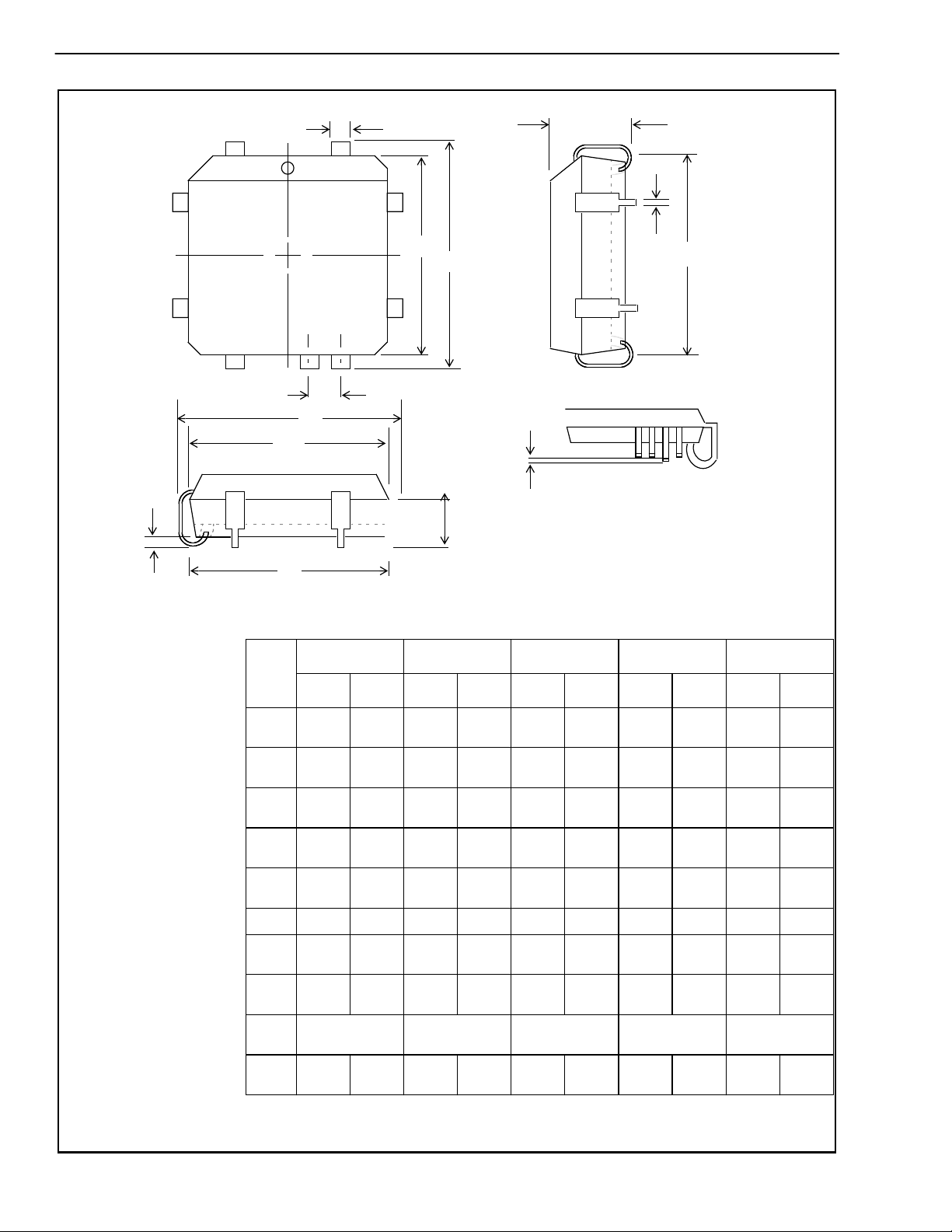
Package Outlines
F
D
1
D
H
E
E
1
e: (lead coplanarity)
A
1
I
E
2
Notes:
1) Not to scale
2) Dimensions in inches
3) (Dimensions in millimeters)
4) For D & E add for allowable Mold Protrusion 0.010"
A
G
D
2
Dim
A
A
D/E
D1/E
D2/E
e
F
G
H
I
20-Pin 28-Pin 44-Pin 68-Pin 84-Pin
Min Max Min Max Min Max Min Max Min Max
0.165
(4.20)
0.090
1
(2.29)
0.385
(9.78)
0.350
1
(8.890)
0.290
2
(7.37)
0.026
(0.661)
0.013
(0.331)
0.020
(0.51)
0.180
(4.57)
0.120
(3.04)
0.395
(10.03)
0.356
(9.042)
0.330
(8.38)
0 0.004 0 0.004 0 0.004 0 0.004 0 0.004
0.032
(0.812)
0.021
(0.533)
0.050 BSC
(1.27 BSC)
0.165
(4.20)
0.090
(2.29)
0.485
(12.32)
0.450
(11.430)
0.390
(9.91)
0.026
(0.661)
0.013
(0.331)
0.050 BSC
(1.27 BSC)
0.020
(0.51)
0.180
(4.57)
0.120
(3.04)
0.495
(12.57)
0.456
(11.582)
0.430
(10.92)
0.032
(0.812)
0.021
(0.533)
0.165
(4.20)
0.090
(2.29)
0.685
(17.40)
0.650
(16.510)
0.590
(14.99)
0.026
(0.661)
0.013
(0.331)
0.050 BSC
(1.27 BSC)
0.020
(0.51)
0.180
(4.57)
0.120
(3.04)
0.695
(17.65)
0.656
(16.662)
0.630
(16.00)
0.032
(0.812)
0.021
(0.533)
0.165
(4.20)
0.090
(2.29)
0.985
(25.02)
0.950
(24.130)
0.890
(22.61)
0.026
(0.661)
0.013
(0.331)
0.050 BSC
(1.27 BSC)
0.020
(0.51)
0.200
(5.08)
0.130
(3.30)
0.995
(25.27)
0.958
(24.333)
0.930
(23.62)
0.032
(0.812)
0.021
(0.533)
(30.10)
(29.210)
(27.69)
(0.661)
(0.331)
0.165
(4.20)
0.090
(2.29)
1.185
1.150
1.090
0.026
0.013
0.050 BSC
(1.27 BSC)
0.020
(0.51)
0.200
(5.08)
0.130
(3.30)
1.195
(30.35)
1.158
(29.413)
1.130
(28.70)
0.032
(0.812)
0.021
(0.533)
General-10
Plastic J-Lead Chip Carrier - P-Suffix
Page 20

http://www.mitelsemi.com
World Headquarters - Canada
Tel: +1 (613) 592 2122
Fax: +1 (613) 592 6909
North America Asia/Pacific Europe, Middle East,
Tel: +1 (770) 486 0194 Tel: +65 333 6193 and Africa (EMEA)
Fax: +1 (770) 631 8213 Fax: +65 333 6192 Tel: +44 (0) 1793 518528
Fax: +44 (0) 1793 518581
Information relating to products and services furnished herein by Mitel Corporation or its subsidiaries (collectively “Mitel”) is believed to be reliable. However, Mitel assumes no
liability for errors that may appear in this publication, or for liability otherwise arising from the application or use of any such information, product or service or for any infringement of
patents or other intellectual property rights owned by third parties which may result from such application or use. Neither the supply of such information or purchase of product or
service conveys any license, either express or implied, under patents or other intellectual property rights owned by Mitel or licensed from third parties by Mitel, whatsoever.
Purchasers of products are also hereby notified that the use of product in certain ways or in combination with Mitel, or non-Mitel furnished goods or services may infringe patents or
other intellectual property rights owned by Mitel.
This publication is issued to provide information only and (unless agreed by Mitel in writing) may not be used, applied or reproduced for any purpose nor form part of any order or
contract nor to be regarded as a representation relating to the products or services concerned. The products, their specifications, services and other information appearing in this
publication are subject to change by Mitel without notice. No warranty or guarantee express or implied is made regarding the capability, performance or suitability of any product or
service. Information concerning possible methods of use is provided as a guide only and does not constitute any guarantee that such methods of use will be satisfactory in a specific
piece of equipment. It is the user’s responsibility to fully determine the performance and suitability of any equipment using such information and to ensure that any publication or
data used is up to date and has not been superseded. Manufacturing does not necessarily include testing of all functions or parameters. These products are not suitable for use in
any medical products whose failure to perform may result in significant injury or death to the user. All products and materials are sold and services provided subject to Mitel’s
conditions of sale which are available on request.
M Mitel (design) and ST-BUS are registered trademarks of MITEL Cor poration
Mitel Semiconductor is an ISO 9001 Registered Company
Copyright 1999 MITEL Corporation
All Rights Reserved
Printed in CANADA
TECHNICAL DOCUMENTATION - NOT FOR RESALE
 Loading...