

Page 1
MT9042
Global Digital Trunk Synchronizer
Preliminary Info rmatio n
Features
• Provides T1 and E1 clocks, and ST-BUS/GCI
framing sign als loc ked t o an in put refe renc e of
either 8 kHz (fram e pulse ), 1.54 4 MH z (T1) , or
2.048 MHz (E 1)
• Meets AT & T TR62411 and ETSI ETS 300 011
specificatio ns for a 1.544 M Hz (T1), or
2.048 MHz (E 1) in put refe renc e
• Provides Time Interval Error (T IE) corre ction to
suppress input refe renc e rearran gem ent
transient s
• Typical unfiltered intrinsic output jitter is
0.013 UI peak -to- peak
• Jitter attenuation of 15 dB @ 10 Hz,
34 dB @ 100 Hz a nd 5 0 dB @ 5 to 40 k Hz
• Low power CM OS tech nolog y
Applications
• Synchronization and timing control for T1 and
E1 digital transmission links
• ST-BUS clock and f rame pulse s ource s
• Primary Trunk Rate Converters
ISSUE 1 June 1994
Ordering Information
MT9042AP 28 Pin PLCC
°
C to +85°C
-40
Description
The MT9042 is a digital phase-locked loop (PLL)
designed to provide timing and synchronization
signals for T1 and E1 primary rate transmission links
that are compatible with ST-BUS/GCI frame
alignment timing requirements. The PLL outputs can
be synchronized to either a 2.048 MHz, 1.544 MHz,
or 8 kHz reference. The T1 and E1 outputs are fully
compliant with AT & T TR62411 (ACCUNET
and ETSI ETS 300 011 intrinsic jitter and jitter
transfer specifications, respectively, when
synchronized to primary reference input clock rates
of either 1.544 MHz or 2.048 MHz.
The PLL also provides additional high speed output
clocks at rates of 3.088 MHz, 4.096 MHz, 8.192
MHz, and 16.384 MHz for backplane synchronization.
®
T1.5)
RST
PRI
SEC
RSEL
LOSS1
LOSS2
VDD VSS TRST
Reference
Select
MUX
Automatic State
Machine
MS1 MS2GTo GTi
TIE
Corrector
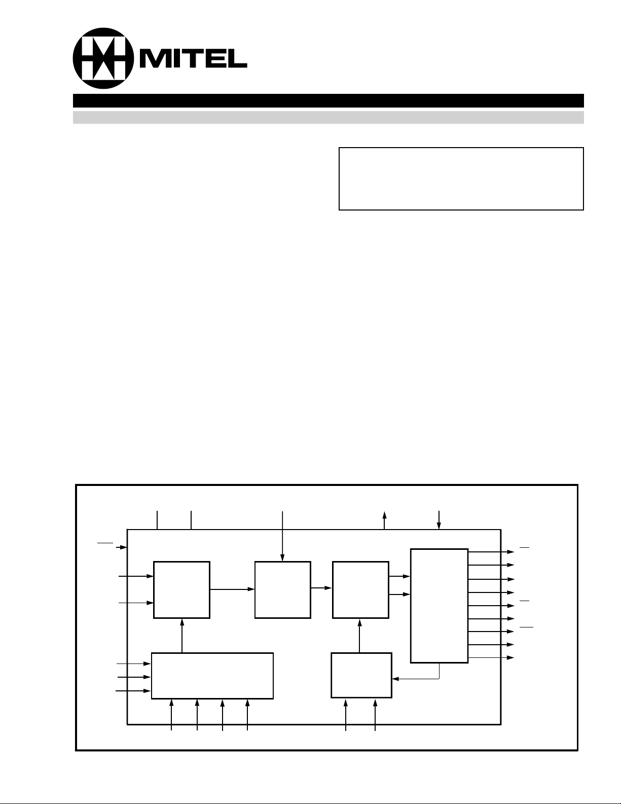
Figure 1 - Functional Block Diagram
FSEL1
MCLKo MCLKi
PLL
Divider
FSEL2
Interface
Circuit
C3
C1.5
C16
C8
C4
C2
F0o
FP8-STB
FP8-GCI
3-97
Page 2
MT9042 Preliminary Information
VSS
TRST
SEC
PRI
RST
FSEL2
FSEL1
432
VDD
MCLKo
MCLKi
FP8-GCI
F0o
FP8-STB
C1.5 GTi
5
6
7
8
9
10
11
12 13 14 15 16 17 18
C3
C2
1
C4
VSS
C8
262728
25
RSEL
24
MS1
23
MS2
22
LOSS1
21
LOSS2
20
GTo
19
C16
VDD
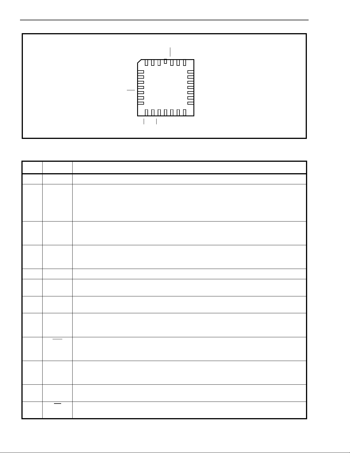
Figure 2 - Pin Connections
Pin Description
Pin # Name Description
1V
2 TRST TIE Circuit Reset (TTL compatible). When HIGH, the time interval error correction circuit is
3 SEC Secondary Referen ce In put (TT L comp atible). This input (either 8 kHz, 1.544 MHz, or
Negative Power Supply V oltage. Nominally 0 Volts.
SS
alternately establishing the phase differe nce betwee n the PRI and SEC ref erence input s,
depending upon which input is selected as input for PLL synchronization. This information is
used to generate a virtual reference for input to the PLL. When LOW, the time interval error
correction circuit is bypassed.
2.048 MHz as controlled by the input frequen c y selection pins) is used as an alternat e
reference source for PLL synchronization.
4PRIPrimary Reference Input (TTL compatible). This input (either 8 kHz, 1.544 MHz, or 2.048
MHz as controlled by the input frequency selection pins) is used as the primary reference
source for PLL synchronization.
5V
DD
Positive Supply Voltage. Nominally +5 volts.
6MCLKoMaster Clock Oscillator Output. This is a CMOS buffered output used for driving a 20 MHz
crystal.
7MCLKiMaster Clock Osc illato r Input. This is a CMOS input for a 20 MHz crystal or crystal
oscillator. Signals should be DC coupled to this pin.
8 FP8-GCI Frame Pulse Outpu t (CMOS com p atib le). This is an 8 kHz output framing pulse th at
indicates the start of the active GCI-BUS frame. The pulse width is based upon the period of
the 8.192 MHz synchronization clock.
9F0o
Frame Pulse Outpu t (CMOS com p atib le). This is an 8 kHz output framing pulse th at
indicates the start of the active ST-BUS frame. The pulse width is based upon the period of
the 4.096 MHz synchronization clock. This is an active low signal.
10 FP8-STB Fram e Puls e Outpu t (CMOS comp atib le ). This is an 8 kHz output framing pulse th at
indicates the start of the active ST-BUS frame. The pulse width is based upon the period of
the 8.192 MHz synchronization clock.
11 C1.5 Clock 1.544 MHz (CMOS compatible). This ouput is a 1.544 MHz (T1) output clock locked
to the selected reference input signal.
12 C3
Clock 3.088 MH z (CMOS compa tibl e). This output is a 3.088 MHz output clock locked to
the selected reference input signal.
3-98
Page 3
Preliminary Information MT9042
Pin Description (continued)
Pin # Name Description
13 C2 Clock 2.048 MHz (CMOS compatible). This output is a 2.048 MHz (E1) output clock
locked to the selected reference input signal.
14 C4
Clock 4.096 MHz (CMOS compatible). This output is a 4.096 MHz output clo ck locked to
the selected reference input signal.
15 V
Negative Power Supply Voltage. Nominally 0 Volts.
SS
16 C8 Clock 8.192 MHz (CMOS compatible). This output is an 8.192 MHz output clock locked to
the selected reference input signal.
17 C16 Clock 16.384 MHz (CMOS compatible). This output is a 16.384 MHz output clock locked
to the selected reference input signal.
18 V
Positive Supply Voltage. Nominally +5 volts.
DD
19 GTi Guard Time Input (TTL Level Schmitt Trigger). This TTL level Schmitt trigger input is
used to determine the threshold level of the RC generated (guard) time const ant. Thi s
function filters out unwanted rearrangeme nts bet ween the PRI and SEC reference input
signals.
20 GTo Guard Time Output (CMOS compatible). This is a CMOS buffered output used to drive the
external RC generated (guard) time constant circuit.
21 LOSS2 Reference Loss Indicator - 2 Input (TTL compatib le). This input, in conjunction with
LOSS1, comprises a set of signals which control the event driven state machine when the
PLL is operating in AUTOMATIC mode (see Ta ble 4 ).
22 LOSS1 Reference Loss Indicator - 1 Input (TTL compatib le). This input, in conjunction with
LOSS2, comprises a set of signals which control the event driven state machine when the
PLL is operating in AUTOMATIC mode (see Ta ble 4 ).
23 MS2 Mode Select - 2 Input (TTL co mpati bl e). This input, in conjunctio n with MS1, select s the
PLL mode of operation (i.e.,NORMAL, HOLDOVER, FREERUN, or AUTOMATIC; see Table
1).
24 MS1 Mode Select - 1 Input (TTL co mpati bl e). This input, in conjunctio n with MS2, select s the
PLL mode of operation (i.e., NORMAL, HOLDOVER, FREERUN, or AUTOMATIC; see Table
1).
25 RSEL Input Reference Select (TTL compatible). When LOW this input selects PRI as the
reference input signal, and when HIGH, selects SEC as the reference input signal (see Table
2).
26 FSEL2 Frequ enc y Select - 2 Input (TTL com p ati ble ). This input, in conjunction with FSEL1,
selects the frequency of the input refere nce source (i.e., 8 kHz, 1.544 MH z, or 2.048 MHz;
see Table 3).
27 FSEL1 Frequ enc y Select - 1 Input (TTL com p ati ble ). This input, in conjunction with FSEL2,
selects the frequency of the input refere nce source (i.e., 8 kHz, 1.544 MH z, or 2.048 MHz;
see Table 3).
28 RST
Reset (TTL compatible). This input (active LOW) puts the MT9042 in its reset state. To
guarantee proper operation, the device must be reset after power-up. The time constant for
a power-up reset circuit must be a minimum of five times the rise time of the power supply. In
normal operation, the RST
pin must be held low for a minimum of 60 nsec to reset the
device.
3-99
Page 4
MT9042 Preliminary Information
Functional Description
The MT9042 is a fully digital, phase-locked loop
designed to provide timing references to interface
circuits for T1 and E1 Primary Rate Digital
Transmission links. As shown in Figure 1, the PLL
consists of an input reference selection circuit (MUX),
a Time Interval Error corrector (TIE), and a PLL that
employs a high resolution Digitally Controlled
Oscillator (DCO) to generate the T1 and E1 outputs.
The MT9042 accepts two reference clock inputs,
primary (PRI) and secondary (SEC) both connected
to independent external reference sources, eit her of
which can be selected as reference for
synchronization by the reference select (RSEL)
input. The selected reference signal is then
regenerated by the TIE correction circuit and passed
as a virtual reference to the PLL. The TIE correction
circuit will limit phase jumps (as specified by AT & T
TR62411 and ETSI ETS 300 011) during
rearrangement between the external reference
clocks. This virtual reference is then used by the
PLL for synchronizing the output signals.
Modes of Operation
The MT9042 can operate in one of two modes,
MANUAL or AUTOMATIC, as controlled by mode
select pins MS1 and MS2 (see Table 1). In MANUAL
mode, the user is responsible for switching
references during NORMAL operation, as well as
forcing the PLL into FREERUN or HOLDOVER
states.
When AUTOMATIC mode is selected, operation is
controlled by an internal state machine. Under state
machine control, input reference selection is
automatically based upon the input levels of LOSS1
and LOSS2.
MS2 MS1 D escription of Operation
0 0 NORMAL (manual mode)
0 1 HOLDOVER (manual mode)
1 0 FREERUN (manual mode)
11AUTOMATIC MODE
The interface circuit on the output of the DCO
generates 1.544 MHz (C1.5), 3.088 MHz (C3
MHz (C2), 4.096 MHz (C4
), 8.192 MHz (C8), 16.384
MHz (C16), and three 8 kHz frame pulses F0o
), 2.048
, FP8-
STB, and FP8-GCI.
Phase
Detector
f
ref
Loop
Filter
Divider
DCO
f
sync
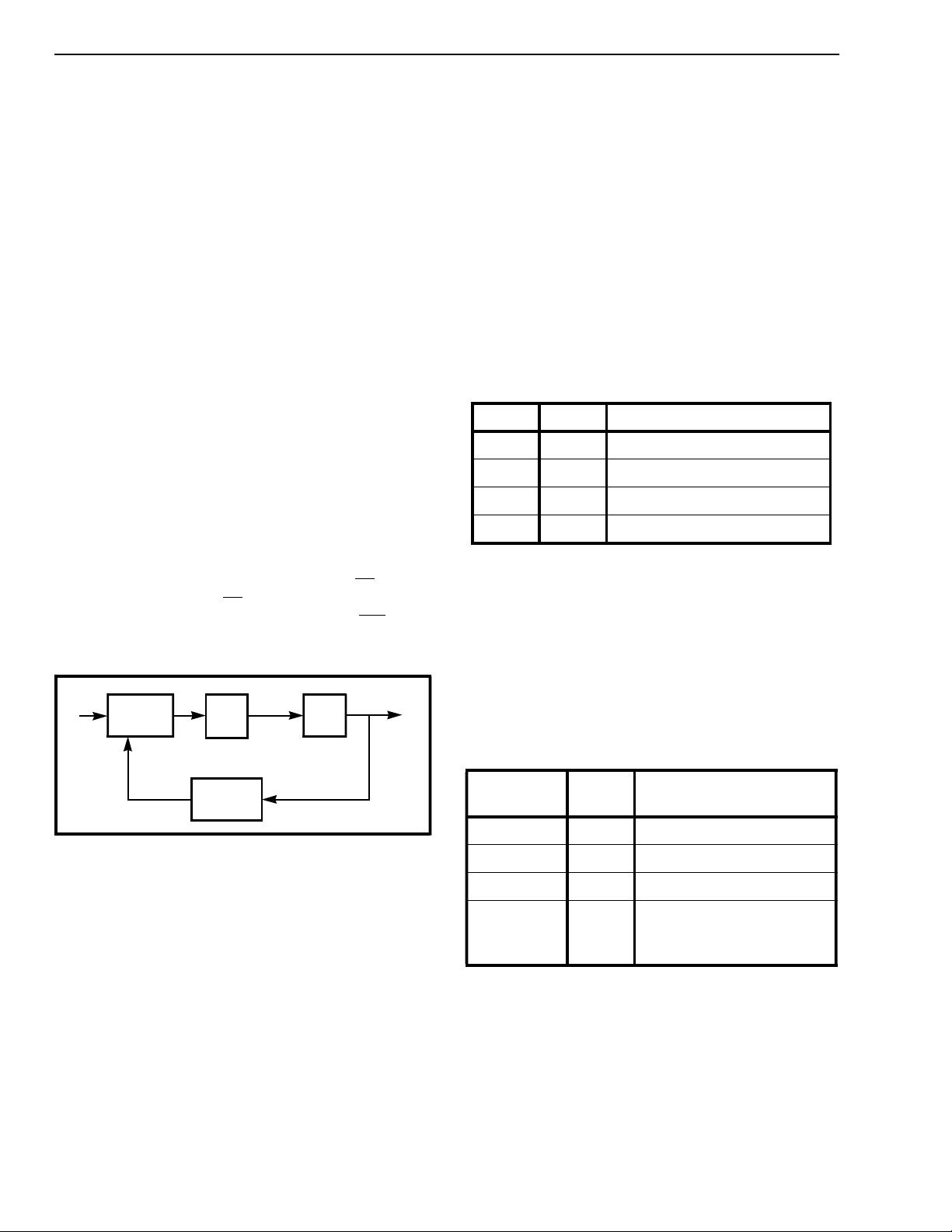
Figur e 3 - PL L Blo ck Diag ra m
As shown in Figure 3, the PLL of the MT9042
consists of a phase detector (PD), a loop filter, a high
resolution DCO, and a digital frequency divider. The
digitally controlled oscillator (DCO) is locked in
frequency (n x f
) to one of three possible reference
ref
frequencies, configured using pins FSEL1 and
FSEL2. Combined with the reference select input
RSEL, the PLL is capable of providing a full range of
E1/T1 clock signals synchronized to either the
primary PRI or secondary SEC input. The loop filter
is a first order lowpass structure that provides
approximately a 2 Hz bandwidth.
Table 3- Operating M odes of the MT9 0 42
Manual Mode
In MANUAL mode operation, the input reference
selection is accomplished through a 2-to-1
multiplexer, which is controlled by the RSEL input
pin. As shown in Table 2, for MANUAL mode
operation RSEL=0 selects PRI as the primary
reference input, while RSEL=1 selects SEC as the
primary reference input .
Mode RSEL Reference Input
Selected
Manual 0 PRI
Manual 1 SEC
Automatic 0 state machine control
Automatic 1 state machine control, but
treats SE C as primary
and PRI as secondary
Ta ble 4- Reference Inpu t Selecti on of the MT904 2
There are three possible input frequencies for
selection as the primary reference clock. These are 8
kHz, 1.544 MHz or 2.048 MHz. Frequency selection
is controlled by the logic levels of FSEL1 and FSEL2,
as shown in Table 3. This variety of input frequencies
was chosen to allow the generation of all the
necessary T1 and E1 clocks from either a T1, E1 or
frame pulse reference source.
3-100
Page 5
Preliminary Information MT9042
Automatic M o d e
In normal AUTOMATIC mode operation, the RSEL
input is set to 0. This will allow the state machin e to
control PLL operation and select the reference input
based on the state of the LOSS1 and LOSS2 inputs
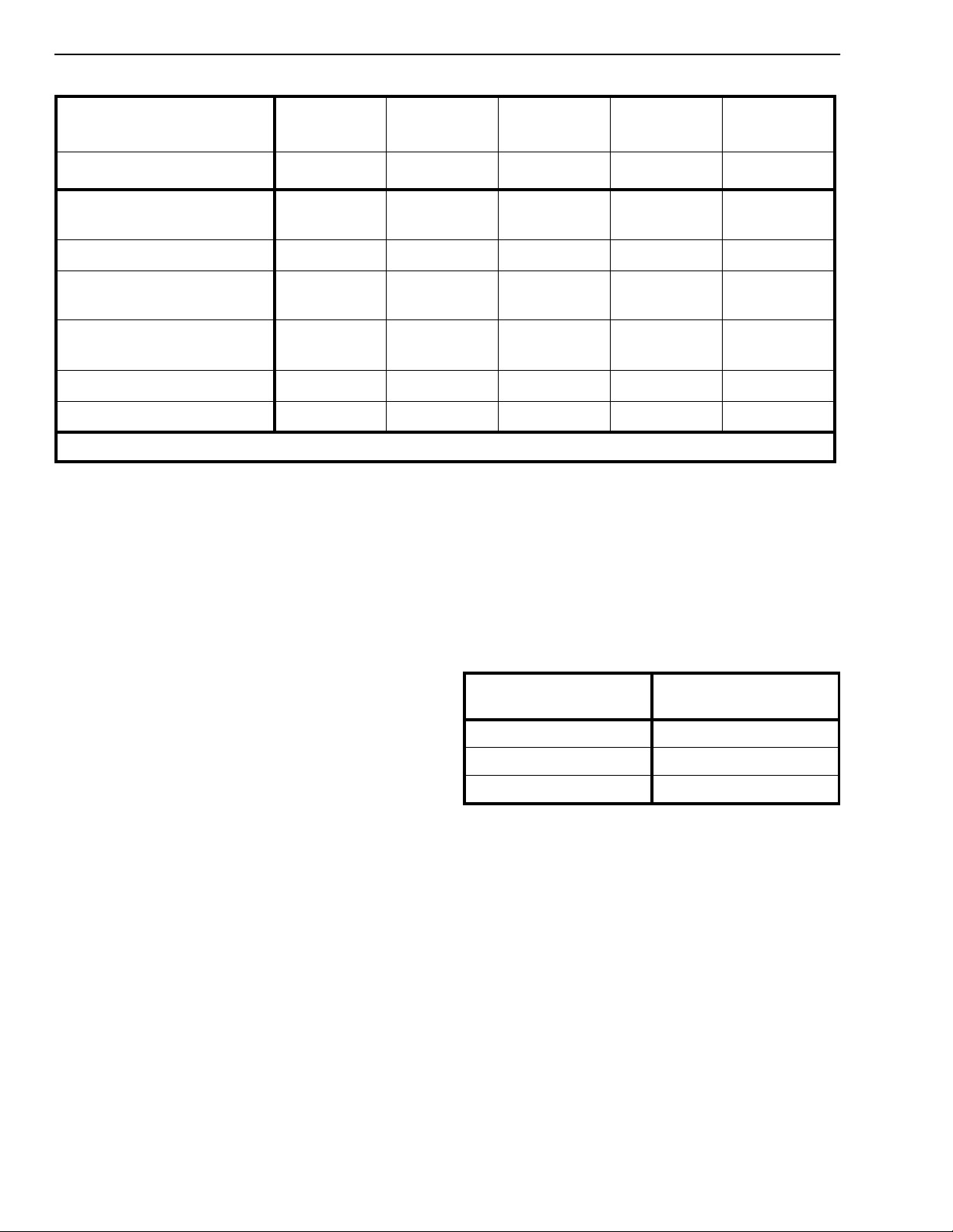
(see state transitions in Table 4). If the PRI reference
signal is lost (LOSS1 = HIGH, LOSS2 = LOW), then
the PLL will enter HOLDOVER mode immediately
and stay there for a time determined by the RC time
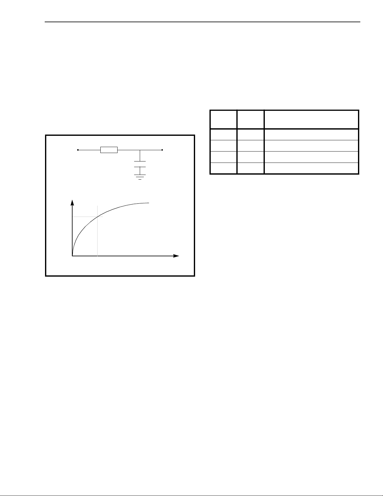
constant connected to the Guard Time input (GTi,
GTo).
R (Ω)
GTo
(a)
V
GTi
1.77v
t
gt
(b)
Figure 4 - a) RC circuit for guard tim e,
b) exponential wavefo rm on GTi
When the primary reference signal has not been
regained and the guard time has been exceeded, the
reference will be switched to SEC. The time
constant determined by the RC circuit connected to
the GTi input provides the hysteresis on automatic
switching between PRI and SEC during very short
interruptions of the primary reference signal. The
Guard Time, t
response of an RC network. The capacitor voltage
on the RC circuit is described by an exponential
curve. When the capacitor voltage reaches the
positive going threshold of GTi (typically 1.77 volts
for Schmitt tr igger TTL inputs , see Figure 4) a logic
HIGH level results. This causes the state m achine to
move from the holdover state of PRI to the state of
using SEC as the input reference. The following
equation can be used to determine the Guard Time
tgt:
, can be predicted using the step
gt
V
1.77–
dd
------------------------ -
t
gt
RC
ln–=
V
dd
GTi
C (f)
time
The state machine will cont inue to monit or the LO SS1
input and will switch back to the PRI reference on ce
the primar y reference becomes functional as indi ca ted
by the LOSS1 input. A logic level HIGH on both the
LOSS1 or LOSS2 inputs indicates that none of the
external references are available. Under these
circumstances, the PLL will be switched into the
HOLDOVER state (within a specified rate of frame
slip) until a fuIly functional reference input is available.
FSEL2FSEL1Input Reference Frequency
00 Reserved
01 8 kHz
10 1.544 MHz
11 2.048 MHz
Ta bl e 5 - Input Frequ ency S el ectio n of the MT9 042
Time Interval Error Correction Circuit
(TIE)
The TIE correction circuit generates a virtual input
synchronized to the selected primary input
reference. After a reference rearrangement the TIE
corrects the phase of this new reference in such a
way that the virtual input preserves its phase. In
other words, reference switching will not create
significant phase changes on the virtual input, and
therefore, the outputs of the PLL.
The TIE reset (TRST) aligns the falling edge of the
current input with the falling edge of the primary
input reference. When TRST is held LOW for at least
100 ns, the next falling edge of the reference input
becomes aligned and passes through the TIE circuit
without additional delay.
PLL Measures of Performance
To meet the requirements of AT & T TR62411 and
ETSI 300 011, the following PLL performance
parameters were measured:
• locking range and lock time
• slip rate in h oldove r m ode
• free-run ac curacy
• maximum time interval error and slope
• intrinsic jit ter
• jitter transfer function
• output jitter spectrum
• wander
3-101
Page 6
MT9042 Preliminary Information
Description Freerun
State P1P2P3P4aP4b
Power On (RST=0
LOSS1=X LOSS2=X)
LOSS1=0 LOSS2= 0 P2 No change P2 P2 P2
LOSS1=1 LOSS2= 0
time loss < tgt
LOSS1=1 LOSS2= 0
time loss > tgt
LOSS1=0 LOSS2= 1 P2 No change P 2 P2 P 2
LOSS1=1 LOSS2= 1 No change P4a P4b No change No change
Where : ST.GD = Start guard time; X = Don’t care
Table 4 - State Tab le For Auto matic In pu t Reference Selection an d Operatin g Mode
Locking Range and Lock Time
The locking range of the PLL is the range that the
input reference frequency can be deviated from its
nominal frequency while the output sign als mainta in
synchronization. The relevant value is usually
specified in parts-per-million (ppm). For both the T1
and E1 outputs, lock was maintained while an 8 kHz
input was varied between 7900 Hz to 8100 Hz
(correspo nding to ±12500 ppm). This is well beyond
the required ±100 ppm. The lock range of 12500
ppm also applies to 1.544 MHz and 2.048 MHz
reference inputs.
The lock time is a measure of how long it takes the
PLL to reach steady state frequency after a
frequency step on the reference input signal. The
locking time is measured by applying an 8000 Hz
signal to the primary reference and an 8000.8 Hz
(+100 ppm) to the secondary reference. The output
is monitored with a t ime interval analyzer during slow
periodic rearrang e m e n ts on the r e fe re n ce i n pu ts .
No change Invalid state Inval id state Invalid state Invalid state
P3 P4a
P3 Invalid state No change P3 P3
Norm al
(PRI)
ST.GD
slip (i.e., amount of slip on 60 seconds) of the 8 kHz
reference input. For both the T1 and E1 outputs the
rate of slip was measured as a function of the input
reference frequency. The results measured over an
observation period of 60 seconds, are presented in
Table 5.
The freerun accuracy of the P LL is a measure of how
accurately the PLL can reproduce the desired output
frequency. The freerun accuracy is a function of
master clock frequency which must be 20 MHz ±32
ppm in order to meet AT & T TR62411 and ETSI
specifications.
Norm al
(SEC)
No change No change P3
Reference Input
Frequency
8 kHz 8%
1.544 MHz 58%
2.048 Hz 58%
Table 5 - Holdover Slip Rate (60 seconds)
Holdover
(PRI)
% of Frame Pulse Slip
Holdover
(SEC)
The lock time for both the T1 and E1 outputs is
approximately 311 ms, which is well below the
required lock time of 1.0 seconds.
Holdover an d Fr eeru n Accu r acy
The holdover option of the PLL provides the user
with the capability of maintaining the integrity of
output signals when the input reference signals are
lost. Holdover performance is defined as the rate of
3-102
Maximum Time Interval Error (MTIE)
MTIE is a measure of the rate of change of phase on
the output signal due to a step in phase on the
reference input. The specification also clearly
indicates a peak constraint on the characteristic of
the output signal. The specification is uniquely a
function of the loop bandwidt h (or loop delay) of the
PLL. AT & T TR62411 clearly indicates that a
Page 7
Preliminary Information MT9042
maximum time interval error should not exceed 1µs.
As well, during this transient response, the output
signal shall not change its phase position in time
faster than 81 ns per 1.326 ms observation period.
For the case where the PRI and SEC reference
inputs are both at 8 kHz, but phase separated by
180° the maximum time interval recorded for input
rearrangement is 320 ns. For a 45 degree separation
of the reference inputs, an 85 Hz periodic
rearrangement indicated a measured slope of 10ns
per 1.326 ms observation period.
Jitter Performa nce
The output jitter of a digital trunk PLL is composed of
intrinsic jitter, measured using a jitter free reference
clock, and frequency dependent jitter, measured by
applying known levels of jitter on the references
clock. The jitter spectrum indicates the frequency
content of the output jitter.
Intrinsic Jitte r
Intrinsic jitter is the jitter added to an output signal by
the processing device, in this case the enhanced
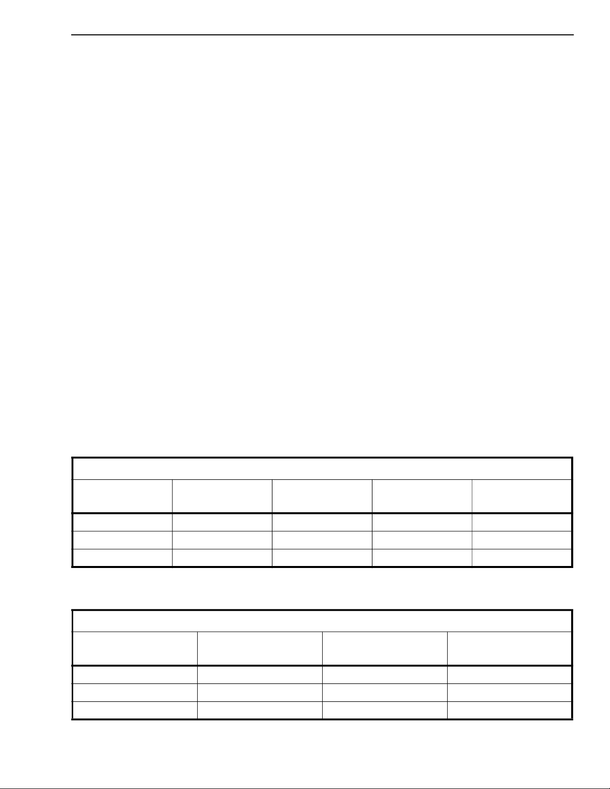
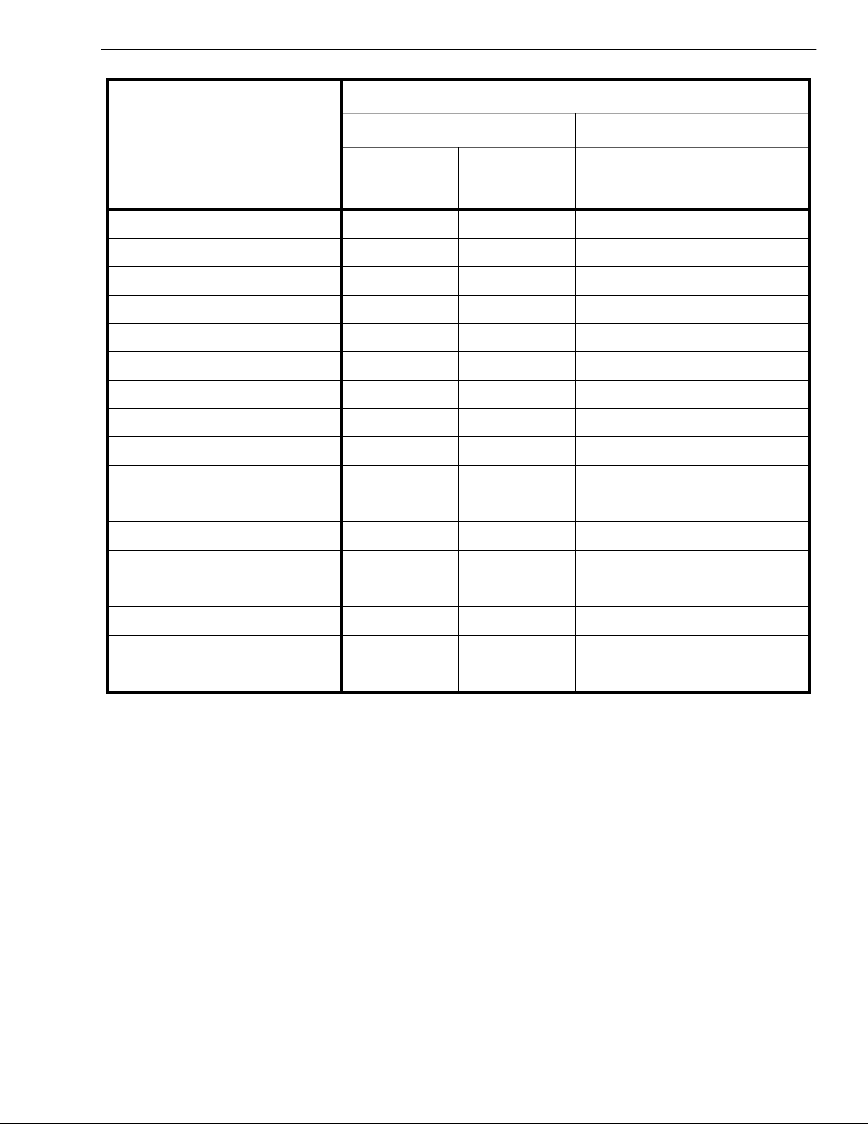
PLL. Tables 6 and 7 show the average measured
intrinsic jitter of the T1 and E1 outputs. Each
measurement is an average based upon a ±100 ppm
deviation (in steps of 20 ppm) on the input reference
clock. Jitter on the master clock will increase intrinsic
jitter of the device, hence attention to minimization of
master clock jitter is required.
Jitter Transfer Function
The jitter transfer function is a measure of the
transfer characteristics of the PLL to frequency
specific jitt er on the refere nced input o f th e PL L. It is
directly linked to the loop bandwidth and the
magnitude of the phase error suppression
characteristics of the P LL. It is measured by applying
jitter of specific magnitude and frequencies to the
input of the PLL, then measuring the magnitude of
the output jitter (both filtered and unfiltered) on the
T1 or E1 output.
Care must be taken when measuring the transfer
characteristics to ensure that critical jitter alias
frequencies are included in the measurement (i.e.,
for digital phase locked loops using an 8 kHz input).
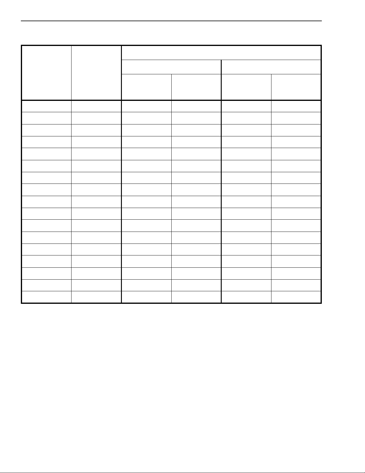
Tables 8 and 9 provide measured results for the jitter
transfer characteristics of the PLL for both a 1.544
MHz and 2.048 MHz reference input clock. The
transfer characteristics for an 8 kHz reference input
will be the same.
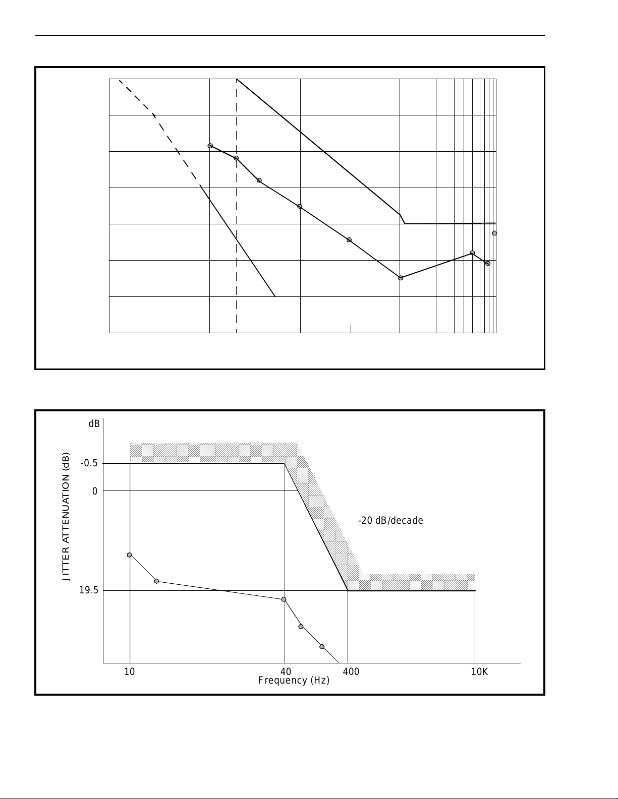
Figures 5 and 6 show the jitter attenuation
performance of the T1 and E1 outputs plotted
against AT & T TR62411 and ETSI requirements,
respectively.
Output Jitter in UIp-p
Reference Input FLT 0 Unfil tered
8 kHz .011 .004 .006 .002
1.544 MHz .011 .001 .002 .001
2.048 MHz .011 .001 .002 .001
Table 6 -Typical Intri nsi c Jitter for the T1 Outpu t
Typical f igures are at 25°C and are for design aid only: not guaranteed and not subject to production testing.
Output Jitter in UIp-p
Reference Input FLT0 Unfiltered
8 kHz .011 .002 .002
1.544 MHz .011 .002 .002
2.048 MHz .011 .002 .002
Table 7 - Typical Intr insic Ji tter for the E1 Outpu t
Typical f igures are at 25°C and are for design aid only: not guaranteed and not subject to production testing.
FLT1
10Hz - 8kHz
FLT1
20Hz - 100kHz
FLT2
10Hz - 40kHz
8kHz - 40kHz
700Hz - 100kHz
FLT3
FLT2
3-103
Page 8
MT9042 Preliminary Information
Measured Jitter Ou tput (UIp -p)
Input Jitter
Modulation
Frequency
(Hz)
10 20 2.42 18.34 2.41 18. 38
20 20 1.62 21.83 1.618 21.84
40 20 .900 26.94 .908 26. 86
100 20 .375 34.54 .376 34.52
330 10 .060 44.44 .060 44.44
500 8 .032 47.96 .032 47.96
1000 7 .015 53.38 .015 53.38
5000 0.8 .003 48.52 .003 48.52
7900 1.044 .003 50.83 .0 03 50.83
7950 1.044 .003 50.83 .0 03 50.83
7980 1.044 .003 50.83 .0 03 50.83
Input Jitter
Magnitude
(UIp-p)
T1 Reference Input E1 Reference Input
Output Jitter
Magnitude
(UIp-p)
Jitter
Attenuation
(dB)
Output Jitter
Magnit ude
(UIp-p)
Attenuation
Jitter
(dB)
7999 1.044 .003 50.83 .0 03 50.83
8001 1.044 .003 50.83 .0 03 50.83
8020 1.044 .003 50.83 .0 03 50.83
8050 1.044 .003 50.83 .0 03 50.83
8100 1.044 .003 50.83 .0 03 50.83
10000 0.4 .003 42.50 .003 42.50
Ta bl e 8 - Typical Jit ter Transfer Function for the T1 Output
Notes
1) For input jitter from 10 kHz to 100 kHz, the jitter attenuation is of such magnitude that intrinsic jitter dominates the output
signal, rendering the jitter transfer function unmeasurable.
2) Typical figures are at 25°C and are for design aid only: not guaranteed and not subject to production testing
.
3-104
Page 9
Preliminary Information MT9042
Measured Jitter Outpu t (UIp-p)
Input Jitter
Modulation
Frequency
(Hz)
Input Jitter
Magnitu de
(UIp-p)
T1 Reference Input E1 Reference I np ut
Output Jitter
Magnitud e
(UIp-p)
Jitter
Attenuation
(dB)
Output Jitter
Magnitude
(UIp-p)
Attenuation
10 1.5 .355 12.52 .3 51 12.62
20 1.5 .186 18.13 .1 85 18.18
40 1.5 .095 23.97 .0 96 23.88
100 1.5 .039 31.70 .039 31.70
200 1.5 .021 37.08 .020 37.50
400 1.5 .012 41.94 .012 41.94
1000 1.5 .006 47.96 .007 46.62
7900* 1.044 .002 54.35 .002 54.35
7950* 1.044 .002 54.35 .002 54.35
7980* 1.044 .002 54.35 .002 54.35
7999* 1.044 .002 54.35 .002 54.35
Jitter
(dB)
8001* 1.044 .002 54.35 .002 54.35
8020* 1.044 .002 54.35 .002 54.35
8050* 1.044 .002 54.35 .002 54.35
8100* 1.044 .002 54.35 .002 54.35
10000 0.3 5 .004 38.84 .003 41.34
100000 0.20 .004 33.98 .003 36.48
Ta ble 9 - Typical Jitter Transfer Function for the E 1 Output
Notes
1) For input jitter from 10 kHz to 100 kHz, the jitter attenuation is of such magnitude that intrinsic jitter dominates the output
signal, rendering the jitter transfer function unmeasurable.
2) Typical figures are at 25°C and are for design aid only: not guarante ed and not subject to production testing
* Output jitter dominated by intrinsic jitter.
.
3-105
Page 10
MT9042 Preliminary Information
AAAA
AAAA
AAAA
AAAA
AAAA
AAAA
AAAA
AAAA
AAAA
AAAA
AAAA
AAAA
AAAA
AAAA
AAAA
AAAA
AAAA
AAAA
AAAA
AAAA
AAAA
AAAA
AAAA
AAAA
AAAA
AAAA
AAAA
AAAA
AAAA
AAAA
AAAA
AAAA
AAAA
AAAA
AAAA
AAAA
AAAA
AAAA
AAAA
AAAA
AAAA
AAAA
AAAA
AAAA
AAAA
AAAA
AAAA
AAAA
AAAA
AAAA
AAAA
AAAA
AAAA
AAAA
AAAA
AAAA
AAAA
AAAA
AAAA
AAAA
AAAA
AAAA
AAAA
AAAA
AAAA
AAAA
AAAA
AAAA
AAAA
AAAA
AAAA
AAAA
AAAA
AAAA
AAAA
AAAA
AAAA
AAAA
AAAA
AAAA
AAAA
AAAA
AAAA
AAAA
AAAA
AAAA
AAAA
AAAA
AAAA
AAAA
AAAA
AAAA
AAAA
AAAA
AAAA
AAAA
AAAA
AAAA
AAAA
AAAA
AAAA
AAAA
AAAA
AAAA
AAAA
AAAA
AAAA
AAAA
AAAA
AAAA
AAAA
AAAA
AAAA
AAAA
AAAA
AAAA
AAAA
AAAA
AAAA
AAAA
AAAA
AAAA
AAAA
AAAA
AAAA
AAAA
AAAA
AAAA
AAAA
AAAA
AAAA
AAAA
AAAA
AAAA
AAAA
AAAA
AAAA
AAAA
AAAA
AAAA
AAAA
AAAA
AAAA
AAAA
AAAA
AAAA
AAAA
AAAA
AAAA
AAAA
AAAA
AAAA
AAAA
AAAA
AAAA
AAAA
AAAA
AAAA
AAAA
AAAA
AAAA
AAAA
AAAA
AAAA
AAAA
AAAA
AAAA
AAAA
AAAA
AAAA
AAAA
AAAA
AAAA
AAAA
AAAA
AAAA
AAAA
AAAA
AAAA
AAAA
AAAA
AAAA
AAAA
AAAA
AAAA
AAAA
AAAA
AAAA
AAAA
AAAA
AAAA
AAAA
AAAA
AAAA
AAAA
AAAA
AAAA
AAAA
AAAA
AAAA
AAAA
AAAA
AAAA
AAAA
AAAA
AAAA
AAAA
AAAA
AAAA
AAAA
AAAA
AAAA
AAAA
AAAA
AAAA
AAAA
AAAA
AAAA
AAAA
AAAA
AAAA
AAAA
AAAA
AAAA
AAAA
AAAA
AAAA
AAAA
AAAA
AAAA
AAAA
AAAA
AAAA
AAAA
AAAA
AAAA
AAAA
AAAA
AAAA
AAAA
AAAA
AAAA
AAAA
AAAA
AAAA
AAAA
AAAA
AAAA
AAAA
AAAA
AAAA
AAAA
AAAA
AAAA
AAAA
AAAA
AAAA
AAAA
AAAA
AAAA
AAAA
AAAA
AAAA
AAAA
AAAA
AAAA
AAAA
AAAA
AAAA
AAAA
AAAA
AAAA
AAAA
AAAA
AAAA
AAAA
AAAA
AAAA
AAAA
AAAA
AAAA
AAAA
AAAA
AAAA
AAAA
AAAA
AAAA
AAAA
AAAA
AAAA
AAAA
AAAA
AAAA
AAAA
AAAA
AAAA
AAAA
AAAA
AAAA
AAAA
AAAA
AAAA
AAAA
AAAA
AAAA
AAAA
AAAA
AAAA
AAAA
AAAA
AAAA
AAAA
AAAA
AAAA
AAAA
AAAA
AAAA
AAAA
AAAA
AAAA
AAAA
AAAA
AAAA
AAAA
AAAA
AAAA
AAAA
AAAA
AAAA
AAAA
AAAA
AAAA
AAAA
AAAA
AAAA
AAAA
AAAA
AAAA
AAAA
AAAA
AAAA
AAAA
AAAA
AAAA
AAAA
AAAA
AAAA
AAAA
AAAA
AAAA
AAAA
AAAA
AAAA
AAAA
AAAA
AAAA
AAAA
AAAA
AAAA
AAAA
AAAA
AAAA
AAAA
AAAA
AAAA
AAAA
AAAA
AAAA
AAAA
AAAA
AAAA
AAAA
AAAA
AAAA
AAAA
AAAA
AAAA
AAAA
AAAA
AAAA
AAAA
AAAA
AAAA
AAAA
AAAA
AAAA
AAAA
AAAA
AAAA
AAAA
AAAA
AAAA
AAAA
AAAA
AAAA
AAAA
AAAA
AAAA
AAAA
AAAA
AAAA
AAAA
AAAA
AAAA
AAAA
AAAA
AAAA
AAAA
AAAA
AAAA
AAAA
AAAA
AAAA
AAAA
AAAA
AAAA
AAAA
AAAA
AAAA
AAAA
AAAA
AAAA
AAAA
AAAA
AAAA
AAAA
AAAA
AAAA
AAAA
AAAA
AAAA
AAAA
AAAA
AAAA
AAAA
AAAA
AAAA
AAAA
AAAA
AAAA
AAAA
AAAA
AAAA
AAAA
AAAA
AAAA
AAAA
AAAA
AAAA
AAAA
AAAA
AAAA
AAAA
AAAA
AAAA
AAAA
AAAA
AAAA
AAAA
AAAA
AAAA
AAAA
AAAA
AAAA
AAAA
AAAA
AAAA
AAAA
AAAA
AAAA
AAAA
AAAA
AAAA
AAAA
AAAA
AAAA
AAAA
AAAA
AAAA
AAAA
AAAA
AAAA
AAAA
AAAA
AAAA
AAAA
AAAA
AAAA
AAAA
AAAA
AAAA
AAAA
AAAA
AAAA
AAAA
AAAA
AAAA
AAAA
AAAA
AAAA
AAAA
AAAA
AAAA
AAAA
AAAA
AAAA
AAAA
AAAA
AAAA
AAAA
AAAA
AAAA
AAAA
AAAA
AAAA
AAAA
AAAA
AAAA
AAAA
AAAA
AAAA
AAAA
AAAA
AAAA
AAAA
AAAA
AAAA
AAAA
AAAA
AAAA
AAAA
AAAA
AAAA
AAAA
AAAA
AAAA
AAAA
AAAA
AAAA
AAAA
AAAA
AAAA
AAAA
AAAA
AAAA
AAAA
AAAA
AAAA
AAAA
AAAA
AAAA
AAAA
AAAA
AAAA
AAAA
AAAA
AAAA
AAAA
AAAA
AAAA
AAAA
AAAA
AAAA
AAAA
AAAA
AAAA
AAAA
AAAA
AAAA
AAAA
AAAA
AAAA
AAAA
AAAA
AAAA
AAAA
AAAA
AAAA
AAAA
AAAA
AAAA
AAAA
AAAA
AAAA
AAAA
AAAA
AAAA
AAAA
AAAA
AAAA
AAAA
AAAA
AAAA
AAAA
AAAA
AAAA
AAAA
AAAA
AAAA
AAAA
AAAA
AAAA
AAAA
AAAA
AAAA
AAAA
AAAA
AAAA
AAAA
AAAA
AAAA
AAAA
AAAA
AAAA
AAAA
AAAA
AAAA
AAAA
AAAA
AAAA
AAAA
AAAA
AAAA
AAAA
AAAA
AAAA
AAAA
AAAA
AAAA
AAAA
AAAA
AAAA
AAAA
AAAA
AAAA
AAAA
AAAA
AAAA
AAAA
AAAA
AAAA
AAAA
AAAA
AAAA
AAAA
AAAA
AAAA
AAAA
AAAA
AAAA
AAAA
AAAA
AAAA
AAAA
AAAA
AAAA
AAAA
AAAA
AAAA
AAAA
AAAA
AAAA
AAAA
AAAA
AAAA
AAAA
AAAA
AAAA
AAAA
AAAA
AAAA
AAAA
AAAA
AAAA
AAAA
AAAA
AAAA
AAAA
AAAA
AAAA
AAAA
AAAA
AAAA
AAAA
AAAA
AAAA
AAAA
AAAA
AAAA
AAAA
AAAA
AAAA
AAAA
AAAA
AAAA
AAAA
AAAA
AAAA
AAAA
AAAA
AAAA
AAAA
AAAA
AAAA
AAAA
AAAA
AAAA
AAAA
AAAA
AAAA
AAAA
AAAA
AAAA
AAAA
AAAA
AAAA
AAAA
AAAA
AAAA
AAAA
AAAA
AAAA
AAAA
AAAA
AAAA
AAAA
AAAA
AAAA
AAAA
AAAA
AAAA
AAAA
AAAA
AAAA
AAAA
AAAA
AAAA
AAAA
AAAA
AAAA
AAAA
AAAA
AAAA
AAAA
AAAA
AAAA
AAAA
AAAA
AAAA
AAAA
AAAA
AAAA
AAAA
AAAA
AAAA
AAAA
AAAA
AAAA
AAAA
AAAA
AAAA
AAAA
AAAA
AAAA
AAAA
AAAA
AAAA
AAAA
AAAA
AAAA
AAAA
AAAA
AAAA
AAAA
AAAA
AAAA
AAAA
AAAA
AAAA
AAAA
AAAA
AAAA
AAAA
AAAA
AAAA
AAAA
AAAA
AAAA
AAAA
AAAA
AAAA
AAAA
AAAA
AAAA
AAAA
AAAA
AAAA
AAAA
AAA
AAA
AAA
AAA
AAA
AAA
AAA
AAA
AAA
AAA
AAA
AAA
AAA
AAA
AAA
AAA
AAA
AAA
AAA
AAA
AAA
AAA
AAA
AAA
AAA
AAA
AAA
AAA
AAA
AAA
AAA
AAA
AAA
AAA
AAA
AAA
AAA
AAA
0
b) a)
10
SLOPE -20 dB PER DECADE
20
30
SLOPE -40 dB
40
50
JITTER ATTENUATION (dB)
60
PER DECADE
JITTER ATTENUATION (dB)
1 10 20 100 300 1K 10K
Frequency (Hz)
Figure 5 - Typical Jitter Attenuati on for T1 Outp ut
dB
-0.5
0
-20 dB/decade
19.5
3-106
10 40 400 10K
Figure 6 - Typical Jitter Attenuation for E1 Output
Frequency (Hz)
Page 11
Preliminary Information MT9042
Absolute Maximum Ratings*- Voltages are with respect to ground (V
) unless otherwise stated.
SS
Parameter Symbol Min Max Units
1 Supply Voltage V
2 Voltage on any pin V
3 Input/Output Diode Current I
4 Output Source or Sink Current I
5 DC Supply or Ground Current I
6 Storage Temp erature T
7 Package Power Dissipatio n PLCC P
* Exceeding these values may cause perm an ent dama ge. Functi onal operati on under these cond ition s is not implied.
DD
I
IK/OK
O
DD/ISS
ST
D
Recommended Operating Cond itions - Vo ltages are with respect to ground (V
Characteristics Sym Min Typ
1 Su pply Voltage V
2 Inp ut HIGH Voltage V
3 Input LOW Voltage V
4 Operating Temperature T
‡ Typical figures are at 25°C and are for design aid only: not guaranteed and not subject to producti on testing.
DD
IH
IL
A
4.5 5.0 5.5 V
2.0 V
V
SS
-40 25 85 °C
‡
Max Units Test Conditio ns
DD
0.8 V
-0.3 7.0 V
VSS-0.3 VDD+0.3 V
-55 125 °C
) unless otherwise stated.
SS
V
±150 mA
±150 mA
±300 mA
900 mW
DC Electrical Characteristics - Voltages are with respect to gro un d (V
V
=5.0 V±10%; V
DD
=0V; TA =-40 to 85°C.
SS
) unless otherwise stated.
SS
Characteristics Sym Min Typ‡Max Units Test Conditions
S
U
1
2
3 Input LOW voltage V
4
5 Output current LOW I
Supply Current
P
Input HIGH voltage V
I
N
O
Output current HIGH I
U
T
6 Leakage curren t on all inputs I
‡ Typical figures are at 25°C and are for design aid only: not guaranteed and not subject to producti on testing.
I
DD
OH
OL
IL
2.0 V
IH
IL
-4 mA VOH=2.4 V
4mAV
55 mA Under operating condition
0.8 V
10 µA
VIN=V
=0.4 V
OL
SS
3-107
Page 12
MT9042 Preliminary Information
†
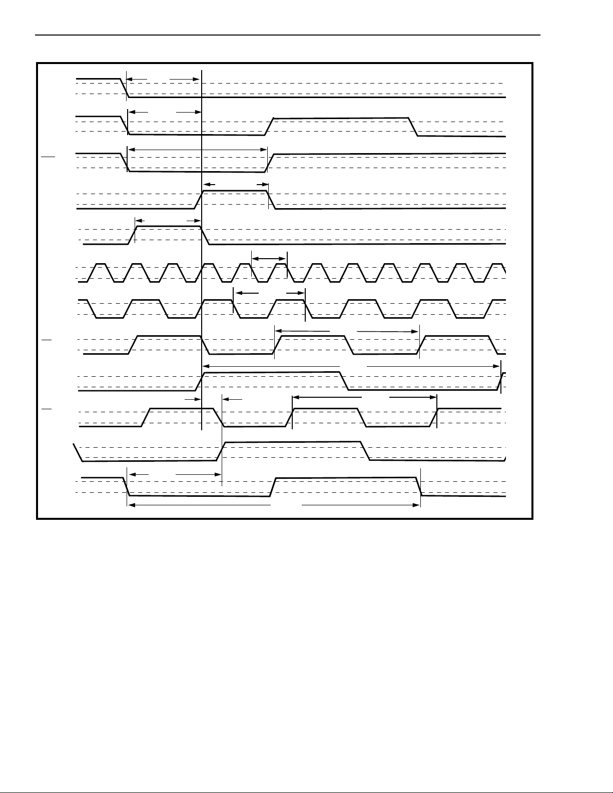
AC Electrical Characteristics (see Fig. 7)
Characteristics Sym Min Typ‡Max Units Test Conditions
-Voltages are with respect to ground (V
) unless otherwise stated.
SS
1 8 kHz reference clock period t
2
1.544 MHz reference clock period t
3 2.048 MHz reference clock period t
I
4 Input to output propagation delay
N
with an 8 kHz reference clock
P
5 Input to output propagation delay
U
with a 1.544 MHz reference clock
T
S
6 Input to output propagation delay
with a 2.048 MHz reference clock
7 Input rise time (except MCLKi and
GTi)
8 Input fall time (except MCLKi and
GTi)
9 Delay between C1.5 and C2 t
10 Frame pulse F0o
output pulse
width
11 Frame pulse F0o
12 Frame pulse F0o
13 Frame pulse FP8-STB output
pulse width
output rise time t
output fall time t
t
P8R
P15R
P20R
t
PD8
t
PD15
t
PD20
D-20-15
t
W-F0o
R-F0o
F-F0o
W-FP8STB
125 µs
648 ns
488 ns
183 ns
243 ns
183 ns
MCLKi =
20.000 000MHz
MCLKi =
20.000 000MHz
MCLKi =
20.000 000MHz
8ns
8ns
18 ns
244 ns
5 9 ns Load = 85pF
5 9 ns Load = 85pF
122 ns
14 Frame pulse FP8-STB output rise
time
15 Frame pulse FP8-STB output fall
time
16 O
17 Frame pulse FP8-GCI output rise
18 Frame pulse FP8-GCI outp ut fall
Frame pulse FP8-GCI output
U
pulse width
T
P
time
U
T
S
time
19 C1.5 clock period t
20 C1.5 clock output rise time t
21 C1.5 clock output fall time t
t
R-FP8STB
t
F-FP8STB
t
W-FP8GCI
t
R-FP8GCI
t
F-FP8GC
P-C1.5
RC1.5
FC1.5
59ns
59ns
122 ns
59ns
I
59ns
648 ns
5 9 ns Load = 85pF
5 9 ns Load = 85pF
22 C1.5 clock output duty cycle 50 %
23 C3
24 C3
25 C3
26 C3
clock period t
clock output rise t im e t
clock output fall tim e t
P-C3
RC3
FC3
324 ns
5 9 ns Load = 85pF
5 9 ns Load = 85pF
clock output duty cycle 50 %
Load = 85pF
Load = 85pF
Load = 85pF
Load = 85pF
27 C2 clock period t
28 C2 clock output rise time t
3-108
P-C2
RC2
488 ns
5 9 ns Load = 85pF
Page 13
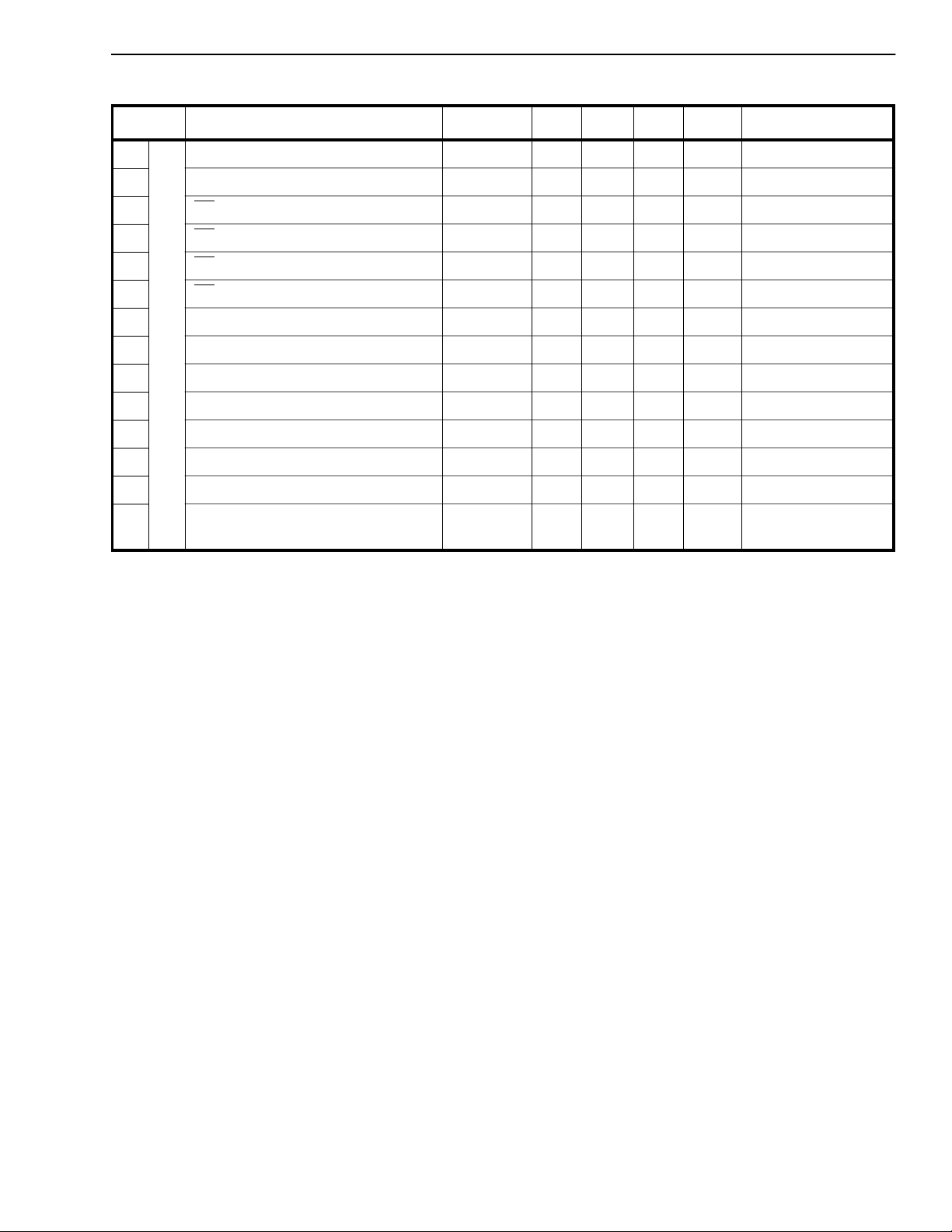
Preliminary Information MT9042
†
AC Electrical Characteristics (see Fig. 7)
Characteristics Sym Min Typ‡Max Units Test Conditions
-Voltages are with respect to ground (V
) unless otherwise stated.
SS
29 C2 clock output fall time t
FC2
5 9 ns Load = 85pF
30 C2 clock output duty cycle 50 %
31 C4
32 C4
33 C4
34 O
U
35 C8 clock period t
T
P
36 C8 clock output rise time t
U
37 C8 clock output fall time t
T
S
38 C8 clock output duty cycle 50 %
39 C16 clock period t
40 C16 clock output rise time t
41 C16 clock output fall time t
42 C16 clock output duty cycle
†
-Timing is over recommended temperature & power supply voltages.
‡
-Typical figures are at 25°C and are for design aid only: not guaranteed and not subject to production testing.
clock period t
clock output rise time t
clock output fall time t
C4
clock output duty cycle 50 %
P-C4
RC4
FC4
P-C8
RC8
FC8
P-C16
RC16
FC16
244 ns
5 9 ns Load = 85pF
5 9 ns Load = 85pF
122 ns
5 9 ns Load = 85pF
5 9 ns Load = 85pF
61 ns
5 9 ns Load = 85pF
5 9 ns Load = 85pF
43 50 55 %
Duty cycle on
MCLKi =50%
3-109
Page 14
MT9042 Preliminary Information
t
PD-8
PRI- 8 kHz
t
PD-20
PRI-2.048 MHz
t
W-F0o
F0o
t
W-FP8STB
FP8-STB
t
W-FP8GCI
FP8-GCI
t
P-C16
C16
t
P-C8
C8
C4
C2
C3
C1.5
PRI-1.544 MHz
t
PD-15
t
P-C4
t
P-C2
t
t
D-20-15
t
P-C1.5
P-C3
Figure 7 - Timing Inform ati on for MT 90 42
3-110
Page 15
Preliminary Information MT9042
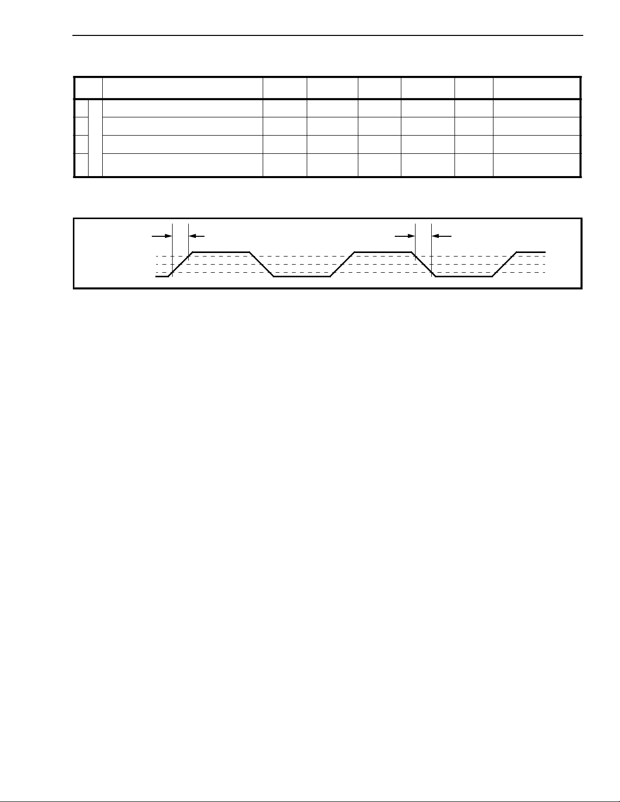
AC Electrical Characteristics (see Fig . 8)† - Voltages are with respect to ground (V
Characteristics Sym Min Typ
1C
Master clock input rise time t
L
2 Master clock input fall time t
O
C
3 Master clo ck frequency t
K
4 Duty Cycle of the master clock
† Timing is over recommended temperature & power supply voltages
‡ Typical figures are at 25°C and are for design aid only: not guaranteed and not subject to producti on testing
t
rMCLK
MCLKi
2.4V
1.5V
0.4V
rMCLKi
fMCLKi
pMCLKi
19.99936 20 20.000640 MHz
40 50 60 %
‡
Max Units Test Conditions
4ns
4ns
SS
t
Figure 8 - Master Clock Input
) unless otherwise stated.
fMCLK
3-111
Page 16

MT9042 Preliminary Information
Notes:
3-112
 Loading...