

Page 1
AAAA
AAAA
AAAA
AAAA
A
A
A
A
A
A
A
A
A
A
AA
AAAA
AAAA
AAAA
AAAA
AAAA
A
A
A
A
A
A
A
A
A
A
2
ISO
-CMOS ST-BUS FAMILY
MT9092
Digital Telephone with HDLC (HPhone-II)
Features
• Programmable µ-Law/A-Law codec and filters
• Program mable CCITT (G .711)/sign-magni tude
coding
• Program mab le trans mit , receiv e and si de-t one
gains
• DSP-based:
i) Speakerphone switching algorithm
ii) DTMF and single tone generator
iii) Tone Ringer
• Differential interf ace to telepho ny tra nsdu cers
• Differential audio paths
• Singl e 5 volt pow er su ppl y
• X.25 Level 2 HD LC data form at ting
Applications
• Fully f eatu red dig ital t eleph one set s
• Cellula r phone sets
• Local area com m unications stations
ISSUE 2 May 1995
Ordering Information
MT9092AP 44 Pin PLCC
-40°C to +85°C
Description
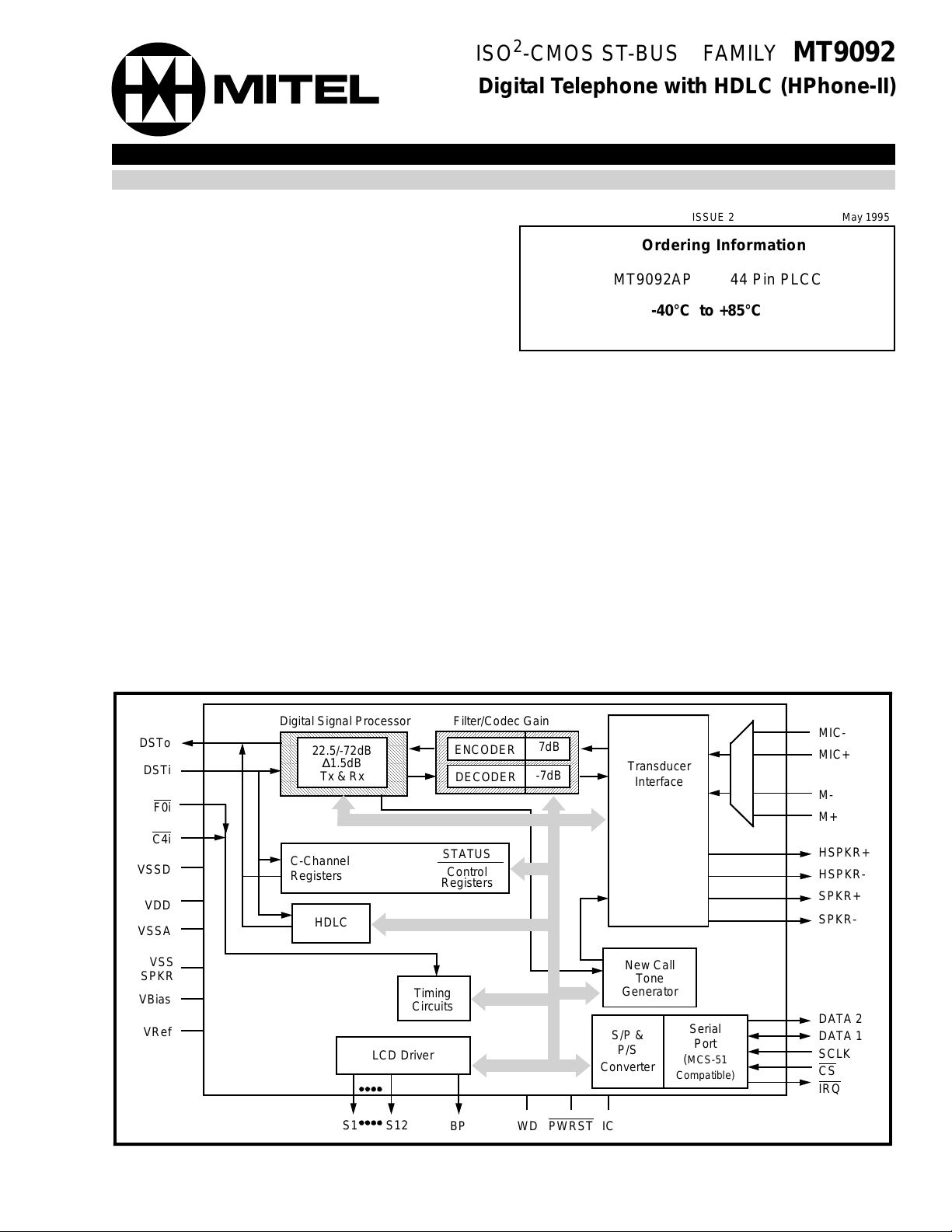
The MT9092 HPhone-II is a fully featured integrated
digital telephone circuit which includes an HDLC
data formatter. Voice band signals are converted to
digital PCM and vice versa by a switched capacitor
Filter/Codec. The Filter/Codec uses an ingenious
differential architecture to achieve low noise
operation over a wide dynamic range with a single
5V supply. A Digital Signal Processor provides
handsfree speaker-phone operation. The DSP is
also used to generate tones (DTMF, Ringer and Call
Progress) and control audio gains. Internal registers
are accessed through a serial microport conforming
to INTEL MCS-51™ specifications. The device is
fabricated in Mitel's low power ISO
technology.
2
-CMOS
DSTo
DSTi
F0i
C4i
VSSD
VDD
VSSA
VSS
SPKR
VBias
VRef
Digital Signal Processor Filter/Codec Gain
AAA
AAAA
AAAA
AAAA
AAAA
A
AAA
AAAA
AAAA
AAAA
AAA
AAAA
AAA
AAAA
22.5/-72dB
AAA
AAAA
AAA
AAAA
∆1.5dB
AAA
AAAA
AAA
AAAA
Tx & Rx
AAA
AAAA
AAA
AAAA
AAA
AAAA
C-Channel
Registers
AAAA
AAAA
AAAA
AAAA
AAAA
AAAA
AAAA
AAAA
AAAA
AAAA
AAAA
AAAA
AAAA
AAAA
AAAA
AAAA
AAAA
AAAA
AAAA
AAAA
AAAA
AAAA
AAAA
AAAA
AAAA
AAAA
AAAA
A
AAA
AAAA
AAA
AAAA
ENCODER
AAA
AAAA
AAA
AAAA
AAA
AAAA
AAA
AAAA
DECODER
AAA
AAAA
AAA
AAAA
AAA
AAAA
AAAA
AAAA
AAAA
AAAA
AAAA
AAAA
AAAA
AAAA
AAAA
A
A
A
A
A
A
A
A
STATUS
Control
Registers
AAAA
AAAA
AAAA
AAAA
AAAA
AAAA
AAAA
AAAA
AAAA
AAAA
AAAA
AAAA
AAAA
AAAA
AAAA
AAAA
-7dB
AAAA
AAAA
AAAA
HDLC
Timing
Circuits
LCD Driver
S1 S12
BP WD PWRST
Figure 1 - Functional Block Diagram
7dB
AAAA
AAAA
AAAA
AAAA
AAAA
AAAA
AAAA
AAAA
AAAA
AAAA
Transd ucer
Interface
New Call
Tone
Generator
S/P &
P/S
Converter
IC
Serial
Port
MCS-51
(
Compatible)
MICMIC+
MM+
HSPKR+
HSPKRSPKR+
SPKR-
DATA 2
DATA 1
SCLK
CS
IRQ
7-3
Page 2
MT9092
PWRST
IC
VBias
VRef
NCM-VSSA
M+
MIC+
MIC-
VSS SPKR
VSSD
1
4443424140
23
2425262728
S1
S3S4S5S6S7
S2
39
38
37
36
35
34
33
32
31
30
29
SPKR+
SPKRHSPKR+
HSPKRVDD
BP
S12
S11
S10
S9
S8
DSTi
DSTo
C4i
F0i
VSSD
IRQ
SCLK
DATA 2
DATA 1
CS
WD
65432
7
8
9
10
11
12
13
14
15
16
17
1819202122
IC
NC
NC
44 PIN PLCC
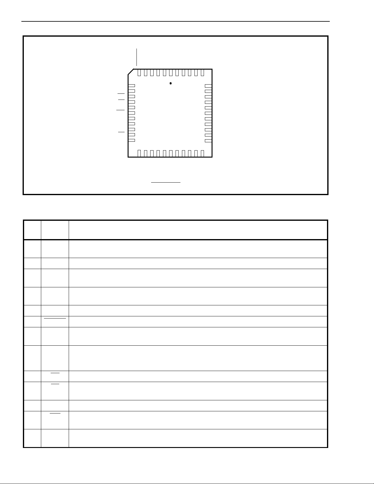
Figure 2 - Pin Connections
Pin Description
Pin
Name Description
#
1M+Non-Inver tin g Micro ph one (Input). Non-inverti ng input to microphone am plif ier from the
handset microphone.
2NCNo Connect. No internal connecti on to this pin.
3V
Bias
4V
5ICInternal Connection. Tie externally to V
6 PWRST
Bias Voltage (Outpu t). (VDD/2) volts is available at this pin for biasing external ampli fier s.
Connect 0.1 µF capacitor to V
Reference voltage for codec (Output). Nominally [(VDD/2)-1.5] volts. Used internally.
Ref
Connect 0.1 µF capacit or to V
SSA
SSA
.
.
for normal operation.
SS
Power-up Reset (Input). CMOS compatible input with Schmit t Trigger (active low).
7DSTiST-BUS Serial Stream (Input). 2048 kbit/s input stream composed of 32 eight bit channels;
the first four of which are used by the MT9092. Input level is TTL compat ibl e.
8DSToST-BUS Serial Stream (Output). 2048 kbit/s output stream composed of 32 eight bit
channels. The MT9092 sources digital signals during the appropriate channel, time coincident
with the channels used for DSTi.
9C4i
10 F0i
4096 kHz Clock (Input). CMOS level compatible.
Frame Pul se (Inp ut ). CMOS level compatible. This input is the frame synchronization pulse
for the 2048 kbit/ s ST-BUS stream.
11 V
SSD
12 IRQ
Digital Ground . Nominally 0 volts.
Interrupt Request (Open Drain Output). An active low output indicating an unmasked HDLC
interrupt event. Req uires 1 kΩ pull-up to V
DD
.
13 SCLK Serial Po rt Syn chro no us Cl ock (In pu t). Data clock for MCS-51 compa tibl e micropo rt. TTL
level compatible.
7-4
Page 3

Pin Description (continued)
MT9092
Pin
Name Description
#
14 DATA 2 Serial Data Transmit. In an alternate mode of operation, this pin is used for data transmit
from MT9092. In the default mode, serial data transmi t and receive are performed on the
DATA 1 pin and DATA 2 is tri-stated.
15 DATA 1 Bidirectional Serial Data. Port for microprocessor serial data transfer compatible wit h MCS-
51 standard (default mode). In an alternat e mode of operati on , this pin becomes the data
receive pin only and data transmit is performed on the DATA 2 pin. Input level TTL compatible.
16 CS
Chip Select (Input). This input signal is used to select the device for microport data
transfers. Active low. (TTL level compatible .)
17 WD Watchdog (Output). Watchdog timer output. Active high.
18 IC Internal Connection. Tie externally to V
19,
NC No Connection. No internal connection to these pins.
for normal operation.
SS
20
21 V
SSD
Digital Ground. Nominall y 0 volt s.
22-33S1-S12 Segment Drivers (Output). 12 independently controlled, two level, LCD segment drivers. An
in-phase signal, with respect to the BP pin, produces a non-energized LCD segment . An out-
of-phase signal, with respect to the BP pin, energizes its respective LCD segment.
34 BP Backplane Drive (Output). A two-level output voltag e for biasing an LCD backplane.
35 V
Positive Po wer Supply (Inp ut). Nominally 5 volt s .
DD
36 HSPKR- I nvertin g Hand set Speaker (Outpu t). Output to the handset speaker (balanced).
37 HSPKR+Non-Inver tin g Handset Sp eaker (Outp ut). Output to the handset speaker (balanced).
38 SPKR- Inverting Speake r (Outpu t). Output to the speakerphone speaker (balanced).
39 SPKR+ Non-Inverting Speaker (Outpu t). Output to the speakerphone speaker (balanced).
40 V
Power Supply Rail for Analog Output Drivers. N o min ally 0 Volts.
SS
SPK R
41 MIC- Inve rtin g Handsfree M icr oph on e (Inp ut). Handsfree microphone amplif ier invert ing input
pin.
42 MIC+ No n-inver tin g Hand sfree Micro ph on e (Inp ut). Handsfree microphone amplifier non-
inverting input pin.
43 V
SSA
Anal og G round. Nominall y 0 V.
44 M- Inve rtin g Micro ph on e (Inp ut). Inverting input to microphone am plif ier from the handse t
microphone.
NOTES:
Intel and MCS-51 are registered trademarks of Intel Corporation, Santa Clara, CA, USA.
7-5
Page 4

MT9092
Overview
The functional block diagram of Figure 1 depicts the
main operations performed within the HPhone-II.
Each of these functional blocks will be described in
the sections to follow. This overview will describe
some of the end-user features which may be
implemented as a direct result of the level of
integration found within the HPhone-II.
The main feature required of a digital telephone is to
convert the digital Pulse Code Modulated (PCM)
information, be ing rece ived by the telephon e set, into
an analog electrical signal. This signal is then
applied to an appropriate audio transducer such that
the information is finally converted into intelligible
acoustic energy. The same is true of the reverse
direction where acoustic energy is converted first
into an electrical analog and then digitized (into
PCM) before being transmitted from the set. Along
the way if the signals can be manipulated, either in
the analog or the digital domains, other features
such as gain control, signal generation and filtering
may be added. More complex processing of the
digital signal is also possible and is limited only be
the processing power available. One example of this
processing power may be the inclusion of a complex
handsfree switching algorithm. Finally, most electroacoustic transducers (loudspeakers) require a large
amount of power to develop an effective acoustic
signal. The inclusion of audio amplifiers to provide
this power is required.
The HPhone-II features Digital Signal Processing
(DSP) of the voice encoded PCM, complete Analog/
Digital and Digital/Analog conversion of audio
signals (Filter/CODEC) and an analog interface to
the external world of electro-acoustic devices
(T ransducer Interface). These three functional blocks
combine to provide a standard full-duplex telephone
conversation utilizing a common handset. Selecting
transducers for handsfree operation, as well as
allowing the DSP to perform its handsfree switching
algorithm, is all that is required to convert the fullduplex handset conversation into a half-duplex
speakerphone conversation. In each of these
modes, full programmability of the receive path and
side-tone gains is available to set comfortable
listening levels for the user as well as transmit path
gain control for setting nominal transmit levels into
the network.
The ability to generate tones locally provides the
designer with a familiar method of feedback to the
telephone user as they proceed to set-up, and
ultimately, dismantle a telephone conversation. Also,
as the network slowly evolves from the dial pulse/
DTMF methods to the D-Channel protocols it is
essential that the older methods be available for
backward compatibility. As an example; once a call
has been established, say from your office to your
home, using the D-Channel signalling protocol it may
be necessary to use in-band DTMF signalling to
manipulate your personal answering machine in
order to retrieve messages. Thus the locally
generated tones must be of network quality and not
just a reasonable facsimile. The HPhone-II DSP can
generate the required tone pairs as well as single
tones to accommodate any in-band signalling
requirement.
Each of the programmable parameters within the
functional blocks is accessed through a serial
microcontroller port compatible with Intel MCS-51
specifications.
Functional Descripti on
In this section, each functional block within the
HPhone-II is described along with all of the
associated control/status bits. Each time a control/
status bit(s) is described it is followed by the address
register where it will be found. T he reader is r eferred
to the section titled ‘Register Summary' for a
complete listing of all address map registers, the
control/status bits associated with each register and
a definition of the function of each control/status bit.
The Register Summary is useful for future reference
of control/status bits without the need to locate them
within th e tex t o f th e f unctional des crip ti o ns.
Filter-CODEC
The Filter/CODEC block implements conversion of
the analog 3.3kHz speech signals to/from the digital
domain compatible with 64kb/s PCM B-Channels.
Selection of companding curves and digital code
assignment are register programmable. These are
CCITT G.711 A-law or µ-Law, with true-sign/
Alternate Digit Inversion or true-sign/Inverted
Magnitude coding, respectively. Optionally, signmagnitude coding may also be selected for
proprietary applications.
The HPhone-II’s HDLC block is easy to use in
proprietary signalling protocols such as those within
PABXs and Key Systems. A fully interrupt driven
interface, buffered by 19 byte FIFOs in each
direction, simplifies the microcontroller's
asynchronous ac cess to the D-Cha n nel in fo rm at ion.
7-6
The Filter/CODEC block also implements transmit
and receive audio path gains in the analog domain.
These gains are in addition to the digital gain pad
provided in the DSP section and provide an overall
path gain resolution of 0.5dB. A programmable gain,
Page 5
MT9092
voice side-tone path is also included to provide
proportional transmit speech feedback to the
handset receiver so that a dead sounding handset is
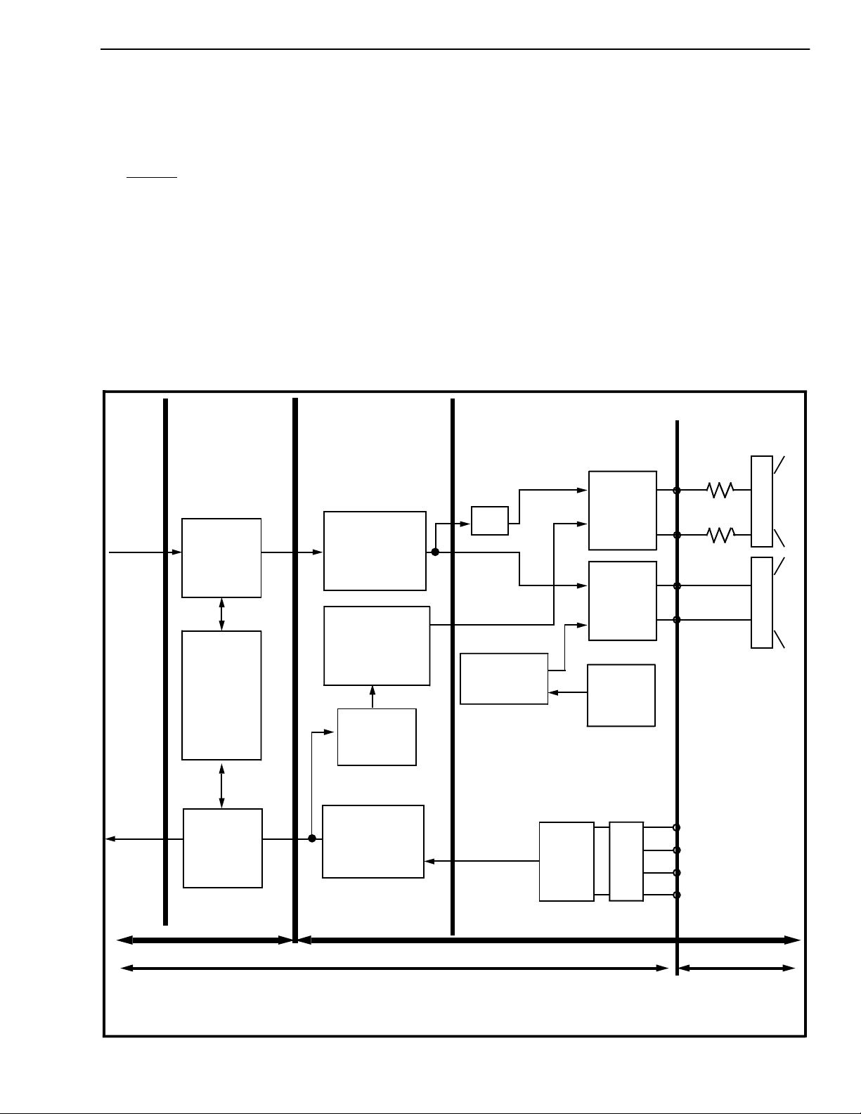
not encountered. Figure 3 depicts the nominal halfchannel and side-tone gains for the HPhone-II.
On PWRS T
(pin 6) the Filter/CODEC defaults such
that the side-tone path, dial tone filter and 400Hz
transmit filter are off, all programmable gains are set
to 0dB and µ-Law companding is selected. Further,
the Filter/CODEC is powered down due to the PuFC
bit (Transducer Control Register, address 0Eh) being
reset. This bit must be set high to enable the Filter/
CODEC.
The internal architecture is fully differential to provide
the best possible noise rejection as well as to allow a
SERIAL
PORT
DSP GAIN*
FILTER/CODEC
wide dynamic range from a single 5 volt supply
design. This fully differential architecture is
continued into the Transducer Interface section to
provide full chip realization of these capabilites.
A reference voltage (V
), for the conversion
Ref
requirements of the CODER section, and a bias
voltage (V
sections, are both generated on-chip. V
), for biasing the internal analog
Bias
Bias
is also
brought to an external pin so that it may be used for
biasing any external gain plan setting amplifiers. A
0.1µF capacitor must be connected from V
analog ground at all times. Likewise, although V
Bias
to
Ref
may only be used internally, a 0.1µF capacitor from
the V
pin to ground is required at all times. It is
Ref
suggested that the analog ground reference point for
these two cap ac ito r s b e ph y si cal ly the same p o int.
TRANSDUCER INTERFACE
µ-Law –6.3 dB
Α-Law –3.7 dB
-6 dB
HSPKR+
Handset
Receiver
(150Ω)
PCM
PCM
Receive
–72 to
+22.5 dB
(1.5dB
steps)
DTMF,
Tone
Ringer &
Handsfree
–72 to
+22.5 dB
(1.5dB
steps)
Transmit
Receive
Filter Gain
0 to –7 dB
(1 dB steps)
Side-tone
–9.96 to
+9.96d B
(3.32 dB steps)
Side-tone
Nominal
Gain
µ-Law –11 dB
Α-Law –18.8 dB
Transmit
Filter Gain
0 to +7dB
(1 dB steps)
-6 dB
Speaker Gain
0 to –24 dB
(8 dB steps)
µ-Law 6.1dB
Α-Law 15.4dB
Transmit
Gain
Receiver
Driver
Speaker
Phone
Driver
0.2dB*
Tone
Ringer
(input
from DSP)
M
U
X
HSPKR–
SPKR+
SPKR–
MIC+
MIC–
M+
M–
75
75
Speakerphone
Speaker
(40Ω nominal)
(32Ω min)
Handsfree
mic
Transmitter
microphone
DIGITAL DOMAIN
Internal to Device External to Device
Note: *gain the same for A-Law and µ−Law
ANALOG DOMAIN
Figure 3 - Audio Gain Partitioning
7-7
Page 6

MT9092
To facili tate this the V
Ref
and V
pins are situated
Bias
on adjacent pins.
The transmit filter is designed to meet CCITT G.714
specifications. The nominal gain for this filter path is
0dB (gain control = 0dB). An anti-aliasing filter is
included. This is a second order lowpass
implementation with a corner frequency at 25kHz.
Attenuation is better than 32dB at 256 kHz and less
than 0.01dB within the passband.
An optional 400Hz high-pass function may be
included into the transmit path by enabling the Tfhp
bit in the Transducer Control Register (address 0Eh).
This option allows the reduction of transmitted
background noise such as motor and fan noise.
The receive filter is designed to meet CCITT G.714
specifications. The nominal gain for this filter path is
0 dB (gain control = 0dB). Filter response is peaked
to compensate for the sinx/x attenuation caused by
the 8 kH z sam p li ng rat e.
The Rx filter function can be altered by enabling the
DIAL EN control bit in the Transducer Control
Register (address 0Eh). This causes another
lowpass function to be added, with a 3dB point at
1000Hz. This function is intended to improve the
sound quality of digitally generated dial tone
received a s PCM.
Transmit sidetone is derived from the Tx filter and is
subject to the gain control of the Tx filter section.
Sidetone is summed into the receive path after the
Rx filter gain control section so that Rx gain
adjustment will not affect sidetone levels. The sidetone path may be enabled/disabled with the SIDE
EN bit located in the Transducer Control Register
(address 0Eh). See also STG
-STG2 (address 0Bh).
0
Transmit and receive filter gains are controlled by the
TxFG0-TxFG2 and RxFG0-RxFG2 control bits
respectively. These are loc ated in the FCODEC Gain
Control Register 1 (address 0Ah). Transmit filter gain
is adjustable from 0dB to +7dB and receive filter gain
from 0dB to -7dB, both in 1dB increments.
Side-tone filt er gain is controlled by the STG
-ST G
0
control bits located in the FCODEC Gain Control
Register 2 (address 0Bh). Side-tone gain is
adjustable from -9.96dB to +9.96dB in 3.32dB
increments.
Law selection for the Filter/CODEC is provided by
the A/µ companding control bit while the coding
scheme is controlled by the sign-mag/CCITT
bit.
Both of these reside in the General Control Register
(address 0Fh).
Digital Signal Processor
The DSP block is located, functionally, between the
serial ST-BUS port and the Filter/CODEC block. Its
main purpose is to provide both a digital gain control
and a half-duplex handsfree switching function. The
DSP will also generate the digital patterns required
to produce standard DTMF signalling tones as well
as single tones and a tone ringer output. A
programmable (ON/OFF) offset null routine may also
be performed on the transmit PCM data stream. The
DSP can generate a ringer tone to be applied to the
speakerphone speaker during normal handset
operation so that the existing call is not interrupt ed.
The main functional control of the DSP is through
two hardware registers which are accessible at any
time via the microport. These are the Receive Gain
Control Register at address 1Dh and the DSP
Control Register at address 1Eh. In addition, other
functional control is accomplished via multiple RAMbased registers which are accessible only while the
DSP is held in a reset state. This is accomplished
with the DRESET
bit of the DSP Control Register.
Ram-based registers are us ed to store transmit gain
levels (20h for transmit PCM and 21h for transmit
DTMF levels), the coefficients for tone and ringer
generation (addresses 23h and 24h), and tone ringer
warble rates (address 26h). All undefined addresses
below 20h are reserved for the temporary storage of
interim variables calculated during the execution of
the DSP algorithms. These undefined addresses
should not be written to via the microprocessor port.
The DSP can be programmed to execute the
following micro-programs which are stored in
instruction ROM, (see PS0 to PS2, DSP Control
Register, address 1Eh). All program execution
begins at the frame pulse boundary.
PS2
PS1 PS0 Micro-program
0 0 0 Power up r e se t p ro g r am
0 0 1 Transmit and receive gain control
program; with autonulling of the
transmit PCM, if the AUTO bit is
2
0 1 0 DTMF generation plus transmit
set (see address 1Dh)
and receive gain control
program (autonull available via
the AUTO control bit)
0 1 1 Tone ringer plus transmit and
receive gain control program
(autonull available via the
AUTO control bit )
7-8
Page 7

MT9092
PS2 PS1 PS0 Micro-program
1 0 0 handsfree switching program
10 1
1 1 0 Last three selections reserved
11 1
Note: For the DSP to function it must be selected to
operat e, in co njunction with the Filter/C odec, in
one of t he B-C hannel s. Th erefor e, on e of the B Channel enable bits must be set (see Timing
Contro l, a d d ress 1 5 h : bi ts CH
EN and CH3EN).
2
Power Up reset Pro gram
A hardware power-up reset (pin 6, PWRST) will
initialize the DSP hardware registers to the default
values (all zeros) and will reset the DSP program
counter. The DSP will then be disabled and the PCM
streams will pass transparently through the DSP. The
RAM-based registers are not reset by the PWRST
pin but may be initialized to their default settings by
programming the DSP to execute the power up reset
program. None of the micro-programs actually
require the execution of the power up reset program
but it is useful for pre-setting the variables to a
known condition. Note that the reset program
requires one full frame (125µSec) for execution.
Gain Contr ol Progra m
Gain control is performed on converted linear code
for both the receive and the transmit PCM. Receive
gain control is set via the hardware register at
address 1Dh (see bits B0 - B5) and may be changed
at any time. Gain in 1.5dB increments is available
within a range of +22.5dB to -72dB. Normal
operation usually requires no more than a +20 to -20
dB range of control. However, the handsfree
switching algorithm requires a large attenuation
depth to maintain stability in worst case
environments, hence the large (-72 dB) negative
limit. Transmit gain control is divided into two RAM
registers, one for setting the network level of transmit
speech (address 20h) and the other for setting the
transmit level of DTMF tones into the network
(address 21h). Both registers provide gain control in
1.5dB increments and are encoded in the same
manner as the receive gain control register (see
address 1Dh, bits B0 - B5). The power up reset
program sets the default values such that the receive
gain is set to -72.0 dB, the transmit audio gain is set
to 0.0dB and the transmit DTMF gain is set to -3.0
dB (equivalent to a DTMF output level of -4dBm0 into
the network).
Optional Offset Nulling
Transmit PCM may contain residual offset in the form
of a DC component. An offset of up to ±fifteen linear
bits is acceptable with no degradation of the
parameters defined in CCITT G.714. The HPhone-II
filter/CODEC guarantees no more than ±ten linear
bits of offset in the transmit PCM when the autonull
routine is not enabled. By enabling autonulling (see
AUTO in the Receive Gain Control Register, address
1Dh) offsets a re reduced to within ±one bi t of zero.
Autonulling circuitry was essential in the first
generations of Filter/Codecs to remove the large DC
offsets found in the linear technology. Newer
technology has made nulling circuitry optional as
offered in the HPhone-II.
DTMF and Gai n Cont rol Prog ram
The DTMF program generates a dual cosine wave
pattern which may be routed into the receive path as
comfort tones or into the transmit path as network
signalling. In both cases, the digitally generated
signal will undergo gain adjustment as programmed
into the Receive Gain Control and the Transmit
DTMF Gain Control registers. The composite signal
output level in both directions is -4dBm0 when the
gain controls are set to 2Eh (-3.0 dB). Adjustments to
these levels may be made by altering the settings of
the gain control registers. Pre-twist of 2.0dB is
incorporated into the composite signal. The
frequency of the low group tone is programmed by
writing an 8-bit coefficient into Tone Coefficient
Register 1 (address 23h), while the high group tone
frequency uses the 8-bit coefficient programmed into
Tone Coefficient Register 2 (address 24h). Both
coefficients are determined by the following
equation:
COEFF = 0.128 x Frequency (in Hz)
where COEFF is a rounded off 8 bit binary integer
A single frequency tone may be generated instead of
a dual tone by programming the coefficient at
address 23h to a value of zero. In this case the
frequency of the single output tone is governed by
the coefficient stored at address 24h.
7-9
Page 8
MT9092
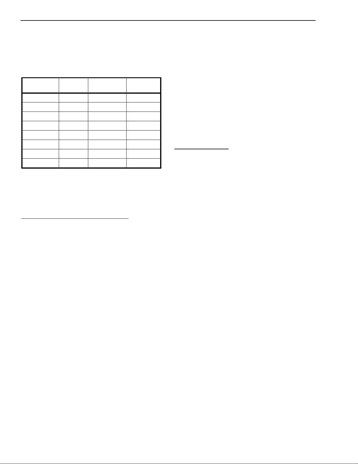
Table 1 gives the standard DTMF frequencies, the
coefficient required to generate the closest
frequency, the actual frequency generated and the
percent deviation of the generated tone from the
nominal.
Frequency
(Hz)
COEF
Actual
Frequency%Deviation
697 59h 695.3 -.20%
770 63h 773.4 +.40%
852 6Dh 851.6 -.05 %
941 79h 945.3 +.46%
1209 9Bh 1210.9 +.20%
1336 ABh 1335. 9 .00%
1477 BD h 1476. 6 -.03%
1633 D1h 1632.8 -.01%
Ta ble 1
DTMF Signal to distortion:
The sum of harm onic and no is e po w er in th e
freque nc y ba nd from 50Hz to 3 50 0H z i s ty pi ca ll y
more t ha n 30 dB below th e p ower in the to n e p ai r. All
individual harmonics are typica lly more than 40dB
below the level of the low group tone.
Tone Ring er and G ain Co ntrol P rogram
A locally generated alerting (ringing) signal is used to
prompt the user when an incoming call must be
answered. The DSP uses the values programmed
into Tone Coefficient Registers 1 and 2 (addresses
23h and 24h) to generate two different squarewave
frequencies in PCM code. The amplitude of the
squarewave frequencies is set to a mid level before
being sent to the receive gain control block. From
there the PCM passes through the decoder and
receive filter, replacing the normal receive PCM data,
on its way to the loudspeaker driver. Both
coefficients are determined by the following
equation:
COEFF = 8000/Frequency (Hz)
where COEFF is a rounded off 8 bit binary integer.
The ringer program switches between these two
frequencies at a rate defined by the 8-bit coefficient
programmed into the Tone Ringer Warble Rate
Register (address 26h). The warble rate is defined
by the equation:
Tone duration (warble frequency
in Hz) = 500/COEFF
An alternate method of generating ringer tones to the
speakerphone speaker is available. With this method
the normal receive speech path through the decoder
and receive filter is uninterrupted to the handset,
allowing an existing conversation to continue. The
normal DSP and Filter/CODEC receive gain control
is also retained by the speech path. When the OPT
bit (DSP Control Register address 1Eh) is set high
the DSP will generate the new call tone according to
the coefficients programmed into registers 23h, 24h
and 26h as before. In this mode the DSP output is no
longer a PCM code but a toggling signal which is
routed directly through the New Call Tone gain
control section to the loudspeaker driver. Refer to
the secti o n ti tle d ‘Ne w Call To ne ’.
Handsfree Program
A half-duplex speakerphone program, fully contained
on chip, provides high quality gain switching of the
transmit and receive speech PCM to maintain loop
stability under most network and local acoustic
environments. Gain switching is performed in
continuous 1.5dB increments and operates in a
complimentary fashion. That is, with the transmit
path at maximum gain the receive path is fully
attenuated and vice versa. This implies that there is
a mid position where both transmit and receive paths
are attenuated equally during transition. This is
known as the idle state.
Of the 64 possible attenuator states, the algorithm
may rest in only one of three stable states; full
receive, full transmit and idle. The maximum gain
values for full transmit and full receive are
programmable through the microport at addresses
20h and 1Dh respectively, as is done for normal
handset operation. This allows the user to set the
maximum volumes to which the algorithm will
adhere. The algorithm determines which path should
maintain control of the loop based upon the relative
levels of the transmit and receive audio signals after
the detection and removal of background noise
energy. If the algorithm determines that neither the
transmit or the receive path has valid speech energy
then the idle state will be sought. The present state
of the algorithm plus the result of the Tx vs. Rx
decision will determine which transition the algorithm
will take toward its next stable state. The time
durations required to move from one stable state to
the next are parameters defined in CCITT
Recommendation P.34 and are used by default by
this algorith m (i.e ., b u ild- u p time , h a ng- ov e r time a nd
switching time).
where 0 < COEFF < 256, a warble rate of 5-20Hz is
suggested.
7-10
Page 9

MT9092
Quiet Code
The DSP can be made to send quiet code to the
decoder and receive filter path by setting the
RxMUTE bit high. Likewise, the DSP will send quiet
code in the transmit (DSTo) path when the TxMUTE
bit is high. Both of these control bits reside in the
DSP Control Register at address 1Eh. When either
of these bits are low, their respective paths function
normally.
HDLC
The High-level Data Link Control (HDLC) block is
located, functionally, between the serial ST-BUS port
and the serial Microcontroller port. This functional
block handles the bit oriented protocol requirements
of layer 2 X.25 packet switching and Q.921 link
access protocols defined by CCITT. The HDLC is
dedicated to D-Channel operation at 16kb/s and
offers buffered access to the serial D-Channel data
through separate 19 byte transmit and receive
FIFOs.
The HDLC generat es and det ects the flags, various
link channel states and abort sequences as well as
performing a cyclic redundancy check on data
packets according to the CCITT defined polynomial.
Lastly, the protocol functions may be disabled to
provide transparent access, of the serial port DChannel, to the microport.
generates flags and appends them to the packet to
be transmitted. The receiver searches the incoming
data stream for flags on a bit-by-bit basis to establish
frame synchronization. The receiver uses flags for
synchronization only and does not transfer them to
the Rx FIFO.
Address F ield
The address field consists of one or two 8-bit bytes
directly following the opening flag. Address, Control
and Information fields are known collectively as the
Data field.
Control Fi eld
The control field consists of one 8-bit byte directly
following the address field. The HDLC does not
distinguish between the control field and the
informatio n field.
Information Field
The information field immediately follows the control
field and consists of N bytes of data where one by te
contains 8 bits. A packet does not need to contain an
information field to be valid. The HDLC does not
distinguish between the control field and the
informatio n field.
Frame Checking Sequence Field
A power up reset (PWRST
via RST (address 0Fh) will cause the HDLC
transceiver to be initialized. This results in the
transmitter and receiver being disabled and all HDLC
registers defaulting to their power reset values.
HDLC Frame Stru cture
A valid HDLC frame begins with an opening flag,
contains at least 16 bits of address, control or
information, ends with a 16 bit FCS followed by a
closing flag. Data formatted in this manner is also
referred to a s a " packet". Refer to Fi gu re 4 .
FLAG DATA FIELD FCS FLAG
One
Byte
n Bytes
(n≥2)
Figure 4 - Frame Format
, pin 6) or a softwar e reset
Two
Bytes
One
Byte
Flag Sequ ence
All HDLC frames start and end with a unique
sequence of 8 bits. This sequence is 0111 1110
(7Eh). The closing flag of one frame can be the
opening flag of the next frame. The transmitter
The 16 bits preceding a closing flag are the FCS
field. A cyclic redundancy check utilizing the CRCCCITT standard generator polynomial X
+1 produces the 16-bit FCS. In the transmitter the
FCS is calculated on all bits of the address, control
and information fields. The complement of the FCS
is transmitted, most significant bit first, in the FCS
field. The receiver calculates the FCS on the
incoming packet's address, control, information and
FCS fields and compares the result to 'F0B8'. This
result verif ies no transm ission errors occu rred. If the
packet, between flags, is also at least 32 bits in
length then t he address, control and information field
data are entered into the receive FIFO minus the
FCS which is discarded.
16
+ X12 +X
Order of Bit Transmission
Address, control and information field data are
entered into the transmit FIFO. This data is then
transmitted and received on the serial bus least
significant bit first. The FCS is sent most significant
bit first on the serial bus. Note that it is the
complement of the calculated FCS which is
transmitted. The HDLC does not distinguish
ADDRESS/CONTROL/INFORMATION bytes except
5
7-11
Page 10

MT9092
to determine if the packet is of minimum valid length.
These fields are transferred transparently through
the FIFO's.
Data Transparency (Ze ro inserti on/d eletio n)
Transparency ensures that the contents of a data
packet do not imitate a flag, go-ahead, frame abort
or idle channel. The content s of a transmitted frame,
between the flags, is examined on a bit-by-bit basis
and a 0 bit is inserted after all sequences of five
contiguous 1 bits (including the last five bits of the
FCS). Upon receiving five contiguous 1s within a
frame the re ce ive r d ele te s th e fo llow i n g 0 bit.
Invalid Frames
A frame is invalid if one of the following four
conditions exists. Inserted zeros are not part of a
valid bit count:
1. If the FCS pattern generated from the received
data does not match the 'F0B8' pattern then the
last data byte of the packet is written to the
receive FIFO with a 'bad packet' indication.
2. A short frame exists if there are less than 25 bits
between the flags. Short frames are ignored by
the receiver and nothing is written into the
receive FIFO.
3. P ackets which are at least 25 bits in length but
less than 32 bits (between the flags) are also
invalid. In this case the data is written to the
FIFO but the last byte is tagged with a 'bad
packet' indication.
4. If a frame abort sequence is detected the packet
is invalid. Some or all of the current packet will
reside in the receive FIFO, assuming the packet
length before t he abort sequence was at least 26
bits long.
Frame Ab ort
The transmitter will abort a current packet by
substituting a zero followed by seven contiguous 1s
in place of the normal data. The receiver will abort
upon reception of seven contiguous 1s occurring
between the flags of a packet which contains at least
26 bits.
Note that should the last receive byte before the
frame abort end with contiguous 1s, these are
included in the seven 1s required for a receiver
abort. This means that the location of the abort
sequence in the receiver may occur before the
location of the abort sequence in the originally
transmitted packet. If this happens, t hen the last data
written to the receive FIFO will not correspond
exactly with the last byte received before the frame
abort.
Interframe T ime F ill and L ink Cha nne l State s
When the HDLC transmitter is not sending packets it
will wait in one of two states.
Interframe Time Fill: This is a continuous series of
flags occurring between
frames indicating that the
channel is active but that no
data is being sent.
Idle: An idle channel occurs when at least fifteen
contiguous 1s are transmitted or received.
In both cases the transmitter will exit the wait state
when data is loaded into the transmit FIFO.
Go-Ahead
A go-ahead is defined as the pattern ‘011111110’
(contiguous 7F’s) and is the occurrence of a frame
abort sequence followed by a zero, outside of the
boundaries of a normal packet. Being able to
distinguish a proper (in packet) frame abort
sequence from one occurring outside of a packet
allows a higher level of signalling protocol which is
not part of the HDLC specifications.
Transmitter
Following initialization and enabling, via the HTxEN
bit (address 03h), the transmitter is in the Idle
Channe l State (Mark Idle ). Interf rame time fill may
be selected by setting the Mark Idle bit (address 03h)
high. The transmitter remains in its programmed
state until data is written to the Tx FIFO. The
transmitter will then proceed as follows:
1) If the transmitter is in the idle state the present
byte of ones will be completely transmitted
before the opening flag and packet data is
sent.
2) If the transmitter is in the interframe time fill
state the flag currently being transmitted will be
used as the opening flag followed by the
packet data.
To assist in loading multiple packets into the transmit
FIFO the last packet byte is tagged with either EOP
(to indicate the end of the current packet) or FA.
Control Register 1 (address 03h) bits EOP (end of
7-12
Page 11

MT9092
packet) and FA (frame abort) are set before writing
the last packet byte to the Tx FIFO. The act of
loading the last packet byte will then automatically
reset the EOP and FA bits. Tx FIFO bytes are
continuously transmitted until the FIFO is empty, by
which time an EOP or FA tag should have been
encounte r ed b y the transmitter.
After the last bit of the EOP byte has been
transmitted a 16 bit FCS is sent followed by a closing
flag. When multiple packets of data are loaded into
the Tx FIFO only one flag is sent between packets.
When the transmitter encounters a byte tagged FA
then a frame abort sequence is sent instead of the
tagged byte. All bytes previous to but not including
the tagged byte are sent.
The transm itter r eturns to its p rogramm ed wai t state
after concluding the transmission of EOP or FA if the
Tx FIFO is empty.
Transmit FIFO Status
The transmit FIFO is 19 bytes deep (address 02h).
As data is loaded into (from the microport) and
extracted from (via the serial port) the Tx FIFO the
present 'fill state' can be monitored using the Txstat1
and Txstat2 bits found in the HDLC Status Register
(address 04h). These states are encoded as shown
in Table 2. Note that the FIFO emptying threshold,
where an interrupt (TxFL if unmasked) will occur, can
be set to a low level 4 (default) or to a high level 14
by the Fltx bit in the HDLC Control Register 2
(address 05h).
Command/Address byte which indicates a microport
read of address 07h. Since all interrupts are
generated by the occurrence of an HDLC event (i.e.,
a transition), this register informs that an event has
occurred but does not guarantee that it is still valid.
To determine current validity the HDLC Status
Register (address 04h) should be read. Due to the
asynchronous nature of the interrupts an interrupt
occurring during a read of the Interrupt Status
register will be held until the read cycle is over,
unless it is an interrupt which is already valid.
There are three interrupts associated with the
transmitter.
TEOP Transmit End Of Packet:
Set when the transmitter has finished
sending the closing f lag of a packet or
after an abort sequence has been
completed.
TxFL Transmit FIFO Low:
Set when a transit ion from 5 to 4 bytes
in the Tx FIFO has occurred. This is an
early warning to the microprocessor
that the FIFO is emptying and should
be serviced before it empties
completely; a condition which will
result in a transmit underrun unles s an
EOP or FA byte has been written to the
FIFO. By setting the Fltx bit (address
05h) high the FIFO emptying condition
will occur at the transition from 15 to 14
bytes. This will allow the microport
more time to react to this interrupt
condition.
A Tx FIFO underrun occurs if the Tx FIFO empties
without the oc currence of an EOP or FA tagged byte.
A frame abort sequence is automatically transmitted
under this condition.
Transm it Interrupts
The HDLC Interrupt Enable Register (address 06h)
is used to select (unmask) only those interrupts
which are deemed important to the microprocessor.
After a PWRST
be cleared causing all interrupts to be masked.
All selected i n te rrup t e vents will c ause the IRQ pin to
become active. Unselected interrupt events will not
cau se IRQ
still be represented by the appropriate bit in the
HDLC Interrupt Status Register (address 07h). This
register must be read after receiving an IRQ
be polled at any time. The IRQ
coincident with the first SCLK falling edge following a
or software RST all enable bits will
to become active however, the event will
or may
output pin is reset
Txunder Transmit underrun:
Set when the Tx FIFO empties without
the occurrence of an EOP or FA
tagged byte. A frame abort sequence
is automatically transmitted under this
condition. Note that this register bit
position is shared with the frame abort
(FA) interrupt (see receive interrupts).
For this b it to r eflect T xund er t he Ints el
bit in Control Register 2 (address 05h)
must be set high.
Disabling, Res et, Transparent Operat ion an d CRC
Disabling the transm itter via the HTxEn bit will occur
after the current packet is completely transmitted.
The status and Interrupt registers may still be read
and the Tx FIFO and control registers written while
the transm it te r is d isa ble d .
7-13
Page 12

MT9092
The Tx FIFO may be reset by setting the Txfrst bit in
the HDLC Control Register 2 (address 05h). The
HDLC Status Register will identify the Tx FIFO as
being empty although the actual data in the FIFO will
not be reset. Txfrst will be cleared by the next write
to the Tx FIFO.
Transparent data may be sent by setting the TRANS
bit (address 03h) high. The transmitter will no longer
generate the flag, abort and idle sequences, nor will
it insert zeros and append the FCS. Data will still be
transmitted LSB first. If there is no data in the Tx
FIFO or the Tx FIFO empties the last byte
transmitted will be repetitively sent until new data is
presented to the FIFO. It will t ake typically two STBUS frames, af ter writing TRANS, before this mode
begins. Note that CH
Transmission of the FCS field CRC may be inhibited
using the Tcrci (Transmit Crc Inhibit) bit at address
05h. W hile this bit is set the o pe n in g fl a g fo ll o we d b y
the data fields and closing flag is transmitted,
including zero insertion, but the calculated CRC is
not. This allows the processor to insert the CRC as
part of the data field. This usage is for V.120 terminal
adaptation for synchronous protocol sensitive UI
frames.
Receiver
Following initialization and enabling, via the HRxEN
bit at address 03h, the receiver begins clocking in
serial data checking for flags (0111 1110), go-aheads
( 0111 1111 0), and idl e c hannel states (at l eas t f ifteen
contiguous ones). Upon detecting a flag the receiver
synchronizes itself to the data stream and begins
calculating the CRC. If the packet length, between
the flags and after zero deletion, is less than 25 bits
the packet is ignored and nothing is written to the Rx
FIFO. If the packet length, after zero deletion, is
between 25 and 31 bits a last byte, bad packet
indication is written into the Rx FIFO.
EN must also be set.
0
Idle Channel
When the receiver detects at least 15 contiguous
ones it declares an idle channel condition exists and
sets the IdleChan bit in the HDLC status register
high (address 04h). This bit remains set until the
received condition changes.
If address recognition is required, Receive Address
Recognition Registers 1 and/or 2 (addresses 00h
and 01h respectively) are loaded with the desired
address comparison information, the Adrec bit is set
high and A1EN and A2EN are set as required. Bit 0
(A1EN and A2EN) of both recognition registers is
used as an enable for that by te. When either of these
bits are low their respective address mask
information is ignored. In this way either or both of
the first two received bytes can be compared to the
expected mask values. Only those packets passing
the appropriate comparison test will be loaded into
the Rx FIFO. The appropriate comparison test
(single/dual byte address, All-call) is defined by the
logic state of bit 0 of the first byte received after the
opening flag.
Bit 0 of the first received address byte (address
extension bit) is monitored to determine if a single or
dual byte address is being received.
1. If the address extension bit is 1 then a single
byte address is being received. If A1EN is high
the stored bit mask (Adr11 - Adr16 and
sometimes Adr10) is compared to the received
first address byte. Any packet failing this
address comparison will not be stored in the Rx
FIFO except for the All-call condition. A1EN
must be set high for a single-byte All-call
(11111111) address to be recognized. The
second mask byte is ignored. Seven bits of
address comparison may be realized for single
byte recognition by setting the SEVEN bit
(address 05h) high. This mode will then include
Adr10 as part of the mask information. The first
received byte must also have bit 0 set to a 1
indicating single byte addressing.
2. If the address extension bit is 0 then a two byte
address is being received and the six most
significant bits of the first received byte are
compared. The seven most signif icant bits of the
second received byte are compared (Adr20 Adr26, note A2EN must be set high also). Any
packet failing this address comparison will not
be stored in the Rx FIFO. An All-call condition
(1111111x) is also monitored for in the s econd
received address byte and, if found, the first and
second byte masks are ignored (not compared
with the mask byte). Packets addressed with Allcall are written into the Rx FIFO.
Address Recognition
When Adrec (HDLC Control Register 1, address
03h) is low all valid received packets, regardless of
the address field inform ation, are loaded into the Rx
FIFO.
7-14
In CCITT Q.921 parlance the Adr11 - Adr16 bits are
defined as Sapi0 - Sapi5 (Service Access Point
Identifier n). Adr10 is defined as C/R (Command/
Response). Adr20 - Adr26 are defined as Tei0 - Tei6
(Terminal Endpoint Identifier n).
Page 13

MT9092
Receive Byte Status
As each received pack et byte is wr itten into th e Rx
FIFO two bits are appended to indicate the status of
that byte. As these bytes are read from the Rx FIFO
the status bits are made available to the
microprocessor in the HDLC Status Register
(address 04h) as RxBS1 and RxBS2. Since the
information contained in RxBS1 & RxBS2 pertains to
the byte about to be read from the Rx FIFO, it is
important that this information be read before
reading the data byte from the FIFO. RxBS1 and
RxBS2 are encoded as shown in Table 2. A good
packet indication means a good FCS and no frame
abort whereas a bad packet indication means either
an incorrect FCS or a frame abort occurred.
Receive F IFO Status
The receive FIFO is 19 bytes deep (address 02h). A s
data is loaded into (from the serial port) and
extracted from (via the microport) the Rx FIFO the
present 'fill state' can be monitored using the Rxstat1
and Rxstat2 bits found in the HDLC Status Register
(address 04h). These states are encoded as shown
in Table 2. Note that the FIFO filling threshold, where
an interrupt (RxFf if unmasked) will occur, can be set
to a high level 15 (default) or to a low level 5 by the
Flrx bit in the HDLC Control Register 2 (address
05h).
In the case of an Rx FIFO overflow, an attempt by
the receiver to write data into an already full FIFO,
the receiver is disabled causing it to stop writing to
the Rx FIFO. The remainder of the current receive
packet is therefore ignored. The receiver will be reenabled when the next flag is detected but will
overflow again if the Rx FIFO level has not been
reduced to less than full. If two 'first byte' (RxBS1
and RxBS2) conditions are observed in the FIFO
without an intervening 'last byte' then an overflow
occurred for the first packet.
Receive Interrupt s
The HDLC Interrupt Enable Register (address 06h)
is used to select (unmask) only those interrupts
which are deemed important to the microprocessor.
After a PWRST
be cleared causing all interrupts to be masked.
or software RST all enable bits will
RxBS2, Are status bits from the Rx FIFO.
RxBS1 RxBS2
1 1 last byte (bad packet)
0 1 first byte
1 0 last byte (good packet)
0 0 packet byte
Note - If two consecutive first byte signals are received without an inte rven ing last byte, then an
overflow has occurred and the first packet (or packets) are bad. A bad packet indicates that
either a frame abort had occurred or the FCS did not match.
- On power-up these bits are in an indeterminate state until the first byte is writte n to Rx FIFO.
Txstat2,
Txstat1 These two bits are encoded to indicate the present state of Tx FIFO. This is an asynchronous
event.
Txstat2
0 0 TxFULL
0 1 5 OR MORE BYTES (15 if Fltx set)
1 1 4 OR LESS BYTES (14 if Fltx set)
1 0 TxEMPTY
Rxstat2,
Rxstat1 These two bits are encoded to indicate the present state of Rx FIFO. This is an asynch ronous
event.
Rxstat2
0 0 RxEMPTY
0 1 14 OR LESS BYTES (4 if Flrx set)
1 1 15 OR MORE BYTES (5 if Flrx set)
1 0 RxOVERFLOW EXISTS
RxBS1 Byte stat us
Txstat1 Tx FIFO Status
Rxstat1 Rx FIFO Status
Ta ble 2 - HDLC S tatus Bits
7-15
Page 14

MT9092
All selected interrupt events will cause the IRQ pin to
become active. Unselected interrupt events will not
cau se IRQ
still be represented by the appropriate bit in the
HDLC Interrupt Status Register (address 07h). This
register m ust be read after receiving an IRQ
be polled at any time. The IRQ output pin is reset
coincident with the first SCLK falling edge following a
Command/Address byte which indicates a microport
read of address 07h. Since all interrupts are
generated by the occurrence of an HDLC event (i.e.,
a trans ition), this r egister infor ms that an event has
occurred but does not guarantee that it is still valid.
To determine current validity the HDLC Status
Register (address 04h) should be read. Due to the
asynchronous nature of the interrupts an interrupt
occurring during a read of the Interrupt Status
register will be held until the read cycle is over,
unless it is an interrupt which is already valid.
There are six interrupts associated with the receiver.
GA Go Ahead:
EOPD End Of Packet Detect:
EopR End of packet Read:
FA Frame Abort:
RxFf - Receive FIFO filling:
to become active however, the event will
or may
Set when a go-ahead pattern
( 0 1111111 0) h a s be e n de t e c te d b y t h e
receiver.
Set when an end of packet byte has
been written into the Rx FIFO by the
receiver. This event may be due to
receiving a closing flag, an abort
sequence or an invalid packet.
Set when the next byte to be read from
the Rx FIFO is the last byte of a
packet or when a read to an empty Rx
FIFO has occurred.
Set when a frame abort sequence is
received during packet reception. The
aborted packet must contain a
minimum of 26 bits for the FA
sequence to be recognized. Not e that
this register bit position is shared with
the transmitter under-run (Txunder)
interrup t (see transmit inte rrupts). For
this bit to reflect FA the Intsel bit in
Control Register 2 (address 05h) must
be set low.
Set when a transition from 14 to 15
bytes in the Rx FIFO has occurred.
This is an early warning to the
microprocessor that the FIFO is filling
and should be serviced before it
becomes completely full; a condition
which may result in a receive overflow
condition. By setting the Flrx bit
(address 05h) high the FIFO filling
condition will occur when a transition
from 4 to 5 bytes occurs. This will
allow the microport more time to react
to this interrupt conditi o n.
RxOvfl - Re c eiv e F IFO O v e rflo w:
Set when the receiver attempts to
write data into an already full Rx FIFO.
Under this condition the HDLC will
disable the receiver until a new flag is
detected. See also Receive FIFO
Status.
Disabling, Reset and Transparent Operation
Disabling of the receiver via the HRxEn bit will occur
after the current packet is completely loaded into the
Rx FIFO. Disabling can occur during packet
reception if no bytes have been written to the Rx
FIFO yet. The Rx FIFO, status and Interrupt registers
may still be read and control registers written while
the receiver is disabled. Note that the receiver
requires the reception of a flag before processing a
packet, thus if the receiver is enabled in the middle
of an incoming packet it will ignore that packet and
wait for th e next complete on e.
The Rx FIF O may be reset b y setting the R xfr st bit in
the HDLC Control Register 2 (address 05h). The
receiver will be disabled until reception of the next
flag. The Status Register will identify the Rx FIFO as
being empty although the actual data in the FIFO will
not be reset. Rxfrst will be cleared by the reception
of the next received flag pattern.
Data may be received transparently by setting the
TRANS bit (address 03h) high. Timing control bit
CH
EN must also be set. The receiver will disable
0
protocol functions such as flag/abort/go-ahead/idle
detection, zero deletion, CRC calculation and
address comparison. Data is shifted into the Rx FIFO
in a byte-wide format. In transparent mode when an
Rx FIFO overflow condit ion occurs the receiver will
continue to write data into the Rx FIFO, overwriting
the last byte. The overflow interrupt condition can
only be detected again if the Rx FIFO is reset (Rxfrst
bit at address 05h) since normally the overflow
condition is cleared by the reception of the next flag
and transparent data is unlikely to emulate a flag.
Also, the Rxfrst bit itself will have to be reset by
writing it low since it is usually reset automatically by
the occu rr en c e of th e ne xt flag.
7-16
Page 15
Transducer Interfaces
MT9092
Four standard telephony transducer interfaces are
provided by the HPhone-II. These are:
➧ The handset microphone inputs (transmitter),
pins M+/M- and the speakerphone microphone
inputs, pins MIC+/MIC-. The transmit path is
muted/not-muted by the MIC EN control bit.
Selection of which input pair is to be routed to
the transmit filter amplifier is acomplished by the
MIC/HNSTMIC
control bit. Both of these reside
in the Transducer Control Register (address
0Eh). The nominal transmit path gain may be
adjusted to either 6.1dB (suggested for µ-Law)
or 15.4dB (suggested for A-Law). Control of this
gain is provided by the MICA/u
control bit
(General Control Register, address 0Fh). This
gain adjustment is in addition to the
programmable gain provided by the transmit
filter and DSP.
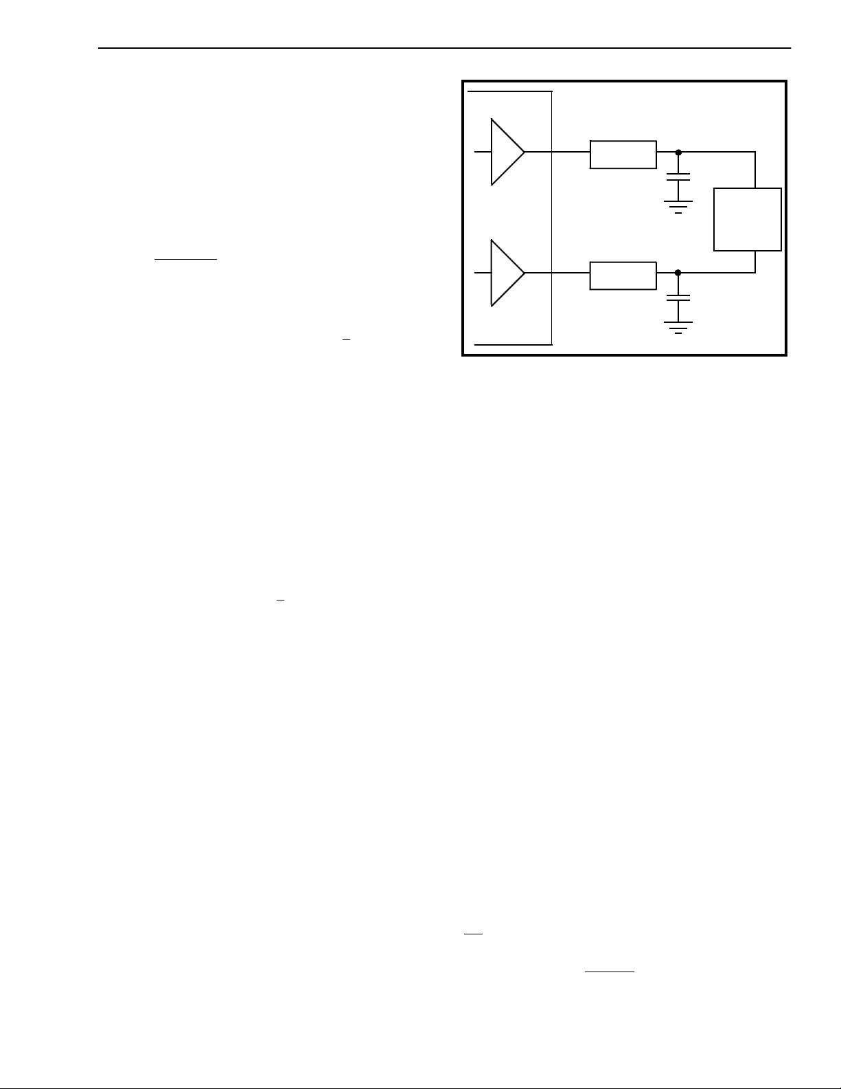
➧ The handset speaker outputs (receiver), pins
HSPKR+/HSPKR-. This internally
compensated, fully differential output driver is
capable of driving the load shown in Figure 5.
This output is enabled/disabled by the HSSPKR
EN bit residing in the Transducer Control
Register (address 0Eh). The nominal handset
receive path gain may be adjusted to either
-12.3dB (suggested for µ-Law) or -9.7dB
(suggested for A-Law). Control of this gain is
provided by the RxA/u
control bit (General
Control Register, address 0Fh). This gain
adjustment is in addition to the programmable
gain provided by the receive filter and DSP.
➧ The loudspeaker outputs, pins SPKR+/SPKR-.
This internally compensated, fully differential
output driver is capable of directly driving 6.5vpp
into a 40 ohm load. This output is enabled/
disabled by the SPKR EN bit residing in the
Transducer Control Register (address 0Eh). The
nominal gain for this amplifier is 0.2dB.
HSPKR+
75 Ω
1000 pF
MT9092
75 Ω
HSPKR-
150 ohm
load
(speaker)
1000 pF
ground
Figure 5- H ands et Spea ker Dr iver
LCD
A twelve segment, non-multiplexed, LCD display
controller is provided for easy implementation of
various set status and call progress indicators. The
twelve output pins (S
) are used in conjunction with
n
12 segment control bits, located in LCD Segment
Enable Registers 1& 2 (addresses 12h and 13h), and
the BackPlane output pin (BP) to control the on/off
state of each segment individually.
The BP pin drives a continuous 62.5Hz, 50% duty
cycle squarewave output signal. An individual
segment is controlled via the phase relationship of its
segment driver output pin with respect to the
backplane, or common, driver output. Each of the
twelve Segment Enable bits corresponds to a
segment output pin. The waveform at each segment
pin is in-phase with the BP waveform when its
control bit is set to logic zero (segment off) and is
out-of-phase with the BP waveform when its control
bit is set to a lo gic high ( segment on). Refer to the
LCD Driver Characteristics for pin loading
information.
C-Channel
Access to the internal c ontrol and status registers of
Mitel bas ic rate, layer 1, tra nsceivers is thro ugh the
ST-BUS Control Channel (C-Channel), since direct
microport access is not usually provided, except in
the case of the SNIC (MT8930). The HPhone-II
provides asynchronous microport access to the STBUS C-Channel information on both DSTo and DSTi
via a double-buffered read/write register (address
14h). Da ta written to thi s address is transmitted o n
the C-Channel every frame when enabled by CH
1
EN
(see ST-BUS/Timing Con t rol ) .
Microport
A serial microport, compatible with Intel MCS-51
(mode 0) specifications, provides access to all
HPhone-II internal read and write registers. This
microport consists of three pins; a half-duplex
transmit/receive data pin (DATA1), a chip select pin
(CS
) and a synchronous data clock pin (SCLK).
On power-u p res et (PWRST
) or with a s o ftw a re reset
(RST), the DATA1 pin becomes a bidirectional
(transmit/receive) serial port while the DATA2 pin is
internally disconnected and tri-stated.
7-17
Page 16
MT9092
All data transfers through the microport are two-byte
transfers requiring the transmission of a Command/
Address byte followed by the data byte written or
read from the addressed register. CS
must remain
asserted fo r th e duration of this t wo - by te t ra n sfer. As
shown in Figure 6, the falling edge of CS
indicates to
the HPhone-II that a microport transfer is about to
begin. The first 8 clock cycles of SCLK after the
falling edge of CS
are always used to receive the
Command/Address byte from the microcontroller.
The Command/Address byte contains information
detailing whether the second byte transfer will be a
read or a write operat ion and of what address. The
next 8 clock cycles are used to transfer the data byte
between the HPhone-II and the microcontroller. At
the end of the two-byte transfer CS
is brought high
again to terminate the se ssion. The rising edge of CS
will tri-state the output driver of DATA1 which will
remain tr i- st ated as long as CS
is high.
Receive data is sampled and transmit data is made
available on DATA1 concurrent with the falling edge
of S CLK.
An open-drain interrupt request (IRQ) output
provides a method for interrupting the
microcontroller when an unmasked HDLC event
occurs within the HPhone-II. IRQ
remains active until
the HDLC Interrupt Status Register is read or a
(hardware/software) reset occurs. More detail is
provided in the section pertaining to the HDLC
functional block.
Lastly, provision is made to seperate the transmit
and receive data streams onto two individual pins.
This control is given by the DATASEL pin in the
General Control Register (address 0Fh). Setting
DATA SEL logic high will cause DATA1 to become the
data receive pin and DATA2 to become the data
transmit pin. Only the signal paths are altered by
DATASEL; internal timing remains the s ame in both
cases. Tri-stating on DATA2 follows CS
as it does on
DATA1 when DATASEL is logic low. Use of the
DATASEL bit is intended to help in adapting Motorola
(SPI) and National Semiconductor (Micro-wire)
microcontrollers to the HPhone-II. Note that whereas
Intel processor serial ports transmit data LSB first
other processor serial ports, including Motorola,
transmit data MSB first. It is t he responsibility of the
microcontroller to provide LSB first data to the
HPhone-II.
ST-BUS/Timing Control
A serial link is required for the transport of data
between the HPhone-II and the external digital
transmission device. The HPhone-II utilizes the STBUS architecture defined by Mitel Semiconductor.
Refer to Mitel Application Note MSAN-126. The
HPhone-II ST-BUS consists of output and input
serial data streams, DSTo and DSTi respectively, a
synchronous clock signal C4i
.
F0i
, and a framing pulse
COMMAND/ADDRESS DATA INPUT/OUTPUT COMMAND/ADDRESS
DATA 1
Receive
DATA 1 or DATA 2
Transmit
SCLK
CS
➀
➁
➂
➃
➄
D0D1D2D3D4D5D6D
➁
➂
Delays due to MCS-51 internal timing which are transparent.
The HPhone-II: -latches received data on the falling edge of SCLK
The falling edge of CS
byte is always data followed by CS
A new COMMAND/ADDRESS byte may be loaded only by CS
The COMMAND/ADDRESS byte contains:
-outputs transmit data on the falling edge of SCLK
indicates that a COMMAND/ADDRESS byte will be transmitted from the microprocessor. The subsequent
➄
➀
D0D1D2D3D4D5D6D
7
D0D1D2D3D4D5D6D
returning high.
1 bit - Read/Write
6 bits - Addressing Data
1 bit - Not used, write logic "0"
Figure 6 - S erial Port Rela tive Tim ing
➀
7
7
➃
➂
cycling high then low again.
D
7
0A5A4A3A2A1A0R/W
➃
D0D1D2D3D4D5D6D
D0D1D2D3D4D5D6D
7
7
D
0
7-18
Page 17
MT9092
The data streams operate at 2048kb/s and are Time
Division Multiplexed into 32 identical channels of
64kb/s bandwidth. Frame Pulse (a 244nSec low
going pulse) is used to parse the continuous serial
data streams into the 32 channel TDM frames. Each
frame has a 125µSecond period translating into an 8
kHz frame rate. Valid frame pulse occurs when F0i
logic low coincident with a falling edge of C4i
is
. C4i
has a frequency (4096MHz) which is twice the data
rate. This clock is used to sample the data at the 3/4
bit-cell position on DSTi and to make data available
on DSTo at the start of the bit-cell. C4i
is also used
to clock the HPhone-II interna l functions (i.e., DS P,
Filter/CODEC, HDLC) and to provide the channel
timing requirements.
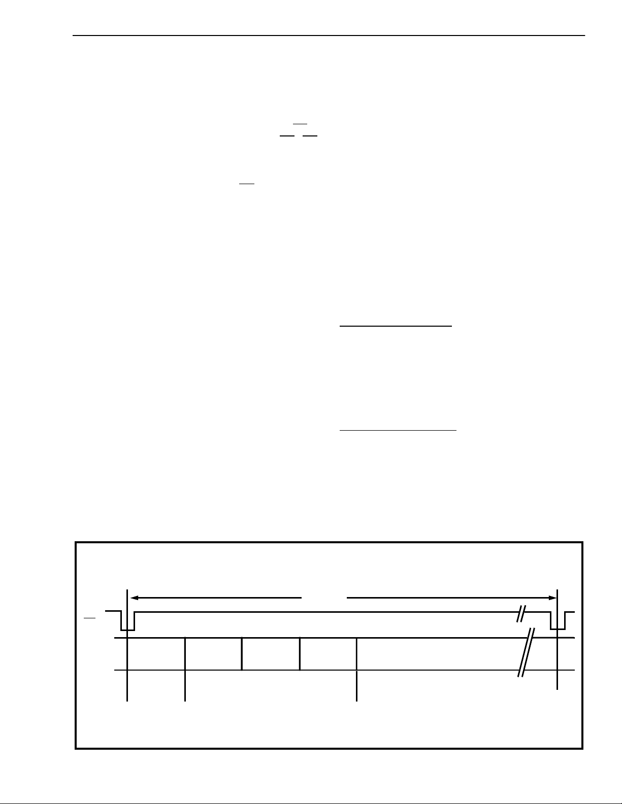
The HPhone-II uses only the first 4 channels of the
32 channel frame. These channels are always
defined, beginning with the first channel after frame
pulse, as shown in Figure 7 (DSTi and DSTo channel
assignments). Channels are enabled independantly
by the four c ontrol bits Ch
En -Ch3En residing in the
0
Timing Control Regis ter (address15h).
Ch0EN - D-Channel
Channel 0 conveys the D-Channel HDLC
information. Since this function is dedicated to
16kb/s operation, only the first two bits (LSB's)
of the octet are required; the remaining six bits
of the D-Channel octet carry no information and
are tri-stated. When CH
EN is high, HDLC data
0
is transmitted on DSTo. When low, DSTo is
forced to logic 0 fo r the two least signi ficant bit
positions. Incoming DSTi data is always
routed to the HDLC block regardless of this
control bit's logic state.
Ch1EN - C-Channel
Channel 1 conveys the control/status
information for Mitel’s layer 1 transceiver. The
full 64kb/s bandwidth is available and is
assigned according to which transceiver is
being used. Consult the data sheet for the
selected transceiver for its bit definitions and
order of bit transfer. When this bit is high
register data is transmitted on DSTo. When low,
this timeslot is tri-stated on DSTo. Receive CChannel data (DSTi) is always routed to the
register regardless of this control bit's logic
state. C-channel data is transferred on the STBUS MSB first by t he HPhone-II.
EN and Ch3EN - B1-Channel and B2-Channel
Ch
2
Channels 2 and 3 are the B1 and B2 channels,
respectively. These bits (Ch
EN and Ch3EN)
2
are used to enable the PCM channels from/to
the HPhone-II as required.
Transmit PCM on D STo
When high, PCM from the Filter/CODEC and DSP is
transmitted on DSTo in the selected ST-BUS
channel. Wh en low, DSTo is force d to logic 0 for th e
corresponding timeslot. If both Ch
EN and Ch3EN
2
are enabled, default is to channel 2.
Receive PCM from DS Ti
When high, PCM from DSTi is rout ed to the DSP and
Filter/CODEC in the associated channel. If both
EN and Ch3EN are enabled the default is to
Ch
2
channel 2.
F0i
DSTi,
DSTo
CHANNEL 0
D-channel
LSB first
for D-
Channel
CHANNEL 1
C-channel
CHANNEL 2
B1-channel
MSB first for C, B1 - & B2-
Chan nels
Figure 7 - ST-BUS Channel Assignment
125 µs
CHANNEL 3
B2-channel
CHANNELS 4 - 31
Not Used
7-19
Page 18

MT9092
New Call Tone
The New Call Tone Generator produces a frequency
shifted square-wave used to toggle the speaker
driver outputs. This is intended for use where a
ringing signal is required concurrently with an
already established voice conversation in the
handset.
Programming of the DSP for New Call generator is
exactly as is done for the tone ringer micro-program
except that the OPT bit (DSP Control Register,
address 1Eh) is set high. In this mode the DSP does
not produce a frequency shif ted squarewave output
to the filter CODEC section. Instead the DSP uses
the contents of the tone coefficient registers, along
with the tone warble rate register, to produce a gated
squarewave control signal output which toggles
between the programmed frequencies. This control
signal is routed to the New Call Tone block when the
NCT E N con trol bi t is s et (Gen eral Contr ol Re gist er,
address 0Fh). NCT EN also enables a separate gain
control block, for controlling the loudness of the
generated ringing signal. With the gain control block
set to 0dB the output is at maximum or 6 volts p-p.
Attenuation of the applied signal, in three steps of 8
dB, provide the four settings for New Call tone (0, -8,
-16, -24 dB). The NCT gain bits (NCTG
-NCTG1)
0
reside in the FCODEC Gain Control Register 2
(address 0Bh).
Watchdog
To maintain program integrity an on-chip watchdog
timer is provided for connection to the
microcontroller reset pin. The watchdog output WD
(pin 17) goes high while the HPhone-II is held in
reset via the PWRST
(pin 6). Release of PWRST wil l
cause WD to return low immediately and will also
start the watchdog timer. The watchdog timer is
clocked on the falling edge of F0i
this input, a l o n g with V
, for operation.
DD
and requires only
If the watchdog res e t w o rd is w ritten to th e w at ch d og
register (address 11h) after PWRST is released, but
before the timeout period (T=512mSec) expires, a
reset of the timer results and WD will remain low.
Thereafter, if the reset word is loaded correctly at
intervals less than 'T' then WD will continue low. The
first break from this routine, in which the watchdog
register is not written to within the correct interval or
it is written to with incorrect data, will result in a high
going WD output after the current interval 'T' expires.
WD will then toggle at this rate until the watchdog
register is again writte n to correctly.
5-BIT WATCHDOG RESET WORD
W4 W3 W2 W1 W0
XXX01010
x=don’t care
Test Loops
Detail LBio and LBoi Loopback Register (address
16h)
LBio Setting this bit causes data on DSTi to be
looped back to DSTo directly at the pins. The
appropriate channel enables Ch
EN -Ch3EN
0
must also be set.
LBoi Setting this bit causes data on DSTo to be
looped back to DSTi directly at the pins.
7-20
Page 19

HPhone-II Register Map
MT9092
Address
(Hex)
00 HDLC ADDRESS RECOGNITION REGISTER 1 VERIFY
01 HDLC ADDRESS RECOGNITION REGISTER 2 VERIFY
02 HDLC TRANSMIT FIFO HDLC RECEIVE FIFO
03 HDLC CONTROL REGISTER 1 VERIFY
04 NOT USED HDLC STATUS RE GI S TER
05 HDLC CONTROL REGISTER 2 VERIFY
06 HDLC INTERRUPT ENAB LE REGIST ER VERIFY
07 NOT USED HDLC INTERRUPT STATUS REG ISTER
08 RESERVED RESERVED
09 RESERVED RESERVED
0A FCODEC GAIN CON TROL REGIS TER 1 VERIFY
0B FCODEC GAIN CON TROL REGIS TER 2 VERIFY
0C RESERVED RESERVED
0D RESERVED RESERVED
0E TRANSDUCER CONTROL REGISTER VERI FY
WRITE READ
0F GENERAL CONTROL REGISTER VERIFY
10 RESERVED RESERVED
11 WATCHDOG REGISTER NOT USED
12 LCD SEGMENT ENABLE REG ISTER 1 VERI FY
13 LCD SEGMENT ENABLE REG ISTER 2 VERI FY
14 C-CHANNEL REGISTER (to DSTo) C-CHANNEL REGISTER (from DSTi)
15 TIMING CONT ROL RE GI STE R VERI FY
16 LOOP-BACK REGISTER VERIFY
17-1C RESERVED RESERVED
1D RECEIVE GAIN CONTROL RE GI STE R VERI FY
1E DSP CONTROL RE GI ST ER VERIFY
1F RESERVED RESERVED
20 TRANSMIT AUDIO GAIN REGISTER VERIFY
21 TRANSMIT DTMF GAIN REGISTER VERIFY
22 RESERVED RESERVED
23 TONE COEFF IC IENT REGISTER 1 VERIFY
24 TONE COEFF IC IENT REGISTER 2 VERIFY
25 RESERVED RESERVED
26 TONE RINGER WARBLE RATE REGISTER VERI FY
27-3F RESERVED RESERVED
7-21
Page 20
MT9092
Register Summary
reference to review each of the control/status bit
definitions without the need to locate them in the text
This section contains a complete listing of the
of the functional block descriptions.
HPhone-II register addresses, the control/status bit
mapping associated with each register and a
definition of the function of each control/status bit.
The Register Summary may be used for future
HDLC Address Recog ni tion Reg ister 1 ADDRESS = 00h WRITE/READ VERIFY
Power Reset Value
Adr16 Adr15 Adr14 Adr13 Adr11 Adr10 A1ENAdr12
0000 0000
76543210
Adr 16-11 A si x bit ma s k use d to i nterrogate the f irst byte of t he re ceived address. Adr16 is MSB. In t he Q.921 sp ecifi cati on t he se
Adr 10 This bit is use d in ad dre ss co m parison if a se ven b it addr e ss is be ing che c ked fo r (Con tro l bit Seve n of Con trol Reg ister 2
A1EN Wh en this bit is high, this six (or seven) bit mas k is used in address comparison of the first address byte. If address
bits are defined to be Sapi5-0.
is set). In the Q.921 specification this bit is defined to be C/R (Command/Response).
recognition is enab led, any packet f ai ling the addre s s comp ariso n will not be stored in th e RX FIFO. A1EN must be high
for All-call (1111111) address recognition for single byte address. When this bit is low, this bit mask is ignored in address
comparison.
HDLC Address Recog ni tion Reg ister 2 ADDRESS = 01h WRITE/READ VERIFY
Power Reset Value
Adr26 Adr25 Adr24 Adr23 Adr21 Adr20 A2ENAdr22
0000 0000
76543210
Adr 26-20 A seven bit mask used to interrogate the second byte of the received address. Adr26 is MSB. This mask is ignored (as well
A2EN When this bit is high this seven bit mask is used in address comparison of the second address byte. If address recognition
as first byte mask) i f an All call addre ss (1111111) is rece ived. In the Q.921 specification these b its are defined to be
Tei6-0.
is enabled, any pac ket failing the add ress comparison will not be sto red in the RX FI FO. A2EN m ust be high for All-call
address recognition. When this bit is low, this bit mask is ignored in address comparison.
HDLC Transmit/Receive FIFO Register ADDRESS = 02h WRITE/READ
Power Reset Value
D7 D6 D5 D4 D2 D1 D0D3
Not App li ca bl e
76543210
The Transmitter FIFO is 19 words deep. Each word consists of 8 bits of data from the internal data bus and 2 status bits from CONTROL Register 1 (EOP and FA). If there is data in the Tx FIFO then the lowest data byte in it is loaded into an output shift register for
transmission, and the remaining data shifts down by one word position (Tx FIFO read). A write to a full Tx FIFO will update the top byte
only.
The receiver FIFO is 19 word s deep . During a receive r write , the last 8 bits of a shift register buf fer an d two statu s bits are loade d into
7-22
Page 21
MT9092
HDLC Control Register 1 ADDRESS = 03h WRITE/READ VERI FY
Power Reset Value
000 0 00 00
Adrec HRxEN HTxEN EOP
Mark
Idle
Trans -FA
76543210
Adrec Wh en high this bit will enable addres s recognition. This for ces the receiver to reco gnize only those p ackets having the
HRxEN When low this bit will disable the HDLC receiver. The receiver will disable after the rest of the packet present ly being
HTxEN When low this bit will disable the HDLC transmitter. The transmitter will disable after the completion of the packet presently
EOP Forms a tag o n th e next byte writ ten to th e Tx FIFO a nd whe n set wi ll indi cate an EOP byte to th e tran smitte r wh ich will
FA Forms a tag on the next byte written to Tx FIFO and when set will indica te to the transm itt er th at it should abort th e packe t
Mark Idle Wh en low, the tran smi tte r wil l be in an idle stat e. When h igh it is in an Interframe time f ill sta te . These t wo states will only
Trans When high this bit will enable transparent mode. The HDLC will perform the serial-to-parallel and parallel-to-serial
unique address as programmed in the Receive Address Recognition Register s or if the address is an All-Call address.
When low, all packets are recognized.
received is finished. When high the receiver will be immediately enabled (depending on the state of CHoEN) and will begin
searching for flags, Go-aheads etc.
being transm itted. When high the transmitte r will be immediately enabled (de pending on the state of CHoEN) and will
begin transmitting data, if any, or go to a Mark idle or Interframe time fill state.
transmit a n FCS fol lowing this byte. Th is facil itate s l oadi ng of mul tip le pa cke ts int o Tx FIF O. Th is bit is reset automatical ly
after a write to the Tx FIFO occurs.
in which that byte is being transmitted. This bit is reset automatically after a write to the Tx FIFO.
occur when the Tx FIFO is empty.
conversion without inserting or deleting zeros. No CRC bytes are sent or monitored nor are flags, aborts or Go-aheads. No
address recogni tion is monitore d. Th e receiver or transmitter must be enabled through Contro l Register 1 as well as
setting CH
0
EN.
HDLC Status Register ADDRESS = 04h READ
Power Reset Value
00XX 1000
Intgen
Idle
Chan
RxBS2 RxBS1
Txstat
2
Txstat Rxstat Rxstat
121
76543210
Intgen I s set to a 1 when an interrup t (in conjun ction with the Interru pt Mask Register) h as bee n ge nerat ed b y the HDLC. This is
Idle Chan Is set to a 1 whe n an Idle Ch annel state (15 or more ones) has b een detecte d by t he re ceiver. T his is a n as ynchronous
RxBS2, Indicates the status of the next byte to be read from the Rx FIFO.
RxBS1 RxBS2
Note - If two conse cu tive fir st byte sig nals ar e re cei ved w ithou t an interve ning last byte , t hen an overf low ha s occurre d an d the
Txstat2, These two bits are encod ed to indicate the presen t state of Tx FIFO. This is an asynchronou s event.
Txstat1 Txstat2
Rxstat2, These two bits are encoded to indicate the presen t state of Rx FIFO. This is an asynchronous even t.
Rxstat1 Rxstat2
an asynchronous event. It is reset when the Interru pt Register is read.
event. Status become s valid after first 15 bits or the first zero bit received.
RxBS1 Byte status
1 1 last byte (bad packet)
0 1 first byte
1 0 last byte (good packet)
0 0 packet byte
first packet (or packets) are bad. A bad packet indicates that either a frame abort has occurred or the FCS did not match.
- On power-up these bits are in an indeterminate state until the first byte is written to Rx FIFO.
Txstat1 Tx FIFO Status
0 0 TxFULL
0 1 5 OR MORE BYTES (15 if Fltx set)
1 1 4 OR LESS BYTES (14 if Fltx set)
1 0 TxEMPTY
Rxstat1 Rx FIFO Status
0 0 RxEMPTY
0 1 14 OR LESS BYTES (4 if Flrx set)
1 1 15 OR MORE BYTES (5 if Flrx set)
1 0 RxOVERFLOW EXISTS
Note: Bits marked "-" are reserved bits and should be written with logic "0".
7-23
Page 22
MT9092
HDLC Control Register 2 A DDRE SS = 05h WRITE/REA D VERIFY
Power Reset Value
Intsel - Tcrci Seven Rxfrst TxfrstFlrx Fltx
76543210
Intsel When high, this bi t will cause bi t 2 of the Inte rru pt Regi ster to re flect a Transm it FIFO underrun (Txun de r). When lo w, this
interrupt will ref lect a frame abor t (FA).
Tcrci When high, this bit will inhibit transmission of the CRC. That is, the transmitter will not insert the computed CRC onto the bit
stream after seeing the EOP tag byte. The microprocessor then has the opportunity to insert the CRC as part of the data
field.
Seven When high, this bit will enabl e seven b its of a ddress recog n ition in the fi rst addre s s byte. The rece ived add ress byte must
have bit 0 equal to 1 which indicates a single address byte is being received.
Flrx When high, this bit will cha nge the R x FIFO interru pt and statu s level fro m 15 to 5 bytes, th us allowi ng the micropro cessor
more time to react to interrupt conditions.
Fltx Wh en hi gh, t his b it will change th e Tx FIF O in ter rupt a nd stat us l evel from 4 to14 byte s, th us allo win g the m icro proce s sor
more time to react to interrupt conditions.
Rxfrst When high, the Rx FIFO will be rese t. This causes the receiver to be disab led until the next reception of a flag, an
occurrence which resets this bit. The Status Register will identify the FIFO as being empty. However, the actual bit values
of data in the Rx FIFO will not be reset.
Txfrst When high, the Tx FIFO will be reset. The Status Register will identify the FIFO as being empty. This bit will be reset when
data is written to the Tx FIFO. The actual bit values of data in the Tx FIFO will not be reset..
0000 0000
HDLC Interrupt Enable Register ADDRESS = 06h WRITE/READ VERI FY
Power Reset Value
0000 0000
GA EOPD TEOP EOPR TxFL
FA/Tx
Under Ovfl
RxFf
Rx
76543210
This register is used with the Interr upt Register to mask out the interrupts that are not required by the microprocessor. Interrupts that
are m aske d ou t wil l not produ ce an IR Q
when the microprocessor writes a 0 to a bit in this register. This register is cleared on power reset.
; however, the y will set the approp riate bit in the In terrupt Registe r. An interr upt is disabled
Note: Bits marked "-" are reserved bits and should be written with logic "0".
7-24
Page 23
MT9092
HDLC Interrupt Status Register ADDRESS = 07h READ
GA E OPD TEOP EOPR RxFf
TxFL
FA/T x
Under
Rx
Ovfl
Power Reset Value
000 0 00 00
76543210
This register indicates the source of an interrupt. It is used in conjunction with the Interrupt Enable Register to generate an interrupt. The
register is reset by the microprocessor read, which also resets the IRQ
register inform s the user that an inter rup t did occur but may not presentl y be valid. To determ in e if the interrup t is present ly valid the
Status Register should be polled. Due to the asynchronous nature of the interrupts, an interrupt occurring during a read of this register
will be saved until the read is over, unless it is an interrupt that has already been set.
GA Indicates a go-ahead pattern (011111110 ) was detecte d by the HDLC receiver.
EOPD This bit is set when an e nd of a packet (EOP) byte is wri tte n into t he RX F IFO b y th e HDLC re ceive r. Th is can b e in the
form of a flag, an abort sequence, or an invalid pac ket.
TEOP Th is bit is set when the transmitter has finished sending the closing flag of a packet or after a packet has been aborted .
EOPR This bit is set when the byte about to be read from the Rx FIFO is the last byte of the packet. It is also set if the Rx FIFO
is read and there is no data in it.
TxFL Tx FIFO low indication. Indicates that a transition from 5 to 4 bytes in the Tx FIFO was detected. If Fltx is set then this will
be 15 to 14 bytes.
FA:TxUnder When Intsel bit of Co nt rol Reg iste r 2 is l ow t his b it (FA) is set when a fram e abo rt i s r ecei ved during packet recepti on. I t
must be received after a min imum number o f bits have been received (26) o therwise it is ign ored (see HDLC FRAM E
STRUCTURE). When Intsel is high this bit is set for a Tx FIFO underrun indication. Indicates that a read by the
transmitter was attempted on an empty Tx FIFO without an EOP or FA tagged byte.
RxFf Indicates that a transition from 14 to 15 bytes in the FIFO was detected. If Flrx is set then this will be 4 to 5 bytes.
RxOvfl Indicates that the Rx FI FO overflowe d (i.e. an at tempt to write to a full RX FIF O). The HDLC wil l always disa ble the
receiver once the receive overflow has been detected. The receiver will be re-enabled upon detection of the next flag, but
output. All interrupts are generated by a transition. That is, the
ADDRESS = 08h and 09h are RESERVE D
FCODEC Gai n Control Regi ster 1 ADDRESS = 0Ah WRITE/REA D VERIFY
Power Reset Value
- RxFG
RxFG1RxFG
2
0
0
TxFG2TxFG1TxFG
-
X000 X000
76543210
Receive Gain
Setting (dB)
(default) 0
-1
-2
-3
-4
-5
-6
-7
RxFG
n
RxFG
0
0
0
0
1
1
1
1
RxFG
2
0
0
1
1
0
0
1
1
RxFG
1
0
0
1
0
1
0
1
0
1
= Receive Filter Gain n TxFGn = Tr ansm i t Filter Gai n n
Transmit Gain
Setting (dB)
(default) 0
1
2
3
4
5
6
7
TxFG
0
0
0
0
1
1
1
1
TxFG
2
0
0
1
1
0
0
1
1
TxFG
1
0
0
1
0
1
0
1
0
1
Note: Bits marked "-" are reserved bits and should be written with logic "0".
7-25
Page 24
MT9092
FCODEC Gain Con trol Register 2 ADDRESS = 0Bh WRITE/READ VERI FY
Power Reset Value
--
NCTG
NCTG
1
0
STG2STG1STG
-
0
76543210
0X00 X000
Gain ( d B) NCTG1NCTG
0 (default)
-8
-16
-24
NCTGn = New Call Tone Gain n
0
0
1
1
0
0
1
0
1
Side-tone Gain
Setting (dB)
(default) OFF
-9.96
-6.64
-3.32
0
3.32
6.64
9.96
STGn= Side-tone Gain n
STG
0
0
0
0
1
1
1
1
STG
2
1
0
0
1
1
0
0
1
1
STG
0
1
0
1
0
1
0
1
0
ADDRESSES 0Ch and 0Dh are RESERVED
Transducer Control Register ADDRESS = 0Eh WRITE/READ VERIFY
Power Reset Value
0000 0000
PuFC Tfhp
DIAL S IDE
MIC
EN EN EN
MIC/
HNSTMIC
SPKR
EN
HSSPKR
EN
76 543 2 1 0
PuFC When high, the Filter/CODEC is powered up. When low, the Filter/CODEC is powered down. If PuFC, SPKR EN and
Tfhp When high, an additional high pass function (passband beginning at 400Hz) is inserted into the transmit path. When
DIAL EN When high, a first order lo wpass fil ter is insert ed into the rece ive path (3dB = 1kHz). When low , this lowp as s filter is
SIDE EN When high, the sidetone path is enabled (assuming STG
MIC EN When high, the selected transm it microphone is enabled to the transmit filter section. When low, the microphone
MIC/HNSTMIC
SPKR EN When high, the handsfree loudspeaker driver is powered up. When low, this driver is powered down.
HSSPKR EN When high, the handset speaker driver is powered up. When low, this driver is powe red down .
HSSPKR EN are all low then the VRef/VBias circuit is also powered down.
low, thi s hi gh pa ss filter is disabl ed.
disabled.
are not all low). When low, the sidetone path is disabled.
2-0
path is muted.
When high, the handsfree microphone (pins MIC±) is muxed into the transmit path. When low, the handset
microphone (pins M±) is muxed into the transmit path. Both are contingent on 'MIC EN".
Note: Bits marked "-" are reserved bits and should be written with logic "0".
7-26
Page 25
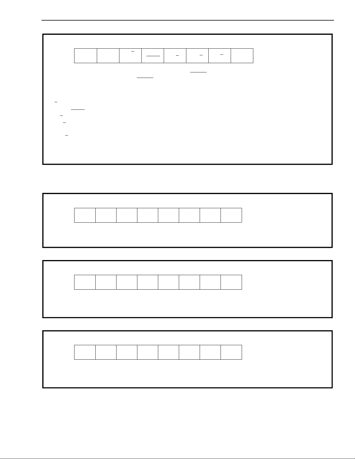
MT9092
General Control Register ADDRESS = 0Fh WRITE/READ VERIFY
Power Reset Value
000 0 00 00
RST
DATA
SEL
A/
µ
Sign -Mag/
CCITT
Rx
A/µ
MIC
A/µ
Side
A/µ
NCT
EN
76 543 2 1 0
RST Active high reset. Performs the same function as PWRST but does not affect the microport or the watchdog circuits.
DATASEL When high, the microport transmit and receive are performed on separate pins. DATA1 is receive whi le DATA2 is
A/
µ When high, A-Law (de) coding is selected. When low, µ-L aw (de)cod in g is selected .
Sign-mag/CCIT T
µ When high, the receiver driver nominal gain is set at -9.7 dB. When low this driver nominal gain is set at -12.3 dB.
RxA/
µ When high, the transmi t amp lifie r nomina l gain is se t at 15.4 dB. Whe n low this amplifi er nom inal gai n is set at 6.1
MICA/
SIDEA/
µ Wh en high, the side-ton e nominal gain is set at -18.8 dB. When low this nominal gain is set at -11 dB.
NCT EN When h igh, the new cal l tone gene rator outpu t from the DSP is selecte d as the sour ce for the lo udspeaker pa th.
To remove this reset a PWRST
transmit. When low, the microport conforms to Intel MCS-51 mode 0 specifications; DATA1 is a bi-directional
(transmit/re ceive) se rial data pin whil e DATA2 is internally di sconnecte d and tri-sta ted.
When high, sign-magnitude bit codin g is selected, When low, true CCITT PCM coding is selected.
dB.
When low, th e CODEC out put is selected fo r the loud speaker path. No te that SPKR EN must also be set high fo r
new call tone to function.
must occur or this bit must be written low.
ADDRESS 10h is RESERVED
Watchdog Register ADDRESS = 11h WRITE
Power Reset Value
---W
4
W
3
W
2
W
1
W
0
XXX0 1010
76543210
WATCHDOG RESET WORD - XXX01010
LCD Segment E nab le Reg ister 1 ADDRESS = 12h WRITE/READ VER IFY
Power Reset Value
SC
SC
8
SC
7
SC
6
SC
5
SC
4
SC
3
SC
2
1
000 0 00 00
76543210
Twelve segment control bits used for the LCD outputs. Whe n high the respective seg ment is on. When low the respective segment is
off.
LCD Segment E nab le Reg ister 2 ADDRESS = 13h WRITE/READ VER IFY
Power Reset Value
-
-
--SC
12
SC
11
SC
10
SC
9
XXXX 0000
76543210
Twelve segment control bits used for the LCD outputs. Whe n high the respective seg ment is on. When low the respective segment is
off.
Note: Bits marked "-" are reserved bits and should be written with logic "0".
7-27
Page 26
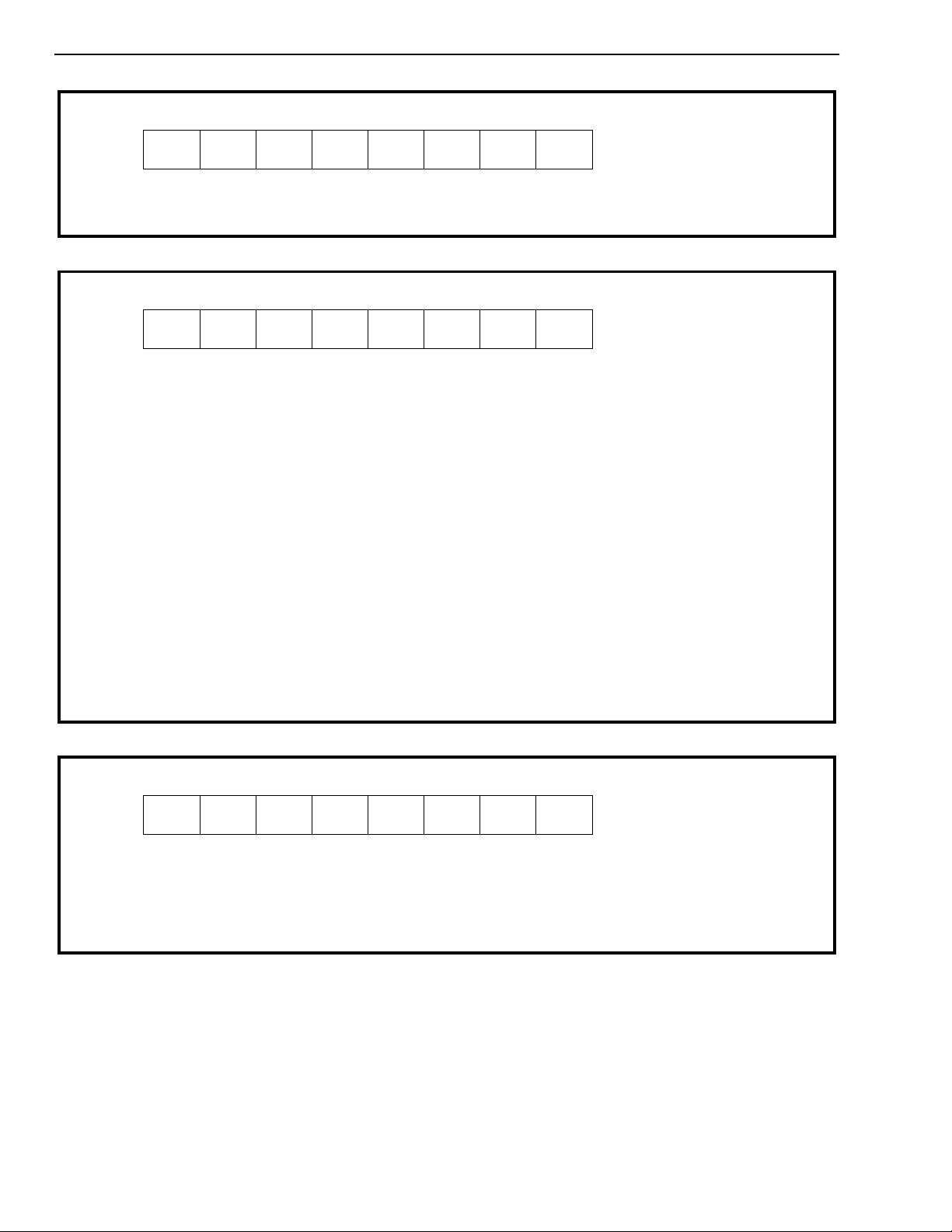
MT9092
C-Channel Register ADDRESS = 14h WRITE/READ
Power Reset Value
D
7
D
6
D
5
D
4
D
3
D
2
D
1
D
0
76543210
Micro-port access to the ST-BUS C-Channel information.
Timing Control Register ADDRESS = 15h WRITE/READ VER IFY
-- --CH
EN CH1ENCH2EN
3
CH
0
EN
76543210
All bits active high:
Ch
EN and Ch3EN
2
Channels 2 and 3 are the B1 and B2 channels, respect ivel y. PCM asso ciated with the DSP, Filter/CODEC an d trans-
ducer audio paths is conveyed in one of these channels as selected in the timing control register.
Transmit B1 and B2 data on DSTo
When high PCM from the Filter/CODEC and DSP is transmitted on DSTo in the associated channel. When low
DSTo is forced to logic 0 for the correspondi ng timeslo t. If bot h Ch
channel 2.
Receive B1 and B2 data on DSTi
When enabled PCM from DSTi is routed to the DSP and Filter/CODEC in the associated channel. If both Ch2EN
EN are enabled, data input defaults to channel 2.
and Ch
3
EN Channel 1 conveys the control/status information for the layer 1 transceiver. The full 64kb/s bandwidth is available and
Ch
1
is assigned according to which transceive r is being used. Consult the data sheets for the transceive r selected . When
high register data is transmitted on DSTo. When low this timeslot is tri-stated on DSTo. Receive C-Channel data (DSTi)
is always routed to the register regardless of this control bit's logic state.
Ch
EN Channel 0 conveys the D-Channel HDLC information. Since this function is dedicated to 16kb/s operation, only the first
0
EN and Ch3EN are enab led , da ta de faults to
2
Write = 1111 1111
Read = Not Applicabl e
Power Reset Value
XX0X 0000
Loop-back Re gi ster ADDRESS = 16h WRITE/READ VERI FY
Power Reset Value
- LBio LBoi - - ---
X00X XXXX
76543210
LB
LB
Active high enables data from the ST-BUS input to be looped back to the ST-BUS output directly at the pins. The DSTo tri-
io
state driver must also be enabled using one of the channel enable signals.
Active high enables data from ST-BUS output to be looped back to the ST-BUS input directly at the pins.
oi
ADDRES S 1 7 h-1 Ch are RESERVED
Note: Bits marked "-" are reserved bits and should be written with logic "0".
7-28
Page 27

MT9092
Receive Gain Control Register ADDRESS = 1Dh WRITE/READ VERIFY
Power Reset Value
-AUTOB5B4 B2B1B0B3
76543210
AUTO When high autonulling of the transmit PCM is enabled. When low, autonulling is disabled. This bit is used in conjunction with
the PS2 - PS0 bits of the DSP Control Register at address 1Eh.
B5-B0 Th ese 6 bits (in dica ted bel ow in hexade cim al ) are deco de d to control Rx pcm gain:
B5-B0 Gain Setting (dB) B5-B0 Gain Setting (dB)
3F +22.5 1F -25.5
3E +21.0 1E -27.0
3D +19.5 1D -28.5
3C +18.0 1C -30.0
3B +16.5 1B -31.5
3A +15.0 1A -33.0
39 +13.5 19 -34.5
38 +12.0 18 -36.0
37 +10.5 17 -37.5
36 +9.0 16 -39.0
35 +7.5 15 -40.5
34 +6.0 14 -42.0
33 +4.5 13 -43.5
32 +3.0 12 -45.0
31 +1.5 11 -46.5
30 +0.0 10 -48.0
2F -1.5 0F -49.5
2E -3.0 0E -51.0
2D -4.5 0D -52.5
2C -6.0 0C -54.0
2B -7.5 0B -55.5
2A -9.0 0A -57.0
29-10.509-58.5
28-12.008-60.0
27-13.507-61.5
26-15.006-63.0
25-16.505-64.5
24-18.004-66.0
23-19.503-67.5
22-21.002-69.0
21-22.501-70.5
20-24.000-72.0
000 0 00 00
Note: B0-B5 of addresses 20h and 21h are encoded in the same manner
Note: Bits marked "-" are reserved bits and should be written with logic "0".
7-29
Page 28
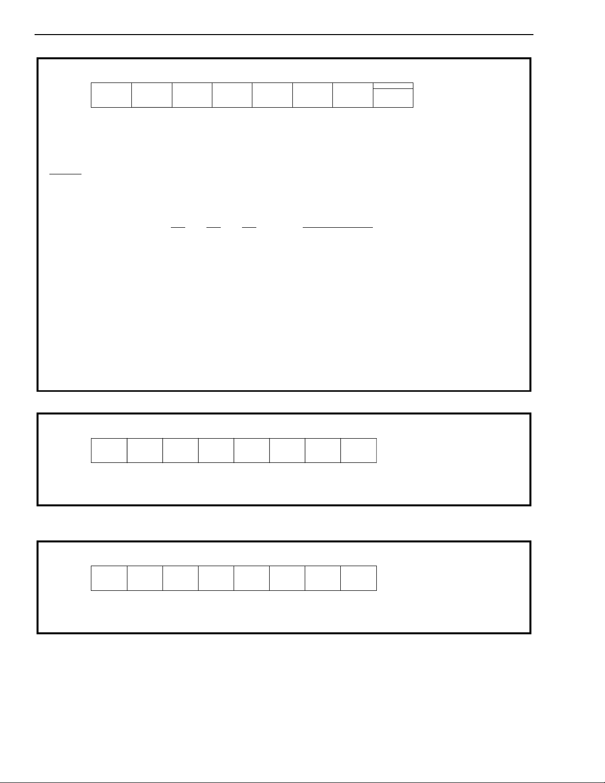
MT9092
DSP Control Register ADDRESS = 1Eh WRITE/READ VERIFY
Power Reset Value
PS2 PS1 PS0
OPT
RxMUTE -TxMUTE DRESET
76543210
OPT: When high, the tone ringer is in New Call tone mode. When low the normal tone ring er progra m is executed.
RxMUTE: This bit when high turns off the receive PCM channel, substituting quiet code.
TxMUTE: This bit when high turns off the transmit PCM channel, substituting quiet code.
DRESET
PS2-PS0: These bits are program select bits for the DSP Rom programs.
: This bit (whe n high) enables the DSP. If low, no progr ams are executed, the master cl ock is disabled and the
program counter is reset to zero.
0000 0000
PS2
0 0 0 Po wer up rese t progra m
0 0 1 Gain control program
0 1 0 DTMF & Gain control program
0 1 1 Tone Ringer & Gain control program
1 0 0 Handsfree program
101Reserved
110Reserved
111Reserved
PS1 PS0 MICRO-PROGRAM
Transmit Audio Gain Register ADDRESS = 20h WRITE/READ VERIFY
Power Reset Value
- - B5 B4 B2 B1 B0B3
XX11 0000
76543210
This register controls the transmit speech path gain in 1.5dB steps as in Receive Gain Register (address 1Dh).
Transmit DTMF Gain Register
ADDRESS = 21h WRITE/READ VERIFY
- - B5 B4 B2 B1 B0B3
76543210
This register controls the transmit DTMF level in 1.5dB steps as in Receive Gain Register (address 1Dh).
Note: Bits marked "-" are reserved bits and should be written with logic "0".
7-30
Power Reset Value
XX10 1110
ADDRESS 22h is RESERVED
Page 29
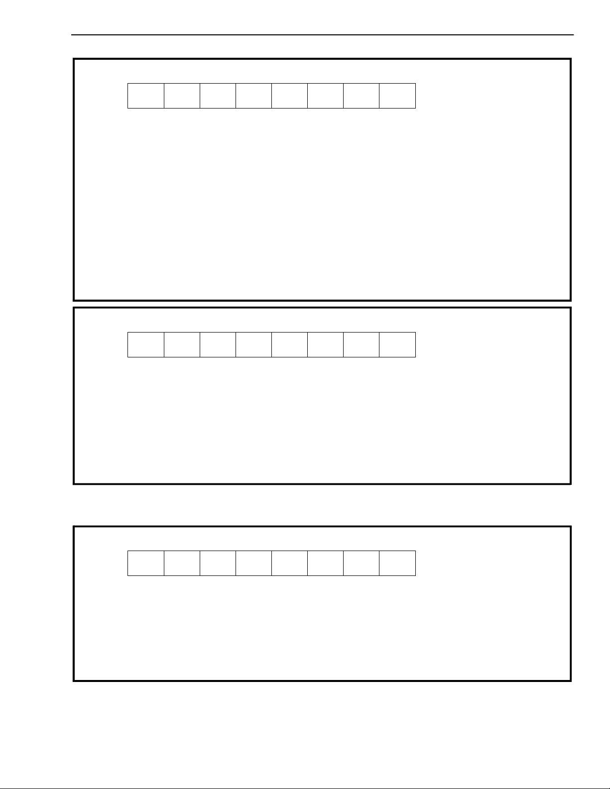
MT9092
Tone Coeff Register 1-DTM F or Tone Ringe r ADDRESS = 23h WRITE/READ VER IFY
Power Reset Value
B7 B6 B5 B4 B3 B1B2 B0
76543210
This register is used to program the low-gro up frequ enc y of the DTMF program . The tone coefficie nt is calculate d as follows:
COEF = 0.128 x Frequency
where: Frequency is in Hz (note: COEF must be converted to an 8 bit binary integer)
Highest frequency possible: 1992.2 Hz
Lowest frequency possible: 7.8 Hz
Frequenc y resolut ion: 7.8 Hz
Pre-twist: -2.1dB ± 0.2dB
This register is used to program the first frequency of the squarewave r inger prog ram. The tone coefficie nt is calculated as follow s:
COEF = 8000 / Frequency
where: Frequency is in Hz (note: COEF must be rounded off and converted to an 8 bit binary integer)
Highest frequency possible: 4000 Hz
Lowest frequency possible: 31.4 Hz
Frequenc y resolut ion : non-linear
000 0 00 00
Tone Coeff Register 2-DTM F or Tone Ringe r ADDRESS = 24h WRITE/READ VER IFY
Power Reset Value
B7 B6 B5 B4 B3 B1B2 B0
000 0 00 00
76543210
This register is used to program the high- group frequen c y of the DTMF program. The tone coefficie nt is calculated as follow s:
COEF = 0.128 x Frequency
where: Frequency is in Hz (note: COEF must be converted to an 8 bit binary integer)
Highest frequency possible: 1992.2 Hz
Lowest frequency possible: 7.8 Hz
Frequenc y resolut ion: 7.8 Hz
Pre-twist: 0dB
This register is used to program the second freque nc y of the squarewave progra m. The tone coefficien t is calculat ed simila rly to tone
ADDRESS 25h is RESERVED
Tone Ringer Warble Rate-Ton e Ringer ADDRESS = 26h WRITE/READ VER IFY
Power Reset Value
B7 B6 B5 B4 B3 B1B2 B0
000 0 00 00
76543210
The tone ringer will switch betwe en square wave frequenci es at a warble frequency defi ned by this regist er. The relationship bet wee n
the duration period of each tone and the 8 bit warble coefficient is as follows:
Tone duration (warb le freq uen cy) = 500 / COEF
where: Frequency is in Hz, and 0
Highest frequency possible: 500 Hz
Lowest frequency possible: 2.0 Hz
≤
COEF <256
Addresses: 27h to 2Dh are transmit and receive gains and coefficients used by the filters in the handsfree
decisio n circu it.
2Eh to 3Fh are scratch-pad ram locations used by the DSP algorithms as temporary storage dur-
ing calculations.
7-31
Page 30
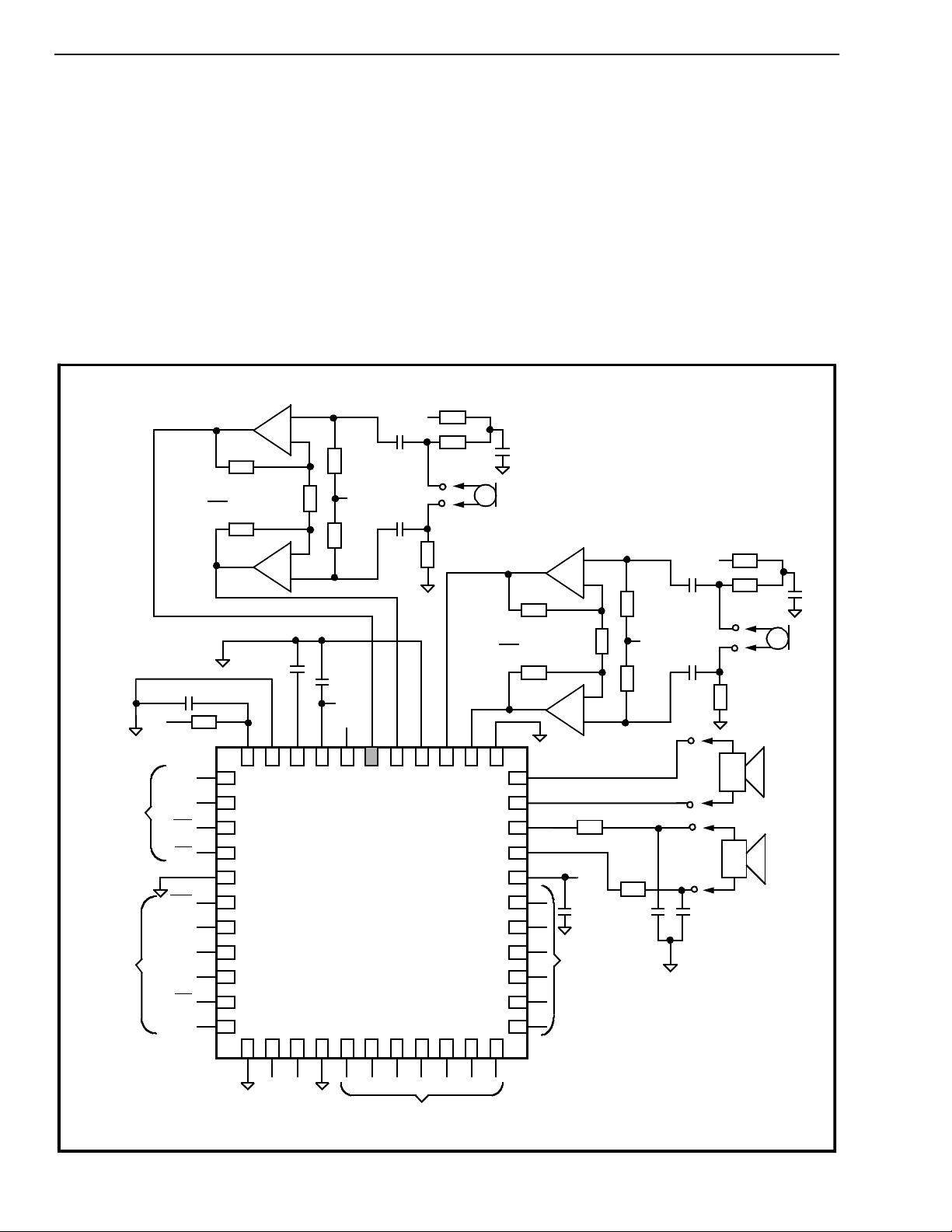
MT9092
Applications
To maintain a fully differential topology in the
transmit path the suggested connection scheme for
the transmit microphones is shown in Figure 8.
However, it is possible to use a single-ended
arrangement as shown in Figure 9 for the transmit
interface. In this case the dynamic range of the
MT9092 is reduced by half. In both figures the output
drivers are connected in a fully differential manner.
The MT9092 is a member of the Mitel family of digital
terminal equipment components. There are two
+5V
0.1µF
0.1µF
ST-BUS
Port
Transmission
Device
Serial
Microport
INTEL
MCS-51
to
+5V
DSTo
SCLK
DATA2
DATA1
Av = 1+
DSTi
C4i
F0i
IRQ
CS
WD
+
-
T
100K
VBias
100K
0.1µF
VBias
MT9092
R
2R
T
R
+
0.1µF
6 5 4 3 2 1 44 43 42 41 40
7
8
9
10
11
12
13
14
15
16
17
transmisssion devices which connect directly with
the MT9092 to complete an application; the MT8930
(SNIC) and the MT8971/72 (DSIC/DNIC). An ISDN
4-wire "TE" function is implemented with the
MT8930/MT9092 combination. A 2-wire digital phone
for PABX, key-systems and other proprietary
applications is implemented with the MT8971/72/
MT9092 combination.
Figures 10 and 11 show the 4-wire and 2-wire
applications, respectively.
330Ω
+
Electret
+
Microphone
2R
T
10µF
R
39
38
37
36
35
34
33
32
31
30
29
330Ω
+
-
T
1000pF
100K
VBias
100K
75Ω
R
+
-
75Ω
+5V
.1µF
LCD
+5V
0.1µF
0.1µF
1000pF
511Ω
Electret
Microphone
511Ω
+40Ω no m.
32Ω min.
150Ω
1000pF caps
are op t ional
511Ω
511Ω
Av = 1+
+
10µF
+
7-32
18 19 20 21 22 23 24 25 26 27 28
LCD
Note: Single-ended configurations reduce
dynamic range by a factor of two.
Figure 8 - Application Circuit - fully differential audio input
Page 31
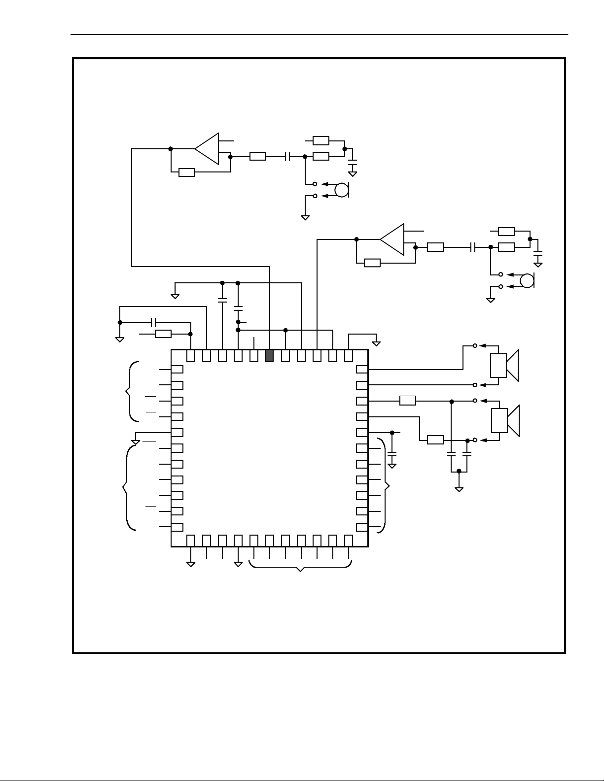
MT9092
330Ω
1µF
+5V
1K
+
VBias
–
R
T
+
10µF
Electret
+
Microphone
ST-BUS
Port
Transmission
Device
Serial
Microport
INTEL
MCS-51
to
+5V
DATA2
DATA1
DSTi
DSTo
C4i
F0i
IRQ
SCLK
CS
WD
0.1µF
6543214443424140
7
8
9
10
11
12
13
14
15
16
17
18 19 20 21 22 23 24 25 26 27 28
0.1µF
VBias
MT9092
+
–
R
39
38
37
36
35
34
33
32
LCD
31
30
29
VBias
T
75Ω
75Ω
+5V
.1µF
1000pF 1000pF
Note: Single-ended configurations reduce
dynamic range by a factor of two.
+5V
1µF
330Ω
1K
+
Electret
Microphone
40Ω nom.
+
32Ω min.
150Ω
1000pF caps
are optional
+
10µF
LCD
Figure 9 - Applica tion Circuit - single-ended audio input
7-33
Page 32
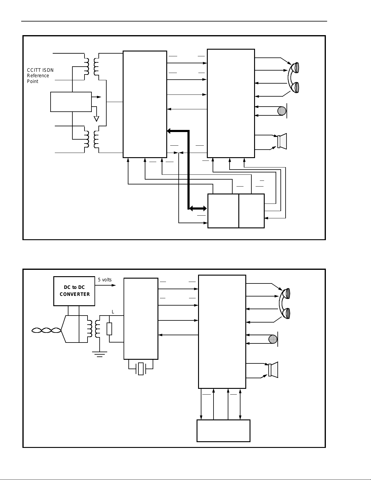
MT9092
A
A
A
A
A
A
A
A
CCITT ISDN
Reference
Point S
Interface
DC to DC
Converter
5 Volts
LTx
VBias
LRx
MT8930
SNIC
with
HDLC
Controller
(ALE) (RD
C4b
F0b
DSTo
DSTi
IRQ
)(WR)
AD0-7
C4i
F0i
DSTi
DSTo
IRQ
AD0-7
IRQ
CS
MT9092
HPhone-∏
Digital
Telephone
with
HDLC
Controller
SCLK
AS
(ALE)E(RD
8051
INTEL
DATA1
)
MCS-
51
HSPKR+
HSPKR-
M+
M-
MIC+
MIC-
SPKR+
SPKR-
R/W
(WR)
Handset
Microphone
Speaker
Twisted Pair
to Central
PBX
DC to DC
CONVERTER
Figure 10 - CCITT ISDN Voice/Data Te rminal Equipment - TE1
5 volts
Lin
Lout
Z
T
MT8972
DNIC
10.24 MHz
C4
F0
DSTo
DSTi
C4i
F0i
DSTi
DSTo
MT9092
HPhone-∏
Telephone
Controller
IRQ
Digital
with
HDLC
CSSCLK DATA1
HSPKR+
HSPKRM+
M-
MIC+
MIC-
SPKR+
SPKR-
Handset
Microphone
Speaker
INTEL
MCS-51
Figure 11 - Vo ice/Data Digital Te lephone Set Circuit
7-34
Page 33

MT9092
Programming Examples
that these steps are from the power-up reset default
definition. If some other state is currently true then
Some examples of the programming steps required
to set-up various telephony functions are given. Note
some programming steps may be omitted while new
ones may be required.
Standard Full-duplex handset call
Description Address DATA
select B-Channel of operation 15h bits 2 or 3 (as required)
reset DSP 1Eh 00h
set Rx gain (ie 0dB with Tx autonull) 1Dh 70h (or as required)
set Tx gai n (ie 0dB) 20h 30 h (or as required)
start Rx gain program 1Eh 21h
select transducers and turn on
sidetone and fi lt er /CODEC
set sidetone gain 0Bh 04h (for 0dB or as required)
optional:
set CODEC Rx and Tx gain
select A-Law ve rs us µ-Law
0Eh 99h
0Ah
0Fh
as required (0dB default)
bits 1-5 (as required)
Half-Duplex handsfree operation
Description Address DATA
select B-Channel of operation 15h bits 2 or 3 (as required)
reset DSP 1Eh 00h
set Rx gain (ie 12 dB) 1Dh 38h (or as required)
set Tx gain (ie 0dB) 20h 30 h (or as required)
start handsfre e program 1Eh 81h
select transducers and filter/CODEC
and turn off side to ne
optional:
set CODEC Rx and Tx gain
select A-Law ve rs us µ-Law
0Eh 1Eh
0Ah
0Fh
as required (0dB default)
bits 1-5 (as required)
Generate tone ringer
Description Address DATA
select B-Channel of operation 15h bits 2 or 3 (as required)
reset DSP 1Eh 00h
set Rx gain (ie 0 dB with Tx
autonull)
set Tx gai n (ie 0dB) 20h 30 h (or as required)
write tone coefficient 1 23h as required
write tone coefficient 2 24h as required
write warble tone rate coefficient 26h as required
start tone ringer program 1Eh 61h
select speake r an d fil ter/CO DE C
and turn off side to ne
1Dh 70h (or as required)
0Eh 82h
control ringer cadence by toggling
RxMUTE
1Eh 61 (on)
69 (off )
61 (on)
69 (off ) etc...
7-35
Page 34

MT9092
Generate DTMF tones
Description Address DATA
select B-Channel of operation 15h bits 2 or 3 (as required)
reset DS P 1Eh 00h
set Rx DTMF gain (ie -20 dBm0) 1Dh 22h (or as required)
set Tx audio gain (ie 0dB) 20h 30h (or as required)
set Tx DTMF gain (ie -4dBm0) 21h 2Eh (or as required)
write tone coefficient 1 23h as required
write tone coefficient 2 24h as required
start DTMF program 1Eh 41h
select transducers and filter/CODEC
(PuFC)
and turn off sidetone
optional:
set CODEC Rx gain 0Ah as required (0dB default)
send tones in only Rx or Tx by
disabling
RxMUTE or TxMUTE appropriately
0Eh as requ ired
1Eh as requ ired
New Call Tone
Description Address DATA
Assume that a B-Channel of operation has already been selected for the concurrent handset
conversation.
If this is not true select one.
select B-Channel of operation 15h bits 2 or 3 (as required)
reset DSP 1Eh 00h
**********************************************************************************
set Rx gain (ie 0 dB with Tx autonull) 1Dh 70h (or as required)
set Tx gain (ie 0dB) 20h 30h (or as required)
Note: th ese two st eps a req ui red for the con cu rr en t convers at io n only and do not aff ect new
call tone generation. See Standard Full-duplex handset call for required programming.
*********************************** ***********************************************
write tone coefficient 1 23h as required
write tone coefficient 2 24h as required
write wa rble rat e coe ff ic ient 26h as req ui re d
start new call tone ringer program 1Eh 71h
set new call tone gain 0Bh NCTG2-1 (as required)
select speaker 0Eh 0 2h
9Bh (assuming a concurrent handset
call)
enable new call tone 0Fh 01h (assuming all other bits are µ-Law
control ringer cadence by toggling
between gain control and tone ringer
with gain control programs
7-36
1Eh 71h (on)
31h (off)
71h (on) etc...
Page 35
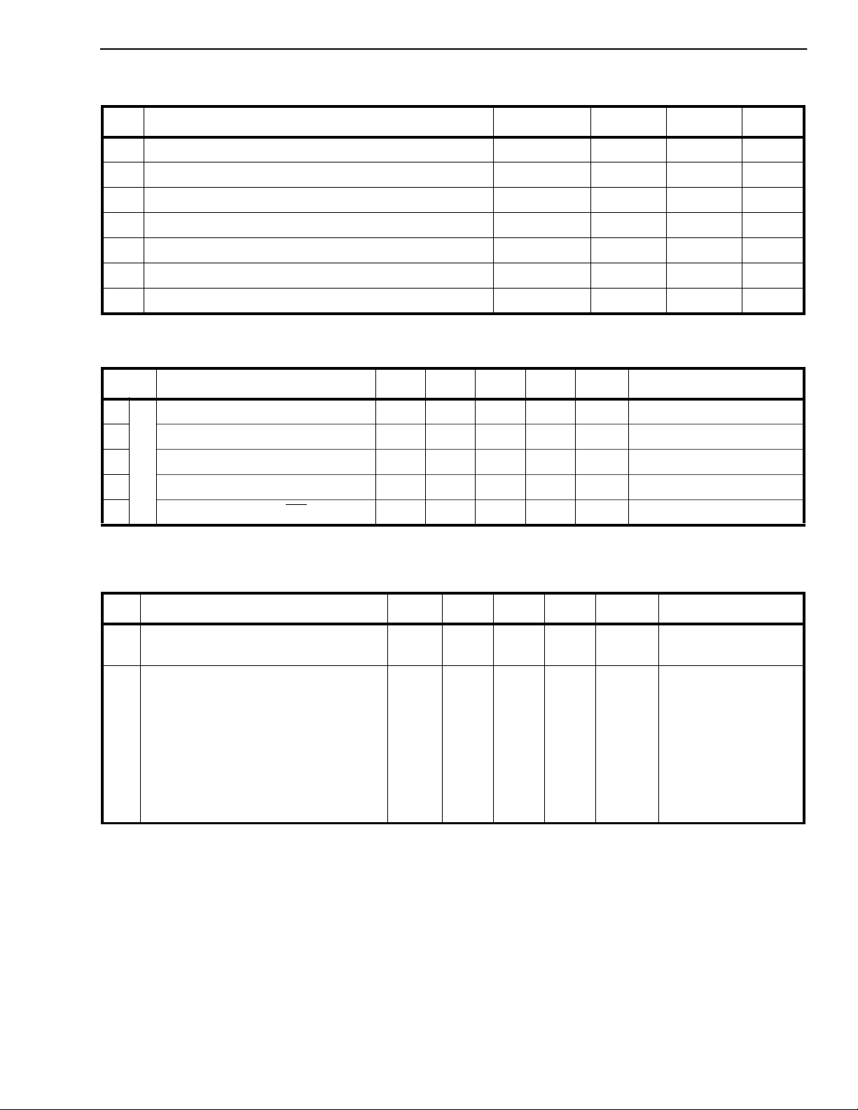
Absolute Maximum Ratings
Parameter Symbol Min Max Units
MT9092
1 Supply Voltage V
DD-VSS
2 Voltage on any I/O pin V
3 Cu r rent on any I/O pin (transducers excluded) I
4 St orage Temperature T
5 Pow e r Dissipation (package ) Plastic P
I/VO
I/IO
S
D
-0.3 7 V
VSS-0.3 VDD+0.3 V
±20 m A
-65 +15 0 °C
750 mW
6 St atic Discharge ESD ±2.0 KV
7 L atch-up Current I
LU
Recommended Operating Conditions - Voltages are with respect to V
SS
±100 mA
unless otherwise stated.
Characteris tics Sym Min Typ Max Units Test Conditions
1 Supply Voltage V
2 Input Voltage (high) * V
3 Input Voltage (low) * V
4 Operating Temperat ure T
5 Clock Frequenecy (C4i
* Excluding PWRST
which is a Schmitt Trigger Input.
)f
CLK
4.75 5 5.25 V
DD
2.4 V
IH
V
IL
A
SS
-40 + 85 °C
4092 4096 4100 kHz
DD
V Noise margin = 400mV
0.4 V Noise margin = 400mV
Power Characteristics
Characteristics Sym Min Typ Max U n its Test Conditio ns
1 Supply Current (clock enabled, all
functions off
2 Supply Current by function
Filter/Codec
HDLC
DSP
Handset Driver (bias only, no signal)
Speaker Driver (bias only, no signal)
Timing Control, C-Channel, ST-BUS,
etc.
Total all functio ns ena bled
Note 1: P ower delivered to the load is in addition to the bias current requirements.
Note 2: I
is not ad di tiv e to I
DDFT
DDC1
.
I
DDC1
I
DDF1
I
DDF2
I
DDF3
I
DDF4
I
DDF5
I
DDF6
I
DDFT
1.5
1.0
1.5
1.5
1.5
1.0
8.0 14
6mA
mA
mA
mA
mA
mA
See Note 1.
See Note 1.
mA
mA
See Note 2.
7-37
Page 36
MT9092
DC Electrical Characteristics
otherwise stated.
Characteristi cs Sym Min Typ
1 Input HIGH Voltage TTL inp uts V
2 Input LOW Voltage TTL inputs V
3 VBias Voltage Output V
4 Input Leakage Current
5 Positive Going Threshold
Voltage (PWRST
Negative Going Threshold
Voltage (PWRST
6 Output HI GH Current TTL O/P I
7 Output L O W Cu rre nt TT L O/P I
8 Output Voltage V
9 Output Leakage Curren t
10 Output Capa citance C
11 Input Capacitan ce C
† DC Electrical Characteristics are over recommended temperature and range & recommended power supply voltages.
‡ Typical figures are at 25°C and are for design aid only: not guaranteed and not subje ct to producti on testing.
1 TTL compatible pins only.
1
only)
only)
†
(except LCD Drive Pins) - Voltages are with respect to ground (V
‡
Max Units Test Conditions
2.0 V
IN
IL
Bias
I
IZ
V
V
OH
OL
Ref
1
I
OZ
3.3 1.5
T+
T-
-10 -16 m A VOH = 2.4V DSTo, WD,
510 mAV
o
i
VDD/2 V Max. Load = 10kΩ
0.1 10 µAVIN = VDD to V
(VDD/2)
-1.5
0.01 10 µAV
15 pF
10 pF
0.8 V
= 0.4V DSTo, WD,
OL
V No load
= VDD and V
OUT
) unless
SS
SS
DATA1,
DATA2, IRQ
DATA1,
DATA2, IRQ
SS
DC Electrical Characteristics† - LCD Drive Pins - Voltages are with respect to ground (V
stated.
Characteris tics Sym Min Typ Max Units Test Con di tions
1 Output High Voltage Both
Segment and Backplane
2 Output Low Voltage Both
Segment and Backplane
3 Segment Output Load --- --- 1200 pF
4 Backplane Output Load --- --- 7200 pF
5 Frequency 62 62.5 63 Hz
V
OH
V
OL
4.8 --- --- Volts Io = 1mA, V
--- --- 0.2 Volts Io = 1m A, VDD = 5V
) unless otherwise
SS
= 5V
DD
7-38
Page 37
MT9092
AC Characteristics† for A/D (Transmit) Path - 0dBm0 = 1.421V
CODEC. (V
and transmit idle channel noise.
1 Analog input equivalent to
2 Absolute half -ch annel gain.
3 Gain tracking vs. input level
4 Signal to total Distortion vs.
= 0.5 volts and V
Ref
= 2.5 volts). All parameters pertain exclusively to the Filter/CODEC except absolute half-channel gain
Bias
Characteristics Sym Min Typ
overload decision
Transmit filter gain = 0dB setting
All other transmit filter settings
(1 to 7dB) are in addition to 0dB
setting
CCITT G.714 Method 2
input level.
CCITT G.714 Method 2
A
A
G
G
G
G
G
D
Li3.17
Li3.14
AX1
AX2
AX1
AX2
TX
QX
5.4
14.7
-0.15
-0.15
-0.3
-0.6
-1.6
35
29
24
5.79
6.0
6.1
15.4
‡
Max Units Test Conditions
6.8
16.1
+0.15
+0.15
0.3
0.6
1.6
for µ-Law and 1.477V
rms
Vp-p
Vp-p
dB
dB
dB
dB
dB
dB
dB
dB
dB
dB
for A-Law, at the
rms
µ-Law
A-Law
Both at CODEC
MICA/u=0*
MICA/u
=1*
MIC± or M± to PCM
1020Hz
MICA/u=0*
MICA/u
=1*
from nominal
MIC± or M± to PCM
1020Hz
3 to -40 dBm0
-40 to -50 dBm0
-50 to -55 dBm0
0 to -30dBm0
-40 dBm0
-45 dBm0
5 Transmit Idle Channel Noise N
6 Gain relat ive to gain at 102 0Hz
<50 Hz
60 Hz
200 Hz
300-3000 Hz
3000-3400 Hz
4000 Hz
>4600 Hz
7 Absolute Delay D
CX
N
PX
G
RX
-0.25
-0.9
AX
15
-72
17.5
-66
-25
-30
0.0
0.25
0.25
-12.5
-25
dBrnC0
dBrn0p
dB
dB
dB
dB
dB
dB
dB
µ-Law
A-Law
360 µs at frequency of minimum
delay
8 Group Delay relative to D
AX
D
DX
9 Power Supply Reject ion
f=1020 Hz
f=0.3 to 3 kHz
f=3 to 4 kHz
f=4 to 50 kHz
† AC Electrical Characteristics are over recommended temperature range & recommended power supply voltages.
‡ Typical figures are at 25°C and are for design aid only: not guaran teed and not subje ct to producti on testing.
* Note: MICA/u
, refer to General Control Register, address 0Fh.
PSS R
PSSR1
PSSR2
PSSR3
37
40
35
40
750
380
130
750
µs
µs
µs
µs
dB
dB
dB
dB
500-600 Hz
600-1000 Hz
1000-2600 Hz
2600 - 2800 Hz
±1000mV
µ-Law
PSSR1-3 not production
tested
peak signal
rms
7-39
Page 38
MT9092
AC Characteristics† for D/A (Receive) Path - 0dBm0 = 1.421V
CODEC. (V
idle channel noise.
1 Analog output at the CODEC full
scale
2 Absol ute hal f-channe l gain.
Receive filter gain = 0dB setting
= 0.5volts and V
Ref
= 2.5 volts). All parameters pertain exclusively to the Filter/CODEC except absolute gain and receive
Bias
Characteristics Sym Min Typ
A
Lo3.17
A
Lo3.14
G
AR1
G
AR2
G
AR3
-0.6
-12.9
-10.3
‡
5.704
5.906
0.2
-12.3
-9.7
for µ-Law and 1.477V
rms
Max Units Test Conditions
0.95
-11.8
-9.1
Vp-p
Vp-p
dB
dB
dB
µ-Law
A-Law
PCM to SPK R±
PCM to HS PK R ± , RxA /u
PCM to HS PK R ± , RxA /u
1020Hz
All other receive filter settings
(-1 to -7dB) are in addition to
0dB set tin g
G
AR1
G
AR2
G
AR3
-0.15
-0.15
-0.15
+0.15
+0.15
+0.15
dB
dB
dB
PCM to SPK R±
PCM to HS PK R ± , RxA /u
PCM to HS PK R ± , RxA /u
from nominal
1020Hz
3 G ain tra cking vs. input level
CCITT G.714 Met hod 2
G
TR
-0.3
-0.6
-1.6
4 Signal to total distortion vs. input
level.
CCITT G.714 Met hod 2
5 Receive Idle Channel Noise N
6 G ain relat ive to gain at 1020Hz
G
QR
35
29
24
CR
N
PR
G
RR
200 Hz
300-3000 Hz
3000-3400 Hz
-0.25
-0.90
4000 Hz
>4600 Hz
7 Absol ute Dela y D
8 G roup Delay relat ive to D
AR
AR
D
DR
240 µs at frequency of min. delay
750
380
130
750
9 Crosstalk D/A to A/D
A/D to D/A
† AC Electrical Characteristics are over recommended temperature range & recommended power supply voltages.
‡ Typical figures are at 25°C and are for design aid only: not guaranteed and not subje ct to producti on testing.
* Note: RxA/u
, refer to General Control Register, address 0Fh.
CT
CT
RT
TR
0.3
0.6
1.6
15.5
-75
0.25
0.25
0.25
-12.5
-25
-74
-80
dB
dB
dB
dB
dB
dB
dBrnC0
dBrn0p
dB
dB
dB
dB
dB
µs
µs
µs
µs
dB
dB
3 to -40 dBm0
-40 to -50 dBm0
-50 to -55 dBm0
0 to -30dBm0
-40 dBm0
-45 dBm0
µ-Law
A-Law
500-600 Hz
600-1000 Hz
1000-2600 Hz
2600 - 2800 Hz
G.714.16
for A-Law, at the
rms
=0*
=1*
=0*
=1*
AC Electrical Characteristics† for Side-tone Path
-16.7
-12.6
‡
Max Uni t s Test Conditions
-16.2
-12.1
dBdBSIDEA/u , MICA/u, RxA/u all 0
SIDEA/u
, MICA/u, RxA/u all 1
M± inputs to HSPKR± outputs
1000Hz
+0.3
+0.3
dBdBSIDEA/u =0
SIDEA/u
=1
from nominal
relative measurements w.r.t.
G
& G
AS1
AS2
Characteristi cs Sym Min Typ
1 Absolute path gain
Gain adjust = 0dB
All other settings
(-9.96 to +9.96dB)
† AC Electrical Characteristics are over recommended temperature range & recommended power supply voltages.
‡ Typical figures are at 25°C and are for design aid only: not guaranteed and not subje ct to producti on testing.
7-40
G
AS1
G
AS2
G
AS
G
AS
-17.2
-13.1
-0.3
-0.3
Page 39
AC Electrical Characteristics† for New Call Tone
Characteristics Sym Typ
MT9092
‡
Units Test Conditions
1 New Call Tone Output voltage
(SPKR+ to SPKR -)
V
V
V
V
NCT1
NCT2
NCT3
NCT4
6.0
2.390
0.950
0.380
Vp-p
Vp-p
Vp-p
Vp-p
NCTG0=0, NCTG1=0
NCTG0=1, NCTG1=0
NCTG0=0, NCTG1=1
NCTG0=1, NCTG1=1
load > 34 ohms across SPK R±
† AC Electrical Characteristics are over recommended temperature range & recommended power supply voltages.
‡ Typical figures are at 25°C and are for design aid only: not guaran teed and not subje ct to producti on testing.
Electrical Characteristics† for Analog Outp uts
Characteristics Sym Min Typ‡Max Units Test Conditions
1 Earpiece load impedance E
2 Allowa ble E arpiece capacit ive
E
load
3 Earpiece harm onic dist ortio n E
4 Speaker load im pedance S
5 Allowa ble S peaker capacitive
S
load
ZL
CL
ZL
CL
260 300 ohms across HSPKR±
300 pF each pin: HSPKR+
D
0.5 % 300 ohms load across
HSPKR± (to l-15%),
V
o
Rx gain=0dB
34 40 ohms a cross SPKR±
300 pF each pin SPKR+
≤6.2Vp-p,Rx A/u=1,
HSPKR-
SPKR-
6 Speaker harm onic distort ion S
D
0.5 % 40 ohms load across SPKR±
(tol-15%),
V
≤6.2Vp-p, R x gain=0dB
O
† Electri cal Cha racte risti cs are over recom men ded temperatu re ran ge & recomm ende d power supply voltages.
‡ Typical figures are at 25°C and are for design aid only: not guaran teed and not subje ct to producti on testing.
Electrical Characteristics† for Analog Inputs
Characteristics Sym Min Typ‡Max Uni ts Test Conditio ns
1 Diff erent ial input volta ge with out
V
ID
overloading CODEC
2 Input impedance Z
† Electri cal Cha racte risti cs are over recom men ded temperatu re ran ge & recomm ende d power supply voltages.
‡ Typical figures are at 25°C and are for design aid only: not guaran teed and not subje ct to producti on testing.
50 kΩ M IC+ , MIC-, M + or M-
I
2.87
1.02
Vp-p
Vp-p
MICA/u =0, A/u=0
MICA/u
=0, A/u=1
across MIC± or M ± i nputs,
Tx filter gain = 0dB sett ing
to V
.
SS
7-41
Page 40
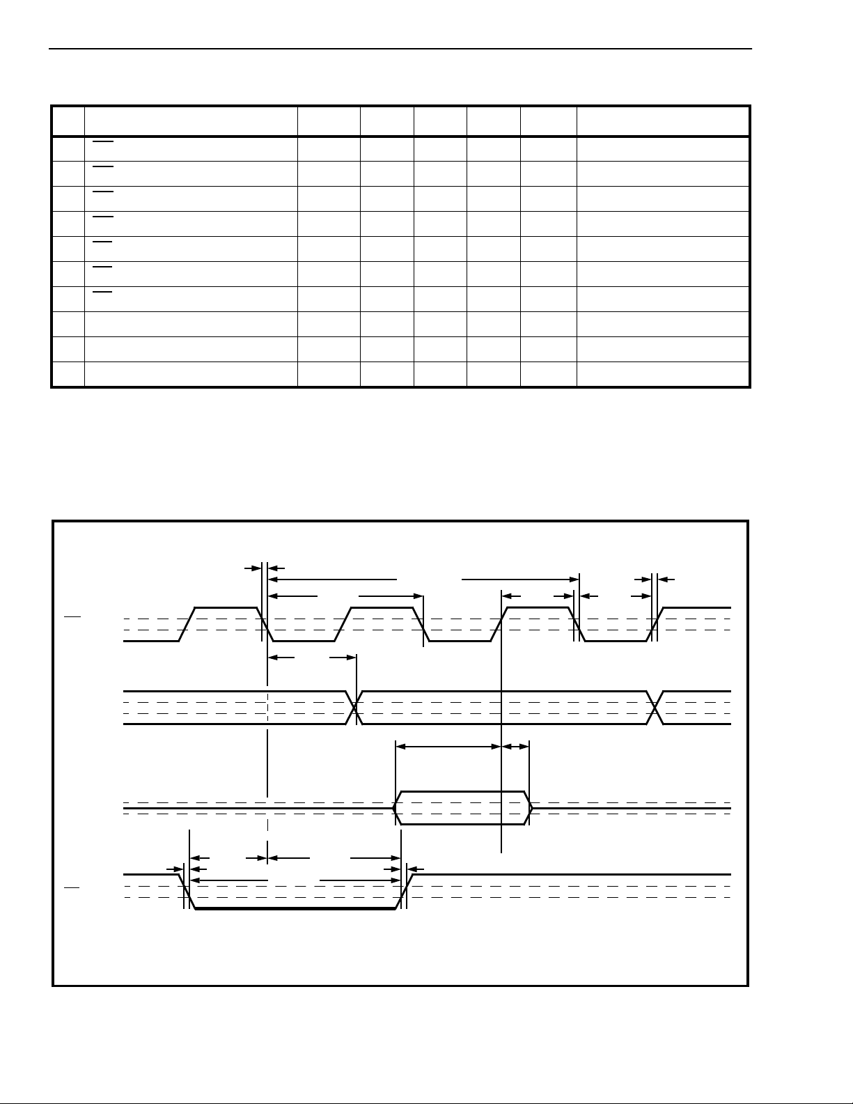
MT9092
AC Electrical Characteristics† - ST-BUS Timing (See Figure 12)
Characteristics Sym Min Typ
‡
Max Units Test Conditions
1C4i
2C4i
3C4i
4C4i
5F0i
6F0i
7F0i
8 DSTo Delay t
9 DSTi Setup Time t
10 DSTi Hold Time t
† Timing is over recommended temperature range & recommended power supply voltages.
‡ Typical figures are at 25°C and are for design aid only: not guaranteed and not subje ct to producti on testing.
Clock Period t
Clock High Period t
Clock Low Period t
Clock Transition Time t
Frame Pulse Setup Time t
Frame Pulse Hold Time t
Frame Pulse Width Low t
C4P
C4H
C4L
T
F0iS
F0iH
F0iW
DSToD
DSTiS
DSTiH
243 244 245 ns
121 122 123 ns
121 122 123 ns
20 50 ns
50 ns
50 ns
150 ns
100 125 ns CL=50 pF
30 ns
50 ns
C4i
DSTo
DSTi
F0i
2.4V
0.4V
2.4V
0.4V
2.4V
0.4V
2.4V
0.4V
t
t
T
t
C4P
t
DSToD
t
T
t
F0iS
t
F0iW
t
F0iH
1 bit cell
t
T
t
DSTiS
t
DSTiH
t
C4H
t
C4L
T
7-42
Figure 1 2 -ST-BUS Timing Diagram
Page 41
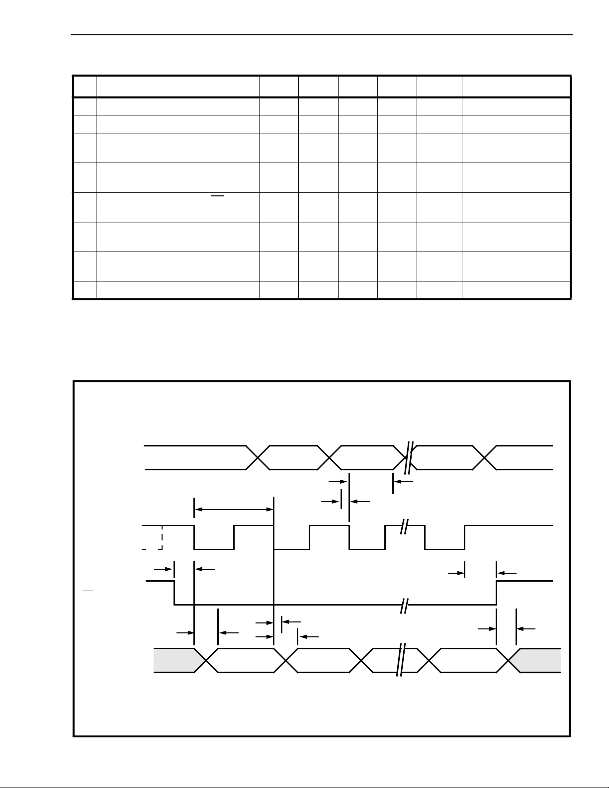
AC Electrical Characteristics† - Microport Timing (see Figure 13)
Characteristi cs Sym Min Typ
1 Receive data setup A 10 n s
2 Receive data hold B 10 ns
‡
Max Units Test Condition s
MT9092
3 Transmit data delay from clock
C80ns50 pF
falling edge
4 High Z to valid data from SCLK
D80ns50 pF
falling edge
5 Valid data to high Z from CS
rising
E80ns50 pF
edge
6 Current transmit data hold
F0ns
from clock falling edge
7 Chip Select t o SCLK setup and
G0 ns
hold times
8 SCLK clock period (3 MHz) H 333 ns
† Timing is over recommended temperature range & recommended power supply voltages.
‡ Typical figures are at 25°C and are for design aid only: not guaran teed and not subje ct to producti on testing.
DATA 1
RECEIVE
SCLK
CS
DATA 1 or DATA 2
TRANSMIT
012 7
H
G
D
01267
B
A
F
C
G
E
Figure 1 3 - Serial Microport Timing Diagram
7-43
Page 42

MT9092
NOTE S:
7-44
 Loading...