

Page 1
MT91610
Analog Ringing SLIC
Preliminary Information
Features
• Transformerless 2W to 4W conversion
• Controls battery feed to line
• Programmable line impedance
• Programmable network balance impedance
• Off-hook and dial pulse detection
• Protects against GND short circuit
• Programmable gain
• Programmable constant current mode with
constant voltage fold over
• Transformerless balanced ringing with
automatic ring trip circuit. No mechanical relay
• Supports low voltage ringing
• Line polarity reversal
• On-hook transmission
• Power down and wake up capability
• Meter pulse injection
• Ground Key detection
Applications
Line interface for:
• PABX
• Intercoms
• Key Telephone Systems
• Control Systems
DS5181 ISSUE 2 February 2000
Package Information
MT91610AQ 36 Pin QSOP Package
-40°C to +85°C
Description
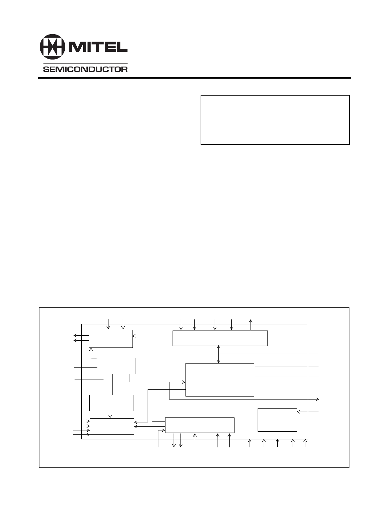
The Mitel MT91610, with an external bipolar driver
(Figure 4), provides an interface between a switching
system and a subscriber loop. The functions
provided by the MT91610 include battery feed,
programmable constant current with constant voltage
fold over for long loop, 2W to 4W conversion, offhook and dial pulse detection, direct balance ringing
with built in ring tripping, unbalance detection, user
definable line and network balance impedance’s and
gain, and power down and wake up. The device is
fabricated as a CMOS circuit in a 36 pin QSOP
package.
TD
RD
TIP
RING
RF1, RF2
RC
CP4
CP6
CP7
RV
PD
Tip/Ring Drive
Controller
Line Sense
Over-Current
Protection Circuit
Ring Drive
Controller
GTX1 GTX0 VX
Loop Supervision
UD
SHK
VREF
ESIESE
Audio Gain & Network
Balance Circuit
2 W to 4 W
Conversion & Line
Impedance
CP3
CP1
CP2
Figure 1 - Functional Block Diagram
DCRI
Line
Reverse
Driver
VDD
GND
VEE
VR
Z3
Z2
CP5
LR
VBAT
1
Page 2
MT91610 Preliminary Information
VDD
VREF
RING
RF1
CP1
CP2
CP3
CP4
ESE
DCRI
TD
TF1
NC
TIP
LR
NC
RD
PD
1
2
3
4
5
6
7
8
9
10
11
12
13
14
15
16
17
18
36
35
34
33
32
31
30
29
28
27
26
25
24
23
22
21
20
19
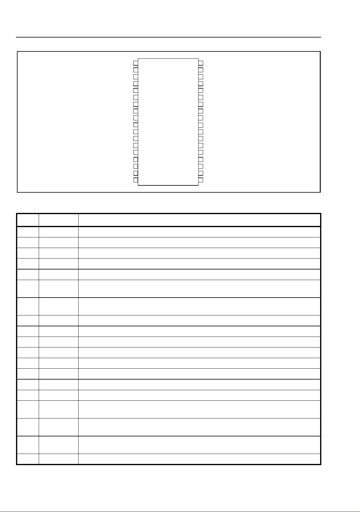
Figure 2 - Pin Connections
Pin Description
Pin # Name Description
1 VDD Positive supply rail, +5V.
VEE
RV
CP7
SHK
VBAT
UD
RC
CP6
VR
GTX1
ESI
VX
GTX0
Z3
Z2
CP5
Z1
AGND
2TDTip Drive (Output). Controls the Tip transistor. Connects 150nF cap to GND.
3 TF1 Tip Feed 1 (Output). Connects to the Tip transistor and to TIP via the Tip feed resistor.
4NCNo Connection Left open
5 Tip Tip. Connects to the TIP lead of the telephone line.
6 VREF Reference Voltage (Input). Used to set the subscribers loop constant current. A 0.1uF
cap should be connected between this pin and GND for noise decoupling.
7LRLine Reverse (Input). This pin should be set to 0V for NORMAL polarity. Setting the pin
to +5V reverses the polarity of Tip and Ring
8 Ring Ring. Connects to the RING lead of the telephone line
9 RF1 Ring Feed 1 (Output). Connects to the RING lead via the Ring feed resistor
10 NC No Connection Left open
11 RD Ring Drive (Output). Controls the Ring transistor. Connects 150nF cap to GND.
12 CP1 CP1. A 220nF capacitor should be connected between this pin and pin 13
13 CP2 CP2. A 330nF capacitor for loop stability is connected between this pin and pin 14
14 CP3 CP3. A 330nF capacitor for loop stability is connected between this pin and pin 13
15 CP4 CP4. A 100nF cap should be connected between this pin and GND
16 ESE External Signal Enable (Input). A logic ’1’ enable the MPI (Meter Pulse Input) to Tip /
Ring. This pin should be set to logic ’0’ when not used.
17 PD Power Do wn (Input). A logic ’1’ pow er down the de vice . This pin should be set to logic ’0’
for normal operation.
18 DCRI DC voltage for Ringing Input (Input) The positive voltage supply for balance ringing.
The input DC voltage range is from 0V to +72V.
19 AGND Analog Ground. 4 Wire Ground, normally connected to system ground.
2
Page 3

Preliminary Information MT91610
Pin Description (continued)
Pin # Name Description
20 Z1 Line Impedance Node 1. A resistor of scaled value "k" is connected between Z1 and Z2.
This connection can not be left open circuit.
21 CP5 Line Impedance AC couple. A 0.1uF cap must be connected between this pin and Z1
(pin 16)
22 Z2 Line Impedance Node 2. This is the common connection node between Z1 and Z3.
23 Z3 Line Impedance Node 3. A network either resistive or complex of scaled value "k" is
connected between Z3 and Z2. This connection can not be left open circuit.
24 GTX0 Gain Node 0. This is the common node between Z3 and VX where resistors are
connected to set the 2W to 4W gain.
25 VX Transmit Audio. 4W analog signal from the SLIC.
26 ESI External Signal Input. 12 / 16 KHz signal input
27 GTX1 Gain Node 1. The common node between VR and the audio input from the CODEC or
switching network where resistors are fitted to sets the 4W to 2W gain
28 VR Receive Audio. 4W analog signal to the SLIC.
29 CP6 Ringing Cap. A 0.47uF cap should be connected between this pin and GND for ringing
voltage filtering.
30 RC Ringing Control. An active high (+5V) on this pin will set up the DC feed and gain of the
SLIC to apply 20 Hz ringing. When low (0V) set the SLIC in normal constant current mode
of operation.
31 UD UnBalance Detect. To indicate an offset current between Tip and Ring
32 VBAT VBAT. The negative battery supply, typically at -48V
33 SHK Switch Hook. This pin indicates the line state of the subscribers telephone. The output
can also be used for dial pulse monitoring. This pin is active high
34 CP7 Deglitching Cap. A 33nF should be connected between this pin and GND
35 RV Ringing Voltage. 20 Hz sinusoidal or square wave AC in for balance ringing
36 VEE Negative supply rail, -5V.
Functional Description
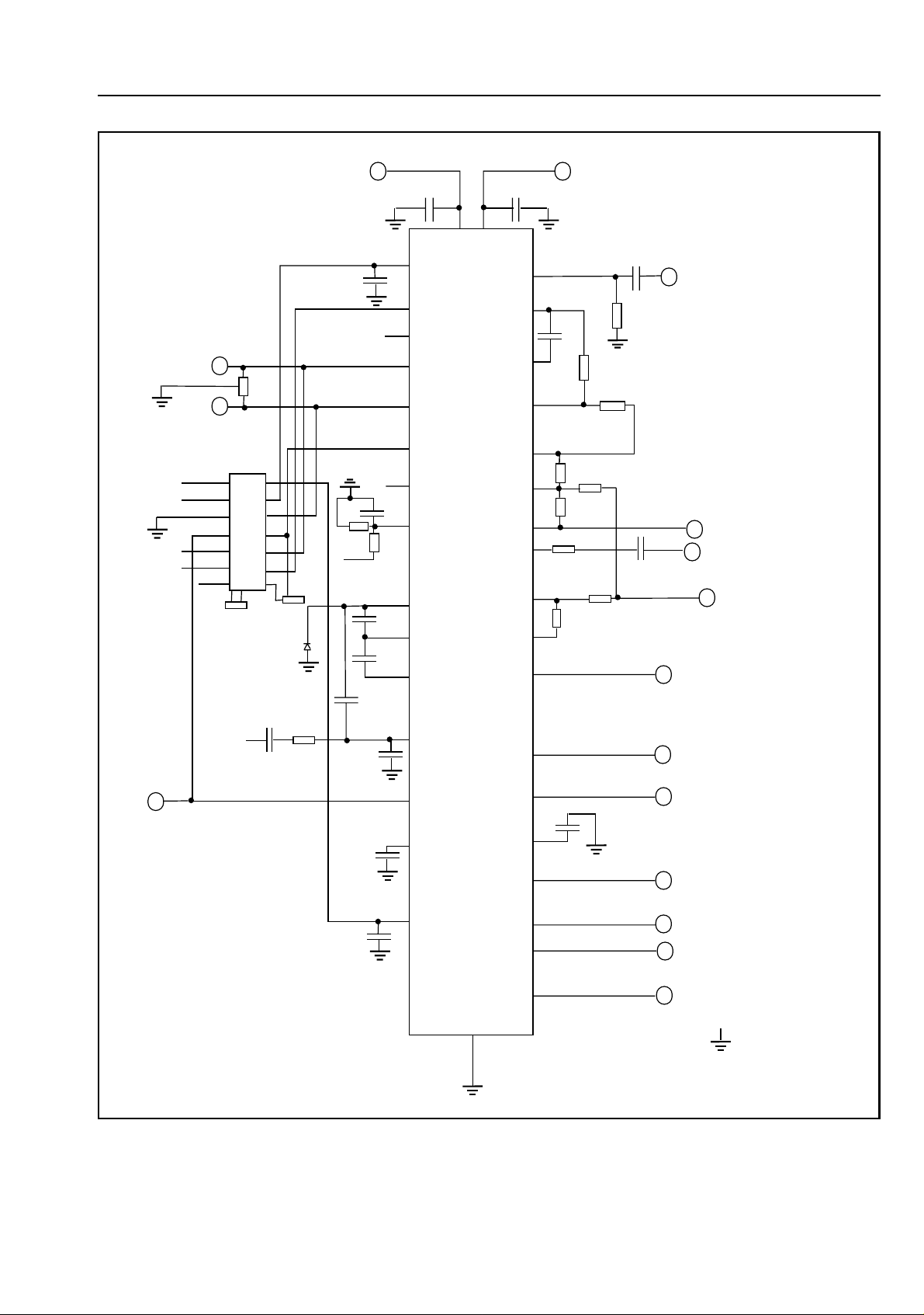
Refer to Figure 4 for MT91610 components
designation.
The MT91610, with external bipolar transistors,
functions as an Analog Line SLIC for use in a 4 Wire
switched system. The SLIC performs all of the
BORSH functions whilst interfacing to a CODEC or
switching system.
2 Wire to 4 Wire conversion
The SLIC performs 2 wire to 4 wire conversion by
taking the 4 wire signal from an analog switch or
voice CODEC, and converting it to a 2 wire
differential signal at Tip and Ring. The 2 wire signal
applied to tip and ring by the phone is converted to a
4 wire signal, which is the output from the SLIC to
the analog switch or voice CODEC.
Gain Control
It is possible to set the Transmit and Receive gains
by the selection of the appropriate external
components.
The gains can be calculated by the following
formulae:
2W to 4W gain
Gain 2 - 4 = 20 Log [ R8 / R7]
4W to 2W gain
Gain 4 - 2 = 20 Log [0.891 * [R10 / R9)]
3
Page 4
MT91610 Preliminary Information
Impedance Programming
The MT91610 allows the designer to set the device’s
impedance across TIP and RING, (ZTR), and
network balance impedance, (ZNB), separately with
external low cost components.
The impedance (ZTR) is set by R4, R5, whilst the
network balance, (ZNB), is set by R6, R8, (see Figure
4.)
The network balance impedance should be
calculated once the 2W - 4W gain has been set.
Line Impedance
For optimum performance, the characteristic
impedance of the line, (Zo), and the device’s
impedance across TIP and RING, (ZTR), should
match. Therefore:
Zo = Z
TR
The relationship between Zo and the components
that set ZTR is given by the for mula:
Loop Supervision
The Loop Supervision circuit monitors the state of
the phone line and when the phone goes "Off Hook"
the SHK pin goes high to indicate this state. This pin
reverts to a low state when the phone goes back "On
Hook" or if the loop resistance is too high (>2.3KΩ)
When loop disconnect dialing is being used, SHK
pulses to logic 0 indicate the digits being dialled.
This output should be debounced.
Constant Current Control & Voltage
Fold Over Mode
The SLIC employs a feedback circuit to supply a
constant feed current to the line. This design is
accomplished by sensing the sum of the voltages
across the feed resistors, Ra and Rb, and comparing
it to the input reference voltage, Vref, that
determines the constant current feed current.
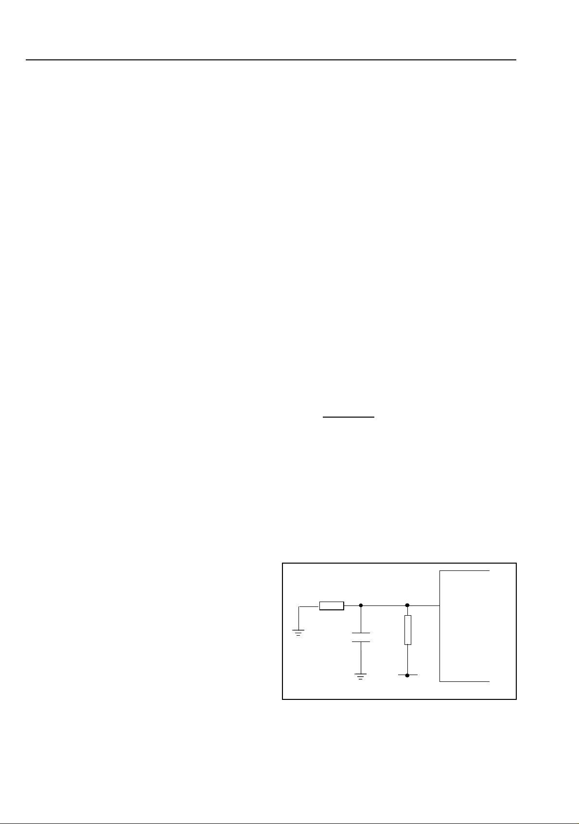
By using a resistive divider network, (Figure 3), it is
possible to generate the required voltage to set the
I
. This voltage can be calculated by the formula:
LOOP
Zo / ( Ra+Rb) = kZo / R4
where kZo = R5
Ra = Rb
The value of k can be set by the designer to be any
value between 20 and 250. R4 and R5 should be
greater than 50kΩ.
Network Balance Impedance
The network balance impedance, (ZNB), will set the
transhybrid loss performance for the circuit. The
transhybrid loss of the circuit depends on both the 4 2 Wire gain and the 2 - 4 Wire gain.
The method of setting the values for R6 (or Z6... it
can be a complex impedance) is given as below:
R6 = R7 * (R9 / R10) * 2.2446689 * ( ZNB / ZNB + Zo)
Please note that in the case of Zo not equal to Z
(the THL compromized case) R6 is a complex
impedance. In the general case of Zo matches to Z
(the THL optimized case) R6 is just a single resistor.
NB
NB
I
= [ G * 5] * 3
LOOP
(Ra +Rb)
where, G = R2 / (R1 + R2)
I
is in Ampere.
LOOP
R1= 200KΩ
From Figure 3 with Ra = Rb = 100 Ω
For I
For I
For I
= 20mA, R2 = 72.73 KΩ
LOOP
= 25mA, R2 = 100 KΩ
LOOP
= 30mA, R2 = 133.33 KΩ
LOOP
R2
**kΩ
C2
0.1uF
** See Figure 6
R1
200K
+5V
6
V
REF
MT91610
Figure 3 - Loop Setting
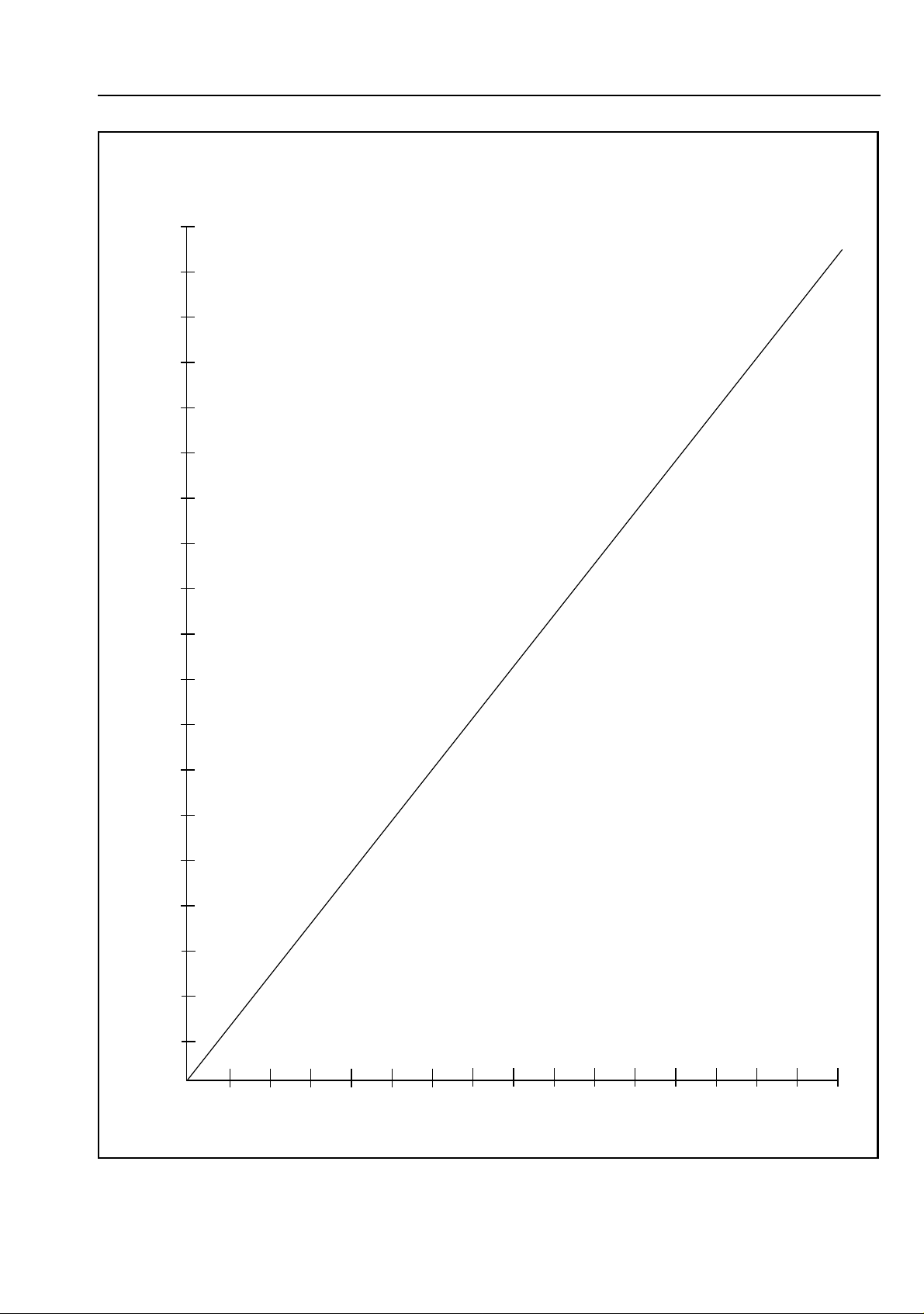
For convenience, a graph which plots the value of
R2 (KΩ) versus the expected loop current is shown
in Figure 6.
4
Page 5

Preliminary Information MT91610
As +5V is used as the reference voltage to generate
the loop current, any noise on the +5V rail will
deteriorate the PSR (Power Supply Rejection)
parameter of the SLIC. It is therefore impor tant to
decouple +5V to GND. A 0.1uF cap at Vref pin (pin6)
is recommended.
The MT91610 operating current mode is
recommended to be between 20mA and 30mA. The
device will automatically switch to voltage hold over
mode should an unexpected long loop situation
occur for a given programmed loop current. The
lowest operational current should be 16mA with
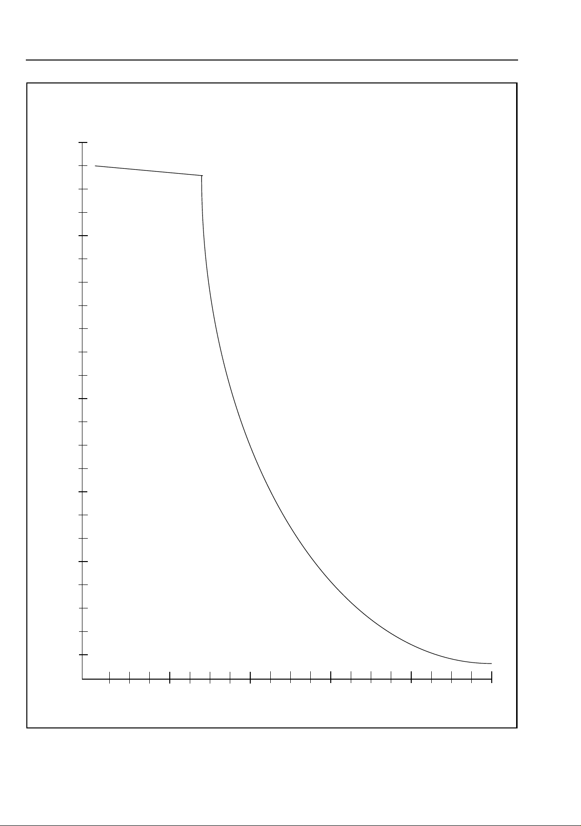
VBAT set at -48V. A typical Operating Current versus
Loop Resistance with VBAT at -48V is shown in
Figure 7.
UD & Line Drivers Overcurrent
Protection
The Line Drivers control the external Battery Feed
circuit which provide power to the line and allows bidirectional audio transmission.
Balanced Ringing & Automatic Ring
Tripping
Balanced Ringing is applied to the line by setting the
RC to +5V (pin 25) and connecting ringing signal
(20Hz) to RV (pin 35) as shown in Figure 4. A
1.2Vrms input will give approximately about 60Vrms
output across Tip and Ring, sufficient for short loop
SLIC application. The SLIC is capable of detecting
an Off Hook condition during ringing by filtering out
the large A.C. component. A 0.47uF cap should be
connected to pin CP6 (pin 29) to form such filter.
This filter allows a true Off Hook condition to be
monitored at pin SHK (pin 33). When an Off Hook
condition is detected by the SLIC, it will remove the
20Hz AC ringing voltage and revert to constant
current mode. The local controller will, however, still
need to deselect RC (set it to 0V).
The MT91610 supports short burst of ringing
cadence. A deglitching input (CP7) is provided to
ensure that the SHK pin is glitch free during the
assertion and de-assertion of RC. A 33nF cap
should be connected at this pin to GND.
The loop supervision circuitry provides bias to the
line drivers to feed a constant current. Overcurrent
protection is done by the following steps:
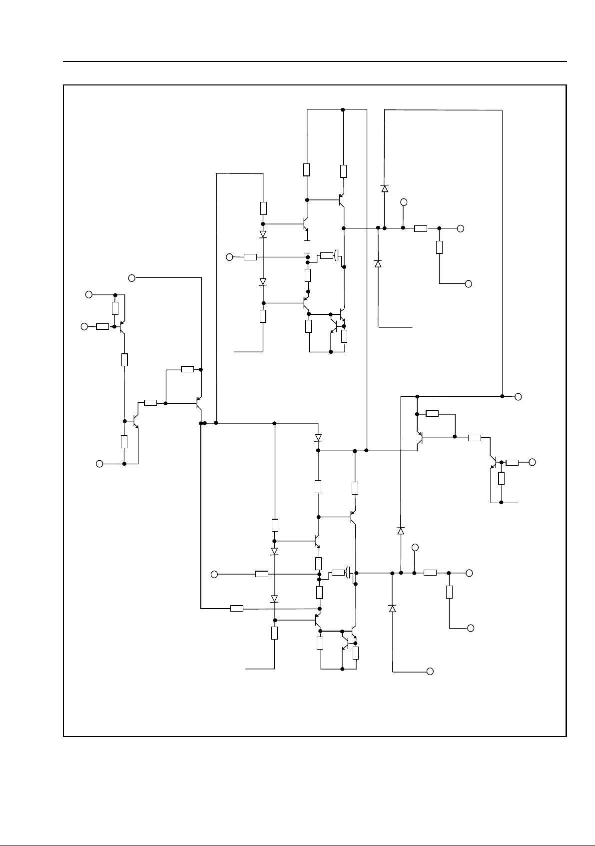
(A) External bipolar transistors to limit the current of
the NPN drivers to 50mA (Figure 5).
(B) The local controller should monitor the
Unbalance Detection output (UD) for any extended
period of assertion (>5 seconds). In such case the
controller should power down the de vice by asserting
the PD pin, and polls the device every 5 seconds.
The UD output can be used to support GND START
LOOP in a PaBX operation.
Please note that this UD output should be
disregarded and masked out if RC pin is active (ie
set to +5V).
Powering Up / Down Sequence
AGND is always connected
Powering Up: +5V, -5V, VBAT
PD to +5V for 100ms; PD to 0V
Powering Down: VBAT, -5V, +5V
A positive voltage source is required to be
connected to the pin DCRI (Figure 5) for normal
Ringing generation. The SLIC can perform ringing
even with the DCRI input connected to 0V. However,
it does require the VBAT to be lower than -48V (ie at
-53V or lower) and the 20Hz AC input should be a
square wave at 2Vrms.
Line Reversal
The MT91610 can deliver Line Reversal, which is
required in operation such as ANI, by simply setting
LR (pin 7) to +5V. The device transmission
parameters will cease during the reversal. The LR
(pin 7) should be set to 0V for all normal loop
operations.
Power Down And Wake Up
The MT91610 should normally be powered down to
conserve energy by setting the PD pin to +5V. The
SHK pin will be asserted if the equipment side (2
wire) goes off hook. The local controller should then
restore power to the SLIC for normal operations by
setting the PD pin to 0V.
Please note that there will be a short break (about
80ms) in the assertion time of SHK due to the time
required for the loop to power up and loop current to
flow. The local controller should be able to mask out
this time fairly easily.
5
Page 6

MT91610 Preliminary Information
Meter Pulse Injection
The MT91610 provides a gain path input (ESI) for
meter pulse injection and an independent control
logic input (ESE) for turning the meter pulse signal
on and off.
Additional circuit can be used to ensure good
cancellation of meter pulse signal (Figure 4) should it
becomes audible at the 4 wire side. Usually, the
optional circuit is not required.
Gain (meter pulse) = 20 Log [0.891 * (R10 / R11)]
Components Selection
Feed Resistors
The selection of feed resistors, Ra and Rb, can
significantly affect the performance of the MT91610.
The value of 100 Ω is used for both Ra and Rb.
The resistors should have a tolerance of 1% (0.1%
matched) and a power rating of 0.5 Watt.
Calculating Components Value
Step 2: Impedance Matching (R4, R5)
Zo / ( Ra+Rb) = kZo / R4 where kZo = R5
R5 / R4 = 3
∴ choose R4 = 100kΩ => R5 = 300kΩ
Step 3: Network Balance Impedance (R6)
Optimized Case Zo = Z
R6 = R7 * (R9 / R10) * 2.2446689 * ( ZNB / ZNB + Zo)
R6 = 300kΩ * (1) * 1.1223344
= 336.7kΩ
Step 4: The Loop Current (R2)
In order to remain in constant current mode during
normal operation, it is necessary that the following
equation holds:
{| I * Zt |} V < { | VBAT | - 6*VREF - 2} V
where,
I = Desirable Loop Current
Zt = Ra + Rb + maximum loop impedance
VBAT = Battery voltage
VREF= DC voltage at VREF pin
NB
There are five parameters a designer should know
before starting the component calculations. These
five parameters are:
1) characteristic impedance of the line Z
2) network balance impedance Z
3) value of the feed resistors (Ra and Rb)
4) 2W to 4W transmit gain
5) 4W to 2W receive gain
The following example will outline a step by step
procedure for calculating component values. Given:
Zo = 600Ω, ZNB= 600Ω, Ra=Rb= 100Ω
Gain 2 - 4 = -6dB, Gain 4 - 2 = -1 dB
Step 1: Gain Setting (R7, R8, R9, R10)
Gain 2 - 4 = 20 Log [ R8 / R7]
-6 dB = 20 Log [R8 / R7]
∴ choose R7 = 300kΩ, R8 = 150kΩ.
Gain 4 - 2 = 20 Log [0.891 * [R10 / R9)]
-1 dB = 20 Log [0.891 * [R10/ R9)]
∴ choose R9 = 200kΩ, R10 = 200kΩ.
NB
o
Given the parameters as follows:
Ra = Rb = 100 Ω
Expected maximum loop impedance = 1.6kΩ
(including Ra and Rb)
Desirable Loop Current = 20mA
6*Vref=8V
Then | VBAT | (min) = 1600 * 0.020 +10 = 42V
Assume that the VBAT of 42V is available, then read
the value of R2 from Figure 6, which is 50kΩ.
Step 5: Calculation Of Non-Clipping Sinusoidal
Ringing Voltage At Tip Ring (VTR)
Assume the Ringing Current is less than 40mA, the
ringing voltage (20Hz) at Tip and Ring is given as:
VTR (rms) = 0.707 * {| VBAT | + VDCRI - (15.6 *
VREF)}
VDCRI= Positive DC voltage at DCRI pin
VBAT = Negative Battery voltage
VREF= Positive DC voltage at VREF pin
AC voltage at the RV input pin is therefore
RV (rms)~= VTR (rms) / 50
6
Page 7
Preliminary Information MT91610
TIP
PR1
RING
TR_DRIVER_610B
PD
1
-5V
2
3
4
RC
5
VBAT
6
+5V
7
8
15
TF_BR
SHK
13
12
11
10
9
8
14
RF_BR
D1**
C7
NO CONNECT
NO CONNECT
R13
+5V
C14
R2
+5V
C12
C9
C5 C4
2
TD
3
TF1
4
NC
5
TIP
8
RING
9
RF1
10
NC
C2
6
VREF2
R1
12
CP1
C13
13
CP2
C1
14
CP3
15
CP4
136
Vdd
Vee
RV
Z1
CP5
Z2
Z3
GTX0
VX
ESI
GTX1
VR
UD
35
21
22
23
24
25
26
27
28
20
R8
31
32VBAT
C10
R11
-5V
R7
R10
VBAT
R6
R4
R9
R5
C6
RING VOLTAGE
R16
C8
VX_OUT
ESI
UNBALANCE DETECTION
VBAT_IN
VR_IN
DCRI_IN
PD
RC
SHK
C3
ESE
SWITCH HOOK
ESE
POWER DOWN
LINE REVERSE
RING CONTROL
C15
C11
18
DCRI
34
CP7
11
RD
AGND
SHK
CP6
ESE
PD
LR
RC
33
29
16
17
7
30
= Ground (Earth)
19
* See Functional Description Meter Pulse Injection
** Optional
Figure 4 - Typical Application with a Resistive 600 ohm Line Impedance
7
Page 8

MT91610 Preliminary Information
Component List
R11 = 100kΩ
R2 = See Figure 6
R1,9,10 = 200kΩ
R4 = 100kΩ
R5,7,16 = 300kΩ
R6 = 336k7Ω
R8 = 150kΩ
R13 = 51kΩ
C1,10 = 330nF, 5%
C2,4,5,7,8 = 100nF, 5%
C3 = 470nF, 5%
C6 = 4.7uF, 5%
C9 = 10nF, 5%
C11 = 33nF, 5%
C12 = 100nF, 5%
C13 = 220nF, 5%
C14,15 = 150nF, 5%
D1 = 1N5819 Schottky Diode (Optional)
All resistors are 1/4W, 1% unless otherwise indicated.
PR1 = This device must always be fitted to ensure damages does not occur from inductive loads.
For simple applications PR1 can be replaced by a single TVS, such as 1.5KE220C, across tip
and ring.
For applications requiring lightning and mains cross protection further circuitry will be required
and the following protection devices are suggested:
P2353AA, P2353AB (Teccor), THBT20011, THBT20012, THBT200S (SGS-Thomson),
TISP2290, TSSP8290L (T.I.)
TF_BR,RF_BR= Circuit Breaker
8
Page 9
Preliminary Information MT91610
VDD
PIN 1
PD
PIN 7
PIN 2
VEE
R21
R22
R23
R24
Vee
PIN 3
0V
Q3
R25
Q4
R3
R1
Q7
D3
RCI
PIN 13
0v
R26
Q13
R7
D4
R2
Vee
R4
R5
Q8
R6
Q14
Vbat
R31
D13
R13
C1
Q6
Q5
R8
R9
R18
D10
Vbat
D9
PIN 14
RF_BR
Q1
BR
R27
Ra
RF
PIN 10
PIN 11
R28
RING
Q3
PIN 4
R29
R30
0v
DCRI
RC
PIN 5
TCI
PIN 12
R11
Q9
D3
R17
D4
R31
R12
Vee
R14
R15
Q12
R16
Vbat
C2
R32
Q15
Figure 5 - Line Driver Stage
Q10
Q11
R19
D12
Vbat
D11
PIN 15
TF_BR
BR
PIN 6
PIN 8
TF
Rb
TIP
PIN 9
VBAT_IN
9
Page 10

MT91610 Preliminary Information
Component List
R1,3,6,11,13,16 = 2.5kΩ
R2,12 = 3.6kΩ
R4,5,14,15 = 470 Ω
R7,17,31,32 =360 Ω
R8,9,18,19 = 12 Ω
Ra, Rb = 100 Ω 1%, 0.15% matched 1W
R21,26,27,30 = 30kΩ
R22,25,28,29 = 3kΩ
R23,24 = 20kΩ
R21,26,27,30 = 3 kΩ
R31 = 5.1 kΩ
C1,2 = 10nF, 5%
D1-8,13 = 1N4148 or equivalent
D9,10,11,12 = 1N4005 or equivalent
Q1,3 = 2N2907
Q2,4,14,15= 2N2222
Q3 = BCP56
Q5,7,9,11 = MPSA42
Q6,8,10,12,13 = MPSA92
BR =Circuit Breaker
All resistors are 1/4W, 1% unless otherwise indicated.
10
Page 11
Preliminary Information MT91610
R2 (Kohm) vs Loop Current (mA)
145
140
135
130
125
120
115
110
105
100
95
90
85
80
75
70
65
R2 (Kohm)
60
55
50
15
16 17 18 19 20 21
22 23
Loop Current (mA)
24 25 26 27 28 29 30 31
Figure 6 - Approximated R2 (Kohm) Versus Programmed Loop Current (mA)
11
Page 12
MT91610 Preliminary Information
Loop Current (mA) versus Loop Resistance (Ohm)
31
30
29
28
26
25
24
23
22
21
20
19
18
17
16
15
14
13
12
11
10
12
9
8
0 200 400 600 800 1000 1200 1400 1600271800 2000 2200 2400 2600 2800 3000 3200 3400 3600 3800 4000
Loop Resistance (Ohm)
Figure 7 - Loop Current (mA) Versus Loop Resistance (ohm)
Page 13
Preliminary Information MT91610
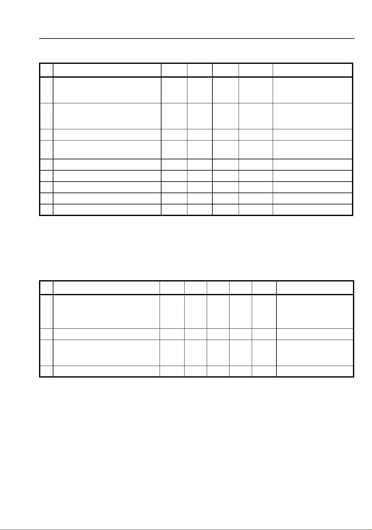
Absolute Maximum Ratings*
Parameter Sym Min Max Units Comments
.
1 DC Supply Voltages V
2 Ringing Voltages V
DD
V
EE
V
BAT
RING
-0.3
+0.3
+0.3
+6.5
-6.5
-72
70 V
V
V
V
RMS
Differentially across Tip &
Ring for a 1.5Vrms input
at RV (Figure 4)
3 Voltage setting for Loop Current V
4 Overvoltage Tip/GND Ring/GND,
REF
E
E
0 5 V Note 1
200 V MAX 1ms (with power on)
Tip/Ring
5 Ringing Current I
RING
35 mA
6 Tip / Ring Ground over-current 50 mA Note 2
7 Storage Temp T
8 Package Power Dissipation P
STG
DISS
-65 +150 ˚C
0.10 W +85˚C max, V
BAT
= -48V
9 ESD maximum rating 500 V
*Exceeding these values may cause permanent damage. Functional operation under these conditions is not implied.
Note 1: Refer to Figure 3 & 6 for appropriate biasing values
Note 2: Tip and Ring drivers to be limited to about 50mA externally (Figure 5). If the UD pin is asserted for longer than 5 seconds, then
PD should be asserted to power down the device. The device should then be checked (by de-asserting PD) every 5 seconds.
Recommended Operating Conditions
Parameter Sym Min Typ
1 Operating
Supply Voltages
2 Ringing Voltage V
3 Voltage setting for Loop Current V
4 Operating Temperature T
‡ Typical Figures are at 25˚C with nominal supply voltages and are for design aid only
Note 3: For a 1.2Vrms 20Hz input at RV terminal (Figure 4) and with RC pin set to +5V.
Note 4: Refer to Figure 3 & 6 for biasing values
V
DD
V
EE
V
BAT
DCRI
RING
REF
O
4.75
-5.25
-72
5
060 V
-40 +25 +85 ˚C
‡
Max Units Test Conditions
5.00
-5.00
-48
5.25
-4.75
-22
72
1.67 V I
V
V
V
V
RMS
50mA current capability
Note 3
= 25mA,
LOOP
VBAT = -48V
Note 4
13
Page 14

MT91610 Preliminary Information
DC Electrical Characteristics
Characteristics Sym Min Typ‡Max Units Test Conditions
1 Supply Current I
2 Supply Current I
3 Constant Current Line
Feed
4 Operating Loop Constant
Current Mode
(including the DC
resistance of the
Telephone Set)
5 Off Hook Detection
Threshold
6 RC, LR
Input Low Voltage
Input High Voltage
7 PD, ESE
Input Low Voltage
Input High Voltage
8 SHK
Output Low Voltage
Output High Voltage
9 UnBalance Detection
Threshold
†
I
I
BAT
I
I
BAT
I
LOOP
R
LOOP
S
V
V
V
V
V
V
I
DD
EE
DD
EE
HK
OL
OH
UD
Ω
Ω
PD= 0V
V
= -48V
BAT
l
~ l
BAT
PD = 5V
V
= -48V
BAT
=1.67V
REF
I
= 20mA
LOOP
V
= -48V
BAT
I
= 20mA
LOOP
V
= -22V
BAT
LOOP
+ 3 mA
8
6
28
300
300
1.8
mA
mA
mA
uA
uA
mA
25 mA V
1600
700
14 mA
IL
IH
IL
IH
4.5
4.5
0.5 V
0.5 V
0.4 V
2.7
V
V
V
LIL = -1µA
LIH = 1µA
LIL= -1µA
LIH = 1µA
LOL = 8mA
LOH = -1mA
12 mA
10 UD
Output Low Voltage
Output High Voltage
V
OL
V
OH
2.7
0.4 LOL = 0.3mA
11 Dial Pulse Distortion 1 ms
†
Electrical Characteristics are over Recommended Operating Conditions unless otherwise stated.
‡
Typical Figures are at 25°C with nominal ±5V and are for design aid only.
LOH = -0.3mA
14
Page 15

Preliminary Information MT91610
AC Electrical Characteristics
Characteristics Sym Min Typ
†
‡
Max Units Test Conditions
1 Ring Trip Detect Time Tt 90 200 mS
2 Impedance (2W) Z
O
3 Return Loss (2W) RL 20 30
4 Transhybrid Loss THL 20 25 dB
600 Ω
dB
300Hz to 3k4Hz
Note 5
5 Output Impedance at VX 10 Ω AC small signal
6 Gain 4 to 2 Wire @ 1kHz -1.5 -1 -0.5 dB Note 5
7 Gain Relative to 1kHz ±0.15 dB 300 - 3400Hz
8 Gain 2W to VX @ 1kHz -0.5 0 0.5 dB Note 5
9 Gain Relative to 1kHz ±0.15 dB 300Hz to 3.4KHz
10 Longitudinal to Metallic Balance
LCL 55 dB 300Hz to 3.4KHz
at 2W
11 Total Harmonic Distortion
@2W
@VX
12 Common Mode Rejection
THD
0.3
0.3
1.0
1.0
%
%
1Vrms, 1kHz @ 2W
1Vrms, 1KHz @ VR
CMR 45 50 dB Input 0.5Vrms, 1KHz
2 Wire to Vx
13 Idle Channel Noise
@2W
@VX
14 Power Supply Rejection
NC
PSR
12
12
dBrnC
dBrnC
Cmessage Filter Fig. 4
Cmessage Filter Fig. 4
Ratio at 2W and VX
Vdd
V ee
23
23
dB
dB
0.1Vp-p @ 1kHz
15 Line Reversal Recovery Timing TLRR 30 50 ms Note 6
†
Electrical Characteristics are over Recommended Operating Conditions unless otherwise stated.
‡
Typical Figures are at 25°C with nominal ±5V and are for design aid only.
Note 5: Refer to Figure 4 & 5 for set up and components value.
Note 6: TLRR is measured from the time when the LR pin is set to 0V (de-selected), to the time when the loop current is within 10% of
its programmed steady state value.
15
Page 16
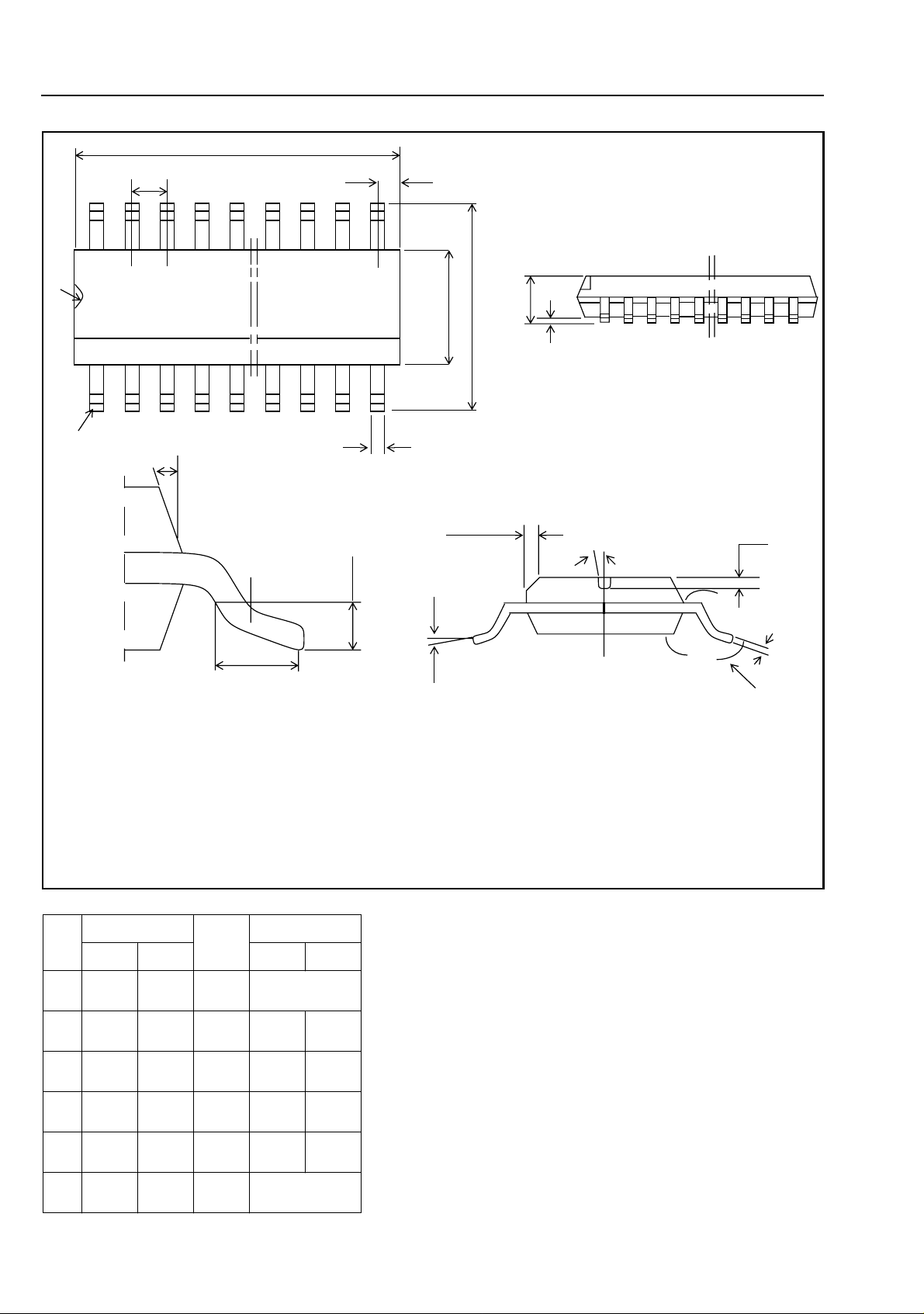
MT91610 Preliminary Information
D
R
Pin #1
e
7
GAGE
PLANE
0.335
ZD
(.014)
B
HE
±0.20
0.51 x 45°
±.008
(.020)
A
A1
±0.10
7
0.63
±.004
(.025)
C
L
Notes:
1. Lead Coplanitary should be 0 to 0.10mm (.004") max
2. Package surface finishing
(2.1) Top Matte: (Charmilles #18-30)
(2.2) All Sides: (Charmilles #18-30)
(2.3) Bottom Matte: (Charmilles #18-30)
3. All dimensions excluding mold flashes
4. Max. deviation of center of package and center of leadrame to be 0.10mm (.004")
5. Max. misalignment between top and bottom center of package to 0.10mm (.004")
6. End flash from the package body shall not exceed 0.152 (.006") per side (D)
7. Dimension B shall not include dambar protrusion/intrusion and solder coverage.
8. Not to scale
9. Dimension in inches
10.Dimensions in (millimeters)
a
QSOP - Quad Shrink Outline Package
Dim
36-Pin
Dim
36-Pin
Min Max Min Max
A .096
(2.44)
A
.004
1
(0.10)
B .011
(0.26)
C .0091
(0.23)
D .598
(15.20)
E .291
(7.40)
.104
(2.64)
.012
(0.30)
.020
(0.51)
.0125
(0.32)
.606
(15.40)
.299
(7.60)
e .0315 inches (ref)
0.80mm
H .398
(10.11)
L 0.16
(0.40)
Q 08
R .025
(0.63)
ZD .0335 inches (ref)
.414
(10.51)
.050
(1.27)
.035
(0.89)
0.85
Q
16
Page 17

Preliminary Information MT91610
Notes:
17
Page 18

http://www.mitelsemi.com
World Headquarters - Canada
Tel: +1 (613) 592 2122
Fax: +1 (613) 592 6909
North America Asia/Pacific Europe, Middle East,
Tel: +1 (770) 486 0194 Tel: +65 333 6193 and Africa (EMEA)
Fax: +1 (770) 631 8213 Fax: +65 333 6192 Tel: +44 (0) 1793 518528
Fax: +44 (0) 1793 518581
Information relating to products and services furnished herein by Mitel Corporation or its subsidiaries (collectively “Mitel”) is believed to be reliable. However, Mitel assumes no
liability for errors that may appear in this publication, or for liability otherwise arising from the application or use of any such information, product or service or for any infringement of
patents or other intellectual property rights owned by third parties which may result from such application or use. Neither the supply of such information or purchase of product or
service conveys any license, either express or implied, under patents or other intellectual property rights owned by Mitel or licensed from third parties by Mitel, whatsoever.
Purchasers of products are also hereby notified that the use of product in certain ways or in combination with Mitel, or non-Mitel furnished goods or services may infringe patents or
other intellectual property rights owned by Mitel.
This publication is issued to provide information only and (unless agreed by Mitel in writing) may not be used, applied or reproduced for any purpose nor form par t of any order or
contract nor to be regarded as a representation relating to the products or services concerned. The products, their specifications, services and other information appearing in this
publication are subject to change by Mitel without notice. No warranty or guarantee express or implied is made regarding the capability, performance or suitability of any product or
service. Information concerning possible methods of use is provided as a guide only and does not constitute any guarantee that such methods of use will be satisfactory in a specific
piece of equipment. It is the user’s responsibility to fully determine the performance and suitability of any equipment using such information and to ensure that any publication or
data used is up to date and has not been superseded. Manufacturing does not necessarily include testing of all functions or parameters. These products are not suitable for use in
any medical products whose failure to perform may result in significant injury or death to the user. All products and materials are sold and services provided subject to Mitel’s
conditions of sale which are available on request.
M Mitel (design) and ST-BUS are registered trademarks of MITEL Corporation
Mitel Semiconductor is an ISO 9001 Registered Company
Copyright 1999 MITEL Corporation
All Rights Reserved
Printed in CANADA
TECHNICAL DOCUMENTATION - NOT FOR RESALE
 Loading...