

Page 1
MT90826
Quad Digital Switch
Advanced Information
Features
• 4,096 × 4,096 channel non-blocking switching
at 8.192 or 16.384 Mb/s
• Per-channel variable or constant throughput
delay
• Accept ST-BUS streams of 2.048Mb/s,
4.096Mb/s, 8.192Mb/s, or 16.384 Mb/s
• Split Rate mode allows mix of two bit rates and
rate conversions
• Automatic frame offset delay measurement for
ST-BUS input and output streams
• Per-stream frame delay offset programming
• Per-channel high impedance output control
• Bit Error Monitoring on selected ST-BUS input
and output channels.
• Per-channel message mode
• Connection memory block programming
• IEEE-1149.1 (JTAG) Test Port
• 3.3V local I/O with 5V tolerant inputs and TTL
compatible outputs
Applications
• Medium and large switching platforms
• CTI application
• Voice/data multiplexer
• Digital cross connects
• WAN access system
• Wireless base stations
DS5197 ISSUE 2 June 1999
Ordering Information
MT90826AL 160 Pin MQFP
MT90826AG 160 Pin PBGA
-40 to +85 C
Description
The MT90826 Quad Digital Switch has a nonblocking s witch capacity of 4,096 x 4,096 channels at
a serial bit rate of 8.192Mb/s or 16.384 Mb/s, 2,048 x
2,048 channels at 4.096Mb/s and 1024 x 1024
channels at 2.048Mb/s. The device has many
features that are programmable on a per stream or
per channel basis, including message mode, input
offset delay and high impedance output control.
The per stream input and output delay control is
particularly useful for managing large multi-chip
switches with a distributed backplane.
Operating in Split Rate mode allows for switching
between two groups of bit rate streams.
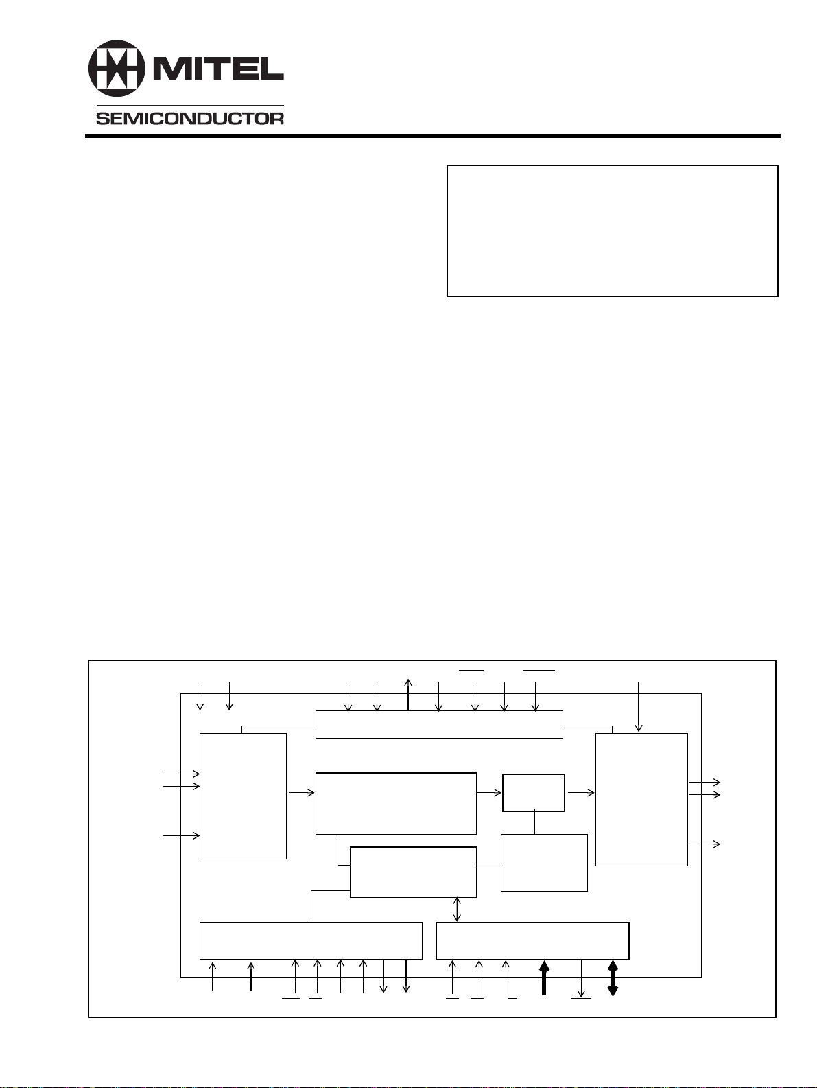
STi0/FEi0
STi1/FEi1
•
•
•
STi31/FEi31
V
DD
PLLV
V
SS
Serial
to
Parallel
Converter
DD
SS
TDI TDO IC1 RESETTCK TRST
TMS
Test Port
Multiple Buffer
Data Memory
Internal
Registers
Timing
Unit
F0i DS CS R/W A13-A0 DTA D15-D0
CLK
IC3PLLV
DT1 AT1IC2
Microprocessor Interface
Output
MUX
Connection
Memory
Figure 1 - Functional Block Diagram
ODE
Parallel
to
Serial
Converter
STo0
STo1
•
•
•
STo31
1
Page 2
MT90826 CMOS Advanced Information
STo16
STo17
STo18
NC
STo20
STo21
STi22/FEi22
STi23/FEi23
VSS
STi21/FEi21
STo19
STi20/FEi20
VDD
VSS
STi18/FEi18
STi19/FEi19
VSS
STi16/FEi16
STi17/FEi17
VSS
VDD
STo15
STo14
STo13
STo12
STi15/FEi15
STi14/FEi14
VSS
STi12/FEi12
STi13/FEi13
VSS
VDD
STo10
STo11
STo9
STo8
VSS
STi10/FEi10
STi11/FEi11
NC
NC
STo22
STo23
VSS
VDD
STi24/FEi24
STi25/FEi25
STI26/FEi26
STi27/FEi27
VSS
STo24
STo25
STo26
STo27
VSS
VDD
STi28/FEi28
STi29/FEi29
STi30/FEi30
STi31/FEi31
VSS
STo28
STo29
STo30
STo31
VSS
VDD
D0
D1
D2
D3
D4
D5
D6
D7
VSS
VDD
D8
NC
NC
121
123
125
127
129
131
133
135
137
139
141
143
145
147
149
151
153
155
157
159
119
117
115
113
109111
107
105
103
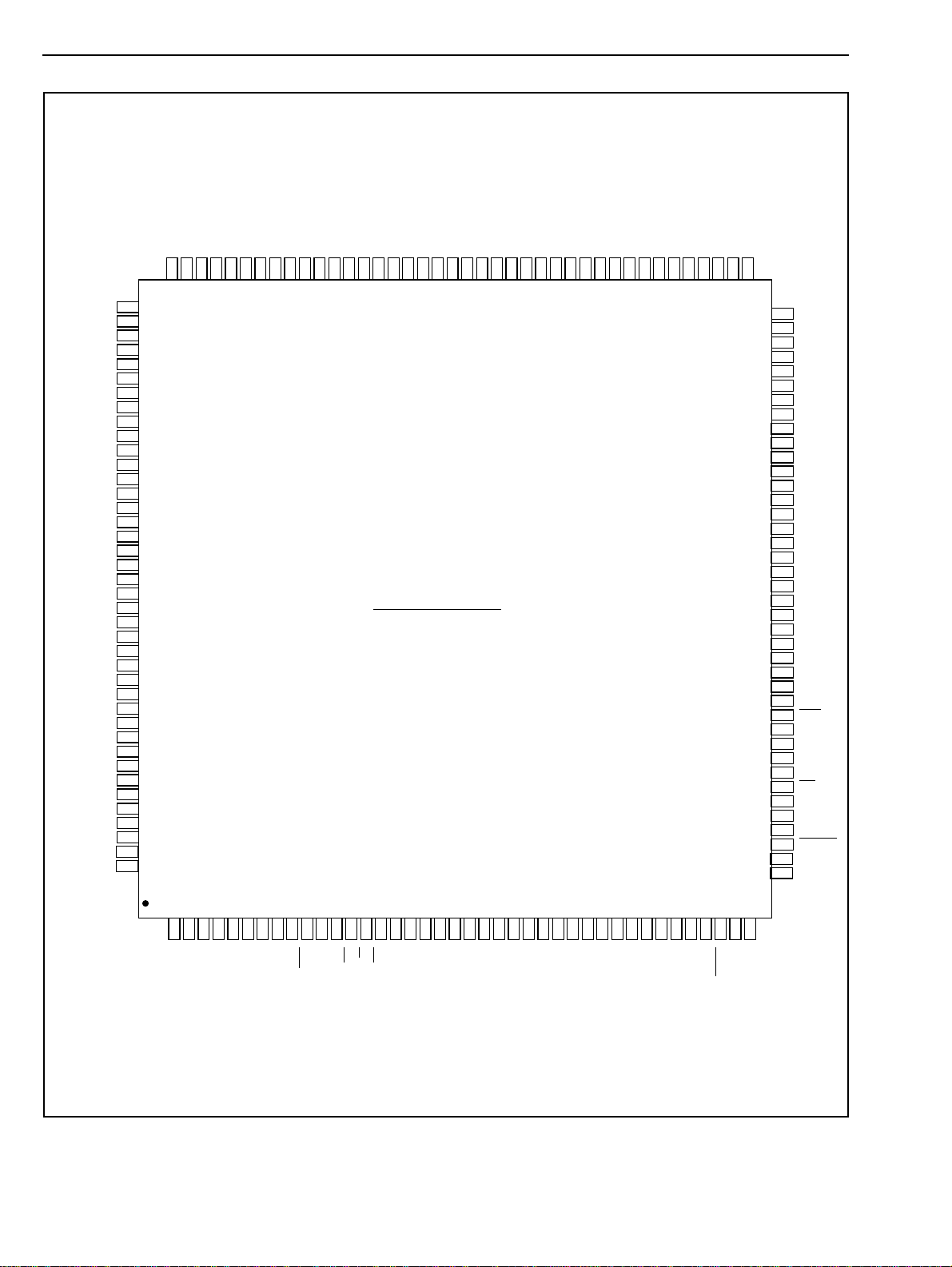
160 Pin MQFP
28mm x 28mm
Pin Pitch 0.65mm
101
959799
91
93 89
87 8385 81
NC
79
77
75
73
71
69
67
65
63
61
59
57
55
53
51
49
47
45
43
41
STi9/FEi9
STi8/FEi8
VDD
VSS
STo7
STo6
STo5
STo4
VSS
STi7/FEi7
STi6/FEi6
STi5/FEi5
STi4/FEi4
VDD
VSS
STo3
STo2
STo1
STo0
VSS
STi3/FEi3
STi2/FEi2
STi1/FEi1
STi0/FEi0
ODE
VDD
VSS
CLK
PLLVDD
PLLGND
DT1
AT1
F0i
IC3
VSS
IC2
RESET
IC1
XTM2
1
NC
NC
D9
D10
D11
D12
D13
D14
D15
CS
DTA
VSS
VDD
171513119 25 27232119753 29 31
W
DS
R/
A0
A1
A2
A3
A4
VSS
VDD
A5
A6
A7
A8
A9
A10
A11
33 35 37 39
A12
A13
VSS
VDD
TMS
TDI
TDO
TCK
NC
TRST
XTM1
Figure 2 - 160-Pin MQFP Pin Connections
2
Page 3
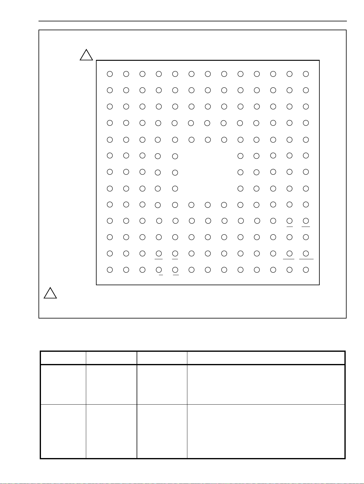
Advanced Information CMOS MT90826
1
A
B
C
D
E
F
G
H
J
K
L
M
N
12345678910111213
STi26 STi24 STo20 STi22 STi20 STi18 STi16 STo15 ST013 STo10 STo8 STi10 STi9
STi27 STi25 STo21 STi23 STi21 STi19 STi17 STo14 STo12 STo11 STo9 STi11 STi8
STo26 STo25 STo23 STo19 STo18 STo17
STo22STo24STo27
VDD
STi28 NCSTi30
STi29 NCSTi31
STo28 STo29
STo30 STo31 D2
D1 D3
D5 D6
D10
D13
D9D8
D11
D14
D0
D4
D7
NC
D12
D15NCR/W
GND
VDD
GND
VDD
GND
VDD
VDD
GND
GND GNDGNDGNDGND
NC
DTA CS A0 A3 A8A7 A11 TDI TRST
NC
A1DS A2 A4 A5 A6 TMS
TOP VIEW
VDDVDDVDDGND
A9
NC
A10
STi13
STi14
VDDVDDVDDVDDVDDGND GND
VDD
GNDGNDGNDGND
VDD
GND
VDD
GND
GND
GND
VDD
PLLVDD
PLLGND
A12 A13
STo2
STo1 STi4STi5
STo0
XTM2
DT1
XTM1
IC1
STo5
STo7STi12STi15STo16
STo4
STo6STo3
STi6STi7
STi3
STi2
STi0STi1
ODEAT1
CLKF0i
IC2 IC3
RESET
TDO TCK
1 - A1 corner is identified by metallized markings.
23mm x 23mm
Ball Pitch 1.5mm
Figure 3 - 160-Pin PBGA Pin Connections
Pin Description
Pin # MQFP Pin # PBGA Name Description
12,22,33,54,
66,77,90,101,
112,125,136,
147,157
11,21,32,45,
53,60,65,71,
76,84,89,95,
100,106,111,
117,124,130,
135,141,146,
156
D5,D6,D7,D8,D9,
E4,E10,F4,
F10,G4,G10,
H4,J4,J10,K5,
K6,K7
D4,D10,E5,E6,E7
,
E8,E9,F5,F9,G5,
G9,H5,H9,H10,J5
,
J6,J7,J8,J9,K4
V
DD
V
ss
+3.3 Volt Power Supply
Ground
3
Page 4

MT90826 CMOS Advanced Information
Pin Description (continued)
Pin # MQFP Pin # PBGA Name Description
34 N11 TMS Test Mode Select (3.3V Input with Internal pull-up):
JTAG signal that controls the state transitions of the TAP
controller. This pin is pulled high by an internal pull-up
when not driven.
35 M11 TDI Test Serial Data In (3.3V Input with Internal pull-up):
JTAG serial test instructions and data are shifted in on
this pin. This pin is pulled high by an internal pull-up when
not driven.
36 N12 TDO Test Serial Data Out (3.3V Output): JTAG serial data is
output on this pin on the falling edge of TCK. This pin is
held in high impedance state when JTAG scan is not
enabled.
37 N13 TCK Test Cloc k (5V Tolerant Input): Provides the clock to the
JTAG test logic.
38 M12 TRST Test Reset (3.3V Input with internal pull-up):
Asynchronously initializes the JTAG TAP controller by
putting it in the Test-Logic-Reset state. This pin is pulled
by an internal pull-up when not driven. This pin should be
pulsed low on power-up, or held low, to ensure that the
device is in the normal functional mode.
40 K11 XTM1 PLL Test Access 1 (3.3V Input): Use for PLL testing
only. No connect for normal operation.
41 J11 XTM2 PLL Test Access 1 (3.3V Input): Use for PLL testing
only. No connect for normal operation.
42 L11 IC1 Internal Connection 1 (3.3V Input with internal pull-
down): Connect to VSS for normal operation.
43 M13 RESET Device Reset (5V Tolerant Input): This input (active
LOW) puts the device in its reset state which clears the
device internal counters and registers.
44 L12 IC2 Internal Connection 2 (3.3V Input with internal pull-
down): Connect to VSS for normal operation.
When IC3 pin is tied to 3.3V, this pin is used as the PLL
bypass clock input for PLL testing only.
46 L13 IC3 Internal Connection 3 (3.3V Input with internal pull-
down): Connect to VSS for normal operation.
When this pin is tied to 3.3V, it enables the PLL bypass
mode for PLL testing only.
47 K12 F0i Master Frame Pulse (5V Tolerant Input): This input
accepts a 60ns wide negative frame pulse.
48 J12 AT1 Analog Test Access (Bidirectional):Use for PLL testing
only. No connect for normal operation.
49 H11 DT1 Digital Test Access Output (Output): Use for PLL
testing only. No connect for normal operation.
50 K10 PLLGND Phase Lock Loop Ground.
51 K9 PLLVDD Phase Lock Loop Power Supply: 3.3V
4
Page 5

Advanced Information CMOS MT90826
Pin Description (continued)
Pin # MQFP Pin # PBGA Name Description
52 K13 CLK Master Clock (5V Tolerant Input): Serial clock for
shifting data in/out on the serial streams. This pin accepts
a clock frequency of 8.192MHz or 16.384 MHz. The CPLL
bit in the control register determines the usage of the
clock frequency. See Table 6 for details.
55 J13 ODE Output Drive Enable (5V Tolerant Input): This is the
output-enable control pin for the STo0 to STo31 serial
outputs. See Table 2 for details.
56
57
58
59
67-70
78,79
82,83
91-94
102-105
113-116
126-129
137-140
61-64
72-75
85-88
96-99
107-110
118,119
122,123
131-134
142-145
148-153
154,155
158
3-7
8,9
H13
H12
G13
G12
F13,F12,E13,E12
B13,A13
A12,B12
C11,C10,C9,C8
A7,B7,A6,B6
A5,B5,A4,B4
A2,B2,A1,B1
E2,F2,E1,F1
G11,F11,E11,D11
D13,C13,D12,C12
A11,B11,A10,B10
B9,A9,B8,A8
C7,C6,C5,C4
A3,B3
D3,C3
D2,C2,C1,D1
G1,G2,H1,H2
G3,J1,H3,J2,J3,K1,
K2,K3
L1
L2,M1,M2,M3,N1,
N2,N3
STi0/FEi0,
STi1/FEi1
STi2/FEi2
STi3/FEi3
STi4-7/FEi4-7
STi8-9/FEi8-9
STi10-11/FEi10-11
STi12-15/FEi12-15
STi16-19/FEi16-19
STi20-23/FEi20-23
STi24-27/FEi24-27
STi28-31/FEi28-31
STo0 - 3
STo4 - 7
STo8 - 11
STo12 - 15
STo16 - 19
STo20, STo21
STo22, STo23
STo24 - 27
STo28 - 31
D0 - 5,
D6,D7
D8
D9 - 13
D14,D15
Serial Input Streams 0 to 31 and Frame Evaluation
Inputs 0 to 31 (5V Tolerant Inputs): Serial data input
streams. These streams may have data rates of 2.048,
4.096, 8.192 or 16.384 Mb/s, depending upon the value
programmed at bits DR0 - DR2 in the control register. In
the frame evaluation mode, they are used as the frame
evaluation inputs.
ST-BUS Output 0 to 31 (Three-state Outputs). Serial
data output streams. These streams may have data rates
of 2.048, 4.096, 8.192, or 16.384 Mb/s, depending upon
the value programmed at bits DR0 - DR2 in the control
register.
Data Bus 0 -15 (5V Tolerant I/O): These pins form the
16-bit data bus of the microprocessor port.
10 M4 DTA Data Transfer Acknowledgment (Three-state Output):
This output pulses low from tristate to indicate that a
databus transfer is complete . A pull-up resistor is required
to hold a HIGH level when the pin is tristated.
15 N5 DS Data Strobe (5V Tolerant Input): This active low input
works in conjunction with CS to enable the read and write
operations.
14 N4 R/W Read/Write (5V Tolerant Input): This input controls the
direction of the data bus lines (D0-D15) during a
microprocessor access.
13 M5 CS Chip Select (5V Tolerant Input): Active low input used
by a microprocessor to activate the microprocessor port.
16-20
23-31
1,2,39,80,81,120,
121,159,160
M6,N6,N7,M7,N8
N9,N10,M8,M9,L7
L8,M10,L9,A10
E3,F3,K8,
L3,L4,L5,L6
A0 - A4
A5-A13
Address 0 - 13 (5V Tolerant Input): These lines provide
the A0 - A13 address lines when accessing the internal
registers or memories.
NC No Connect
5
Page 6
MT90826 CMOS Advanced Information
Device Overview
The MT90826 Quad Digital Switch is capable of
switching up to 4,096 × 4,096 channels. The
MT90826 is designed to switch 64 kbit/s PCM or N x
64k bit/s data. The device maintains frame integrity
in data applications and minimum throughput delay
for voice applications on a per channel basis.
The serial input streams of the MT90826 can have a
bit rate of 2.048, 4.096, 8.192 or 16.384 Mbit/s and
are arranged in 125µs wide frames, which contain
32, 64,128 or 256 channels, respectively. The data
rates on input and output streams match. All inputs
and outputs may be programmed to 2.048, 4.096 or
8.192 Mb/s. STi0-15 and STo0-15 may be set to
16.384 Mb/s. Combinations of two bit rates,N and
2N
are provided. See Table 1.
By using Mitel’s message mode capability, the
microprocessor can access input and output
timeslots on a per channel basis. This feature is
useful for transferring control and status information
for external circuits or other ST-BUS devices.
The frame offset calibration function allows users to
measure the frame offset delay for streams STi0 to
STi31. The offset calibration is activated by a frame
evaluation bit in the frame evaluation register. The
evaluation result is stored in the frame evaluation
registers and can be used to program the input offset
delay for individual streams using internal frame
input offset registers.
The microport interface is compatible with Motorola
non-multiplexed buses. Connection memory
locations may be directly written to or read from; data
memory locations may be directly read from. A DTA
signal is provided to hold the bus until the
asynchronous microport operation is queued into the
device. For applications that require no wait states,
indirect reading and writing may be used.
Intermediary registers are directly programmed with
the write data and address, or read address. The
data in the intermediary registers is internally
transferred synchronous with the operation of the
internal state machines. Completion of the operation
is indicated by a status register flag.
Functional Description
A functional Block Diagram of the MT90826 is shown
in Figure 1.
Data and Connection Memory
For all data rates, the received serial data is
converted to parallel format by internal serial-toparallel converters and stored sequentially in the
data memory. Depending upon the selected
operation programmed in the control register, the
usable data memory may be as large as 4,096 bytes.
The sequential addressing of the data memory is
performed by an internal counter, which is reset by
the input 8 kHz frame pulse (F0i) to mark the frame
boundaries of the incoming serial data streams.
Data to be output on the serial streams may come
from either the data memory or connection memory.
Serial Interface Mode Input Stream Input Data Rate Output Stream Output Data Rate
8 Mb/s STi0-31 8 Mb/s STo0-31 8 Mb/s
16 Mb/s STi0-15 16 Mb/s STo0-15 16 Mb/s
4 Mb/s and 8 Mb/s STi0-15 4 Mbs/ STo0-15 4 Mb/s
STi15-31 8 Mb/s STo16-31 8 Mb/s
16 Mb/s and 8 Mb/s STi0-11 16 Mb/s STo0-11 16 Mb/s
STi12-19 8 Mb/s STo12-19 8 Mb/s
4 Mb/s STi0-31 4 Mb/s STo0-31 4 Mb/s
2 Mb/s and 4 Mb/s STi0-15 2 Mb/s STo0-15 2 Mb/s
STi16-31 4 Mb/s STo16-31 4 Mb/s
2 Mb/s STi0-31 2 Mb/s STo0-31 2 Mb/s
Table 1 - Stream Usage and External Clock Rates
6
Page 7

Advanced Information CMOS MT90826
Locations in the connection memory are associated
with particular ST-BUS output channels. When a
channel is due to be transmitted on an ST-BUS
output, the data for this channel can be switched
either from an ST-BUS input in connection mode, or
from the lower half of the connection memory in
message mode. Data destined for a particular
channel on a serial output stream is read from the
data memory or connection memory during the
previous channel timeslot. This allows enough time
for memory access and parallel-to-serial conversion.
Connection and Message Modes
In the connection mode, the addresses of the input
source data for all output channels are stored in the
connection memory. The connection memory is
mapped in such a way that each location
corresponds to an output channel on the output
streams. For details on the use of the source
address data (CAB and SAB bits), see Table 18.
Once the source address bits are programmed by
the microprocessor, the contents of the data memory
at the selected address are transferred to the
parallel-to-serial converters and then onto an STBUS output stream.
drivers and bit error test pattern enable. If an output
channel is set to a high-impedance state by setting
the OE bit to zero in the connection memory, the STBUS output will be in a high impedance state for the
duration of that channel. In addition to the perchannel control, all channels on the ST-BUS outputs
can be placed in a high impedance state by pulling
the ODE input pin low and programming the output
stand by (OSB) bit in the control register to low. This
action overrides the individual per-channel
programming by the connection memory bits. See
Table 2 for detail.
The connection memory data can be accessed via
the microprocessor interface through the D0 to D15
pins. The addressing of the device internal registers,
data and connection memories is performed through
the address input pins and the Memory Select (MS)
bit of the control register.
Clock Timing Requirements
The master clock (CLK) frequency must be either at
8.192 or 16.384MHz for serial data rate of 2.048,
4.096, 8.192 and 16.384Mb/s; see Table 6 for the
selections of the master clock frequency.
By having several output channels connected to the
same input source channel, data can be broadcasted
from one input channel to several output channels.
In message mode, the microprocessor writes data to
the connection memory locations corresponding to
the output stream and channel number. The lower
half (8 least significant bits) of the connection
memory content is transferred directly to the parallelto-serial converter. This data will be output on the
ST-BUS streams in every frame until the data is
changed by the microprocessor.
The three most significant bits of the connection
memory controls the following for an output channel:
message or connection mode, constant or variable
delay mode, enables/tristate the ST-BUS output
ODE pin OSB bit in Control register OE bit in Connection Memory ST-BUS Output Driver
0 0 X High-Z
X X 0 Per Channel High-Z
Switching Configurations
The MT90826 maximum non-blocking switching
configurations is determined by the data rates
selected for the serial inputs and outputs. The
switching configuration is selected by three DR bits
in the control register. See Table 5 and Table 6.
8Mb/s mode (DR2=0, DR1=0, DR0=0)
When the 8Mb/s mode is selected, the device is
configured with 32-input/32-output data streams
each having 128 64Kbit/s channels. This mode
allows a maximum non-blocking capacity of 4,096 x
4,096 channels. Table 1 summarizes the switching
configurations and the relationship between different
serial data rates and the master clock frequencies.
1 0 1 Enable
0 1 1 Enable
1 1 1 Enable
Table 2 - Output High Impedance Control
7
Page 8

MT90826 CMOS Advanced Information
16Mb/s mode (DR2=0, DR1=0, DR0 =1)
When the 16Mb/s mode is selected, the device is
configured with 16-input/16-output data streams
each having 256 64Kbit/s channels. This mode
allows a maximum non-blocking capacity of 4,096 x
4,096 channels.
4Mb/s and 8Mb/s mode (DR2=0, DR1=1, DR0=0)
When the 4Mb/s and 8Mb/s mode is selected, the
device is configured with 32-input/32-output data
streams. STi0-15/STo0-15 have a data rate of 4Mb/s
and STi16-31/STo16-31 have a data rate of 8Mb/s.
This mode allows a maximum non-blocking capacity
of 3,072 x 3,072 channels.
16Mb/s and 8Mb/s mode (DR2=0, DR1=1, DR0=1)
When the 16Mb/s and 8Mb/s mode is selected, the
device is configured with 20-input/20-output data
streams. STi0-11/STo0-11 have a data rate of 16Mb/
s and STi12-19/STo12-19 have a data rate of 8Mb/s.
This mode allows a maximum non-blocking capacity
of 4,096 x 4,096 channels.
4Mb/s mode (DR2=1, DR1=0, DR0=0)
When the 4Mb/s mode is selected, the device is
configured with 32-input/32-output data streams
each having 64 64Kbit/s channels. This mode allows
a maximum non-blocking capacity of 2,048 x 2,048
channels.
2Mb/s and 4Mb/s mode (DR2=1, DR1=0, DR0=1)
When the 2Mb/s and 4Mb/s mode is selected, the
device is configured with 32-input/32-output data
streams. STi0-15/STo0-15 have a data rate of 2Mb/s
and STi16-31/STo16-31 have a data rate of 4Mb/s.
This mode allows a maximum non-blocking capacity
of 1,536 x 1,536 channels.
2Mb/s mode (DR2=1, DR1=1, DR0 =0)
When the 2Mb/s mode is selected, the device is
configured with 32-input/32-output data streams
each having 32 64Kbit/s channels. This mode allows
a maximum non-blocking capacity of 1,024 x 1,024
channels.
Serial Input Frame Alignment Evaluation
The MT90826 provides the frame evaluation inputs,
FEi0 to FEi31, to determine different data input
delays with respect to the frame pulse
the frame evaluation input select bits (FE0 to FE4) of
the frame alignment register (FAR), users can select
one of the thirty-two frame evaluation inputs for the
frame alignment measurement.
F0i. By using
The internal master clock, which has a fixed
relationship with the CLK and F0i depending upon
the mode of operation, is used as the reference
timing signal to determine the input frame delays.
See Figure 4 for the signal alignments between the
internal and the external master clocks.
A measurement cycle is started by setting the start
frame evaluation (SFE) bit low for at least one frame.
Then the evaluation starts when the SFE bit in the
control register is changed from low to high. Two
frames later, the complete frame evaluation (CFE) bit
of the frame alignment register changes from low to
high to signal that a valid offset measurement is
ready to be read from bits 0 to 9 of the FAR register.
The SFE bit must be set to zero before a new
measurement cycle started.
The falling edge of the frame measurement signal
(FEi) is evaluated against the falling edge of the
frame pulse (F0i). See Table 7 for the description of
the frame alignment register.
Input Frame Offset Selection
Input frame offset selection allows the channel
alignment of individual input streams, which operate
at 4.096Mb/s, 8.192Mb/s or 16.384Mb/s, to be
shifted against the input frame pulse (F0i). The input
offset selection is not available for streams operated
at 2.048Mb/s. This feature is useful in compensating
for variable path delays caused by serial backplanes
of variable lengths, which may be implemented in
large centralized and distributed switching systems.
Each input stream has its own delay offset value
programmed by the input delay offset registers. Each
delay offset register can control 4 input streams.
There are eight delay offset registers (DOS0 to
DOS7) to control 32 input streams. Possible
adjustment can range up to +4.5 internal master
clock periods forward with resolution of 1/2 internal
master clock period. See Table 8 and Table 9 for
frame input delay offset programming.
Output Advance Offset Selection
The MT90826 allows users to advance individual
output streams up to 45ns with a resolution of 15ns
when the device is in 8Mb/s, 16Mb/s, 4 and 8 Mb/s or
16 and 8 Mb/s mode. The output delay adjustment is
useful in compensating for variable output delays
caused by various output loading conditions. The
frame output offset registers (FOR0 & FOR3) control
the output offset delays for each output streams via
the programming of the OFn bits.
8
Page 9

Advanced Information CMOS MT90826
See Table 10 and Table 11 for the frame output offset
programming.
Memory Block Programming
The MT90826 provides users with the capability of
initializing the entire connection memory block in two
frames. Bits 13 to 15 of every connection memory
location will be programmed with the pattern stored
in bits 13 to 15 of the control register.
The block programming mode is enabled by setting
the memory block program (MBP) bit of the control
register high. When the block programming enable
(BPE) bit of the control register is set to high, the
block programming data will be loaded into the bits
13 to 15 of every connection memory location. The
other connection memory bits (bit 0 to 12) are loaded
with zeros. When the memory block programming is
complete, the device resets the BPE bit to zero.
Bit Error Monitoring
Delay Through the MT90826
The switching of information from the input serial
streams to the output serial streams results in a
throughput delay. The device can be programmed to
perform timeslot interchange functions with different
throughput delay capabilities on the per-channel
basis. For voice application, select variable
throughput delay to ensure minimum delay between
input and output data. In wideband data applications,
select constant throughput delay to maintain the
frame integrity of the information through the switch.
The delay through the device varies according to the
type of throughput delay selected by the TM bits in
the connection memory.
Variable Delay Mode (TM1=0, TM0=0)
The delay in this mode is dependent only on the
combination of source and destination channels and
is independent of input and output streams.
The MT90826 allows users to perform bit error
monitoring by sending a pseudo random pattern to a
selected ST-BUS output channel and receiving the
pattern from a selected ST-BUS input channel. The
pseudo random pattern is internally generated by the
device with the polynomial of 215 -1.
Users can select the pseudo random pattern to be
presented on a ST-BUS channel by programming the
TM0 and TM1 bits in the connection memory. When
TM0 and TM1 bits are high, the pseudo random
pattern is output to the selected ST-BUS output
channel. The pseudo random pattern is then
received by a ST-BUS input channel which is
selected using the BSA and BCA bits in the bit error
rate input register (BISR). An internal bit error
counter keeps track of the error counts which is then
stored in the bit error count register (BECR).
The bit error test is enabled and disabled by the
SBER bit in the control register. Setting the bit from
zero to one initiates the bit error test and enables the
internal bit error counter. When the bit is
programmed from one to zero, the internal bit error
counter transfers the error counts to the bit error
count register.
In the control register, a zero to one transition of the
CBER bit resets the bit error count register and the
internal bit error counter.
Constant Delay Mode (TM1=1, TM0=0)
In this mode, frame integrity is maintained in all
switching configurations by making use of a multiple
data memory buffer.
Microprocessor Interface
The MT90826 provides a parallel microprocessor
interface for non-multiplexed bus structures. This
interface is compatible with Motorola non-multiplexed
buses. The required microprocessor signals are the
16-bit data bus (D0-D15), 14-bit address bus (A0A13) and 4 control lines (CS, DS, R/W and DTA).
See Figure 14 for Motorola non-multiplexed
microport timing.
The MT90826 microport provides access to the
internal registers, connection and data memories. All
locations provide read/write access except for the
data memory, DRR and BECR registers which are
read only.
For data memory read operations, two consecutive
microprocessor cycles are required. The read
address (A0-A13) should remain the same for the
two consecutive read cycles. The data memory
content from the first read cycle should be ignored.
The correct data memory content will be presented
to the data bus (D0-D15) on the second read cycle.
9
Page 10

MT90826 CMOS Advanced Information
A13 A12 A11 A10 A9 A8 A7 A6 A5 A4 A3 A2 A1 A0 Location
0 0 0 0 0 0 0 0 0 0 0 0 0 0 Control Register, CR
0 0 0 0 0 0 0 0 0 0 0 0 0 1 Frame Alignment Register, FAR
0 0 0 0 0 0 0 0 0 0 0 0 1 0 Input Offset Selection Register 0, DOS0
0 0 0 0 0 0 0 0 0 0 0 0 1 1 Input Offset Selection Register 1, DOS1
0 0 0 0 0 0 0 0 0 0 0 1 0 0 Input Offset Selection Register 2, DOS2
0 0 0 0 0 0 0 0 0 0 0 1 0 1 Input Offset Selection Register 3, DOS3
0 0 0 0 0 0 0 0 0 0 0 1 1 0 Input Offset Selection Register 4, DOS4
0 0 0 0 0 0 0 0 0 0 0 1 1 1 Input Offset Selection Register 5, DOS5
0 0 0 0 0 0 0 0 0 0 1 0 0 0 Input Offset Selection Register 6, DOS6
0 0 0 0 0 0 0 0 0 0 1 0 0 1 Input Offset Selection Register 7, DOS7
0 0 0 0 0 0 0 0 0 0 1 0 1 0 Frame Output Offset Register, FOR0
0 0 0 0 0 0 0 0 0 0 1 0 1 1 Frame Output Offset Register, FOR1
0 0 0 0 0 0 0 0 0 0 1 1 0 0 Frame Output Offset Register, FOR2
0 0 0 0 0 0 0 0 0 0 1 1 0 1 Frame Output Offset Register, FOR3
0 0 0 0 0 0 0 0 0 0 1 1 1 0 Unused
0 0 0 0 0 0 0 0 0 0 1 1 1 1 Unused
0 0 0 0 0 0 0 0 0 1 0 0 0 0 Unused
0 0 0 0 0 0 0 0 0 1 0 0 0 1 Bit Error Input Selection Register, BISR
0 0 0 0 0 0 0 0 0 1 0 0 1 0 Bit Error Count Register, BECR
Table 3 - Address Map for Registers (A13 = 0)
Stream Address (ST0-31) Channel Address (Ch0-255)
A13
A12 A11 A10 A9 A8
1
0
0
0
1
0
1
1
1
1
1
1
1
.
.
.
1
1
1
1
1
1
1
1
1
1
1. Bit A13 must be high for access to data and connection memory positions. Bit A13 must be low for access to registers.
2. Channels 0 to 31 are used when serial stream is at 2Mb/s.
3. Channels 0 to 63 are used when serial stream is at 4Mb/s
4. Channels 0 to 127 are used when serial stream is at 8Mb/s
5. Channels 0 to 255 are used when serial stream is at 16Mb/s
0
0
0
0
0
0
0
0
0
0
0
0
0
0
1
.
.
.
.
.
.
1
0
1
0
1
1
1
1
1
1
1
1
1
1
1
1
1
1
1
1
0
0
0
0
1
0
1
1
0
1
0
1
1
1
1
0
0
.
.
.
1
1
1
1
0
0
0
0
0
1
0
1
1
0
1
0
1
1
1
1
0
1
0
1
0
1
0
1
0
.
.
.
.
.
.
0
1
0
1
0
1
0
1
0
1
Stream
Location
Stream 0
Stream 1
Stream 2
Stream 3
Stream 4
Stream 5
Stream 6
Stream 7
Stream 8
.
.
.
Stream 22
Stream 23
Stream 24
Stream 25
Stream 26
Stream 27
Stream 28
Stream 29
Stream 30
Stream 31
A7 A6 A5 A4 A3 A2 A1 A0
0
0
0
0
0
0
0
0
0
0
.
.
.
0
0
0
0
.
.
0
0
0
0
.
0
0
1
1
.
1
1
.
.
.
0
0
0
0
0
1
0
1
.
.
.
.
0
1
0
1
1
0
1
0
.
.
1
1
1
1
0
0
0
0
.
.
1
1
1
1
0
.
.
.
.
1
1
1
1
0
0
0
0
.
.
.
.
1
1
1
1
0
0
0
0
.
.
1
1
1
1
0
0
0
0
.
.
1
1
1
1
0
0
0
.
.
.
.
1
1
1
1
0
0
0
0
.
.
.
.
1
1
1
1
0
0
0
0
.
.
1
1
1
1
0
0
0
0
.
.
1
1
1
1
0
1
.
.
0
1
0
1
.
.
0
1
0
1
.
0
1
0
1
.
0
1
Channel
Location
Ch 0
Ch 1
.
.
Ch 30
Ch 31 (Note 2)
Ch 32
Ch 33
.
.
Ch 62
Ch 63 (Note 3)
Ch 64
Ch 65
.
Ch 126
Ch 127 (Note 4)
Ch 128
Ch 129
.
Ch 254
Ch 255 (Note 5)
10
Table 4 - Address Map for Memory Locations (A13 = 1)
Page 11

Advanced Information CMOS MT90826
Memory Mapping
The address bus on the microprocessor interface
selects the internal registers and memories of the
MT90826. If the A13 address input is low, then the
registers are addressed by A12 to A0 according to
Table 3.
If the A13 is high, the remaining address input lines
are used to select location in the data or connection
memory depending upon MS bit in the control
register. For data memory reads, the serial inputs
are selected. For connection memory writes, the
serial outputs are selected. The destination stream
address bits and channel address bits are defined by
A12 to A8 and A7 to A0 respectively. See Table 4 for
the memory address mapping.
The control register controls all the major functions
of the device. It selects the internal memory
locations that specify the input and output channels
selected for switching and should be programmed
immediately after system power-up to establish the
desired switching configuration as explained in the
Frame Alignment Timing & Switching Configurations
sections.
The data in the control register consists of the block
programming bits (BPD0-2), the block programming
enable bit (BPE), the memory block programming bit
(MBP), the memory select bits (MS), the star t frame
evaluation bit (SFE), the output stand by bit (OSB),
the wide frame pulse control bit (WFP) and the data
rate selection bits (DR0-2). See Table 5 for the
description of the control register bits.
Connection Memory Control
The connection memory controls the switching
configuration of the device. Locations in the
connection memory are associated with particular
STo output streams.
The TM0 and TM1 bits of each connection memory
location allows the selection of the variable
throughput delay mode, the constant throughput
delay mode, the message mode or the bit error test
mode for all STo channels.
When the message mode is selected, (TM1=0,
TM0=1) , only the lower half byte (8 least significant
bits) of the connection memory is transferred to the
associated STo output channel.
When the bit error test mode is selected, (TM1=1,
TM0=1), the pseudo random pattern will be output on
the associated STo output channel.
See Table 17 for the description of the connection
memory bits.
DTA Data Transfer Acknowledgment Pin
The DTA pin is driven LOW by internal logic, to
indicate to the CPU that a data bus transfer is
complete. When the read or write cycle ends, this pin
changes to the high-impedance state.
Initialization of the MT90826
During power up, the TRST pin should be pulsed low ,
or held low continuously, to ensure that the MT90826
is in the normal functional mode. A 5K pull-down
resistor can be connected to the TRST pin so that
the device will not enter the JTAG test mode during
power up.
After power up, the contents of the connection
memory can be in any state. The ODE pin should be
held low after power up to keep all serial outputs in a
high impedance state until the microprocessor has
initialized the switching matrix. This procedure
prevents two serial outputs from driving the same
stream simultaneously.
During the microprocessor initialization routine, the
microprocessor should program the desired active
paths through the switch. Users can also consider
using the memory block programming feature to
quickly initialize the OE, TM0 and TM1 bits in the
connection memory. When this process is complete,
the microprocessor controlling the matrices can
either bring the ODE pin high or enable the OSB bit
in control register to relinquish the high impedance
state control.
When the variable or constant throughput delay
mode is selected, (TM1=0/1, TM0=0), the contents of
the stream address bit (SAB) and the channel
address bit (CAB) of the connection memory defines
the source information (stream and channel) of the
timeslot that will be switched to the STo streams.
11
Page 12

MT90826 CMOS Advanced Information
Read/Wri
Add
0000
te
ress:
Reset Value: 0000H.
,
H
1415
CPLL
0
Bit Name Description
15-13 BPD2-0 Block Programming Data. These bits carry the value to be loaded into the connection memory
12 Unused Must be zero for normal operation.
11 CPLL PLL Input Frequency Select. When zero, the
10 CBER Clear Bit Error Rate Register. A zero to one transition in this bit resets the internal bit error
9 SBER Start Bit Error Rate Test. A zero to one transition in this bit starts the bit error rate test. The bit
8 SFE Start Frame Evaluation. A zero to one transition in this bit starts the frame evaluation
7 Unused Must be zero for normal operation.
block whenev er the memory block prog ramming f eature is activated. After the MBP bit is set to 1
and the BPE bit is set to 1, the contents of the bits BPD2- 0 are loaded into bit 15 to bit 13 of the
connection memory. Bit 12 to bit 0 of the connection memory are set to 0.
is 8.192MHz or 16.384MHz. See Table 6 for the usage of the clock frequency.
counter and the bit error count register to zero.
error test result is kept in the bit error count register. A one to zero transition stops the bit error
rate test and the internal bit error counter.
procedure. When the CFE bit in the frame alignement (FAR) register changes from zero to one,
the evaluation procedure stops. To start another frame evaluation cycle, set this bit to zero.
SFE 0 OSBMBP MSSBERBPD2 BPD1 BPD0 CBER
765432108910111213
BPE
CLK input is 16.384MHz. When 1, the CLK input
DR2
DR0DR1
6 BPE Begin Block programming Enable. A zero to one transition of this bit enables the memory
5 MBP Memory Block Program. When 1, the connection memory block programming feature is ready
4MSMemory Select. When 0, connection memory is selected for read or write operations. When 1,
3 OSB Output Stand By. This bit controls the device output drivers.
2 - 0 DR2-0 Data Rate Select. Input/Output data rate selection. See next table (Table 6) for detailed
block programming function. The BPE and BPD2-0 bits have to be defined in the same write
operation. Once the BPE bit is set high, the device requires two frames to complete the block
programming. After the programming function has finished, the BPE bit returns to zero to
indicate the operation is completed. When the BPE = 1, the BPE or MBP can be set to 0 to abort
the programming operation.
When BPE = 1, the other bits in the control register must not be changed for two frames to
ensure proper operation.
to program Bit13 to Bit15 of the connection memory. When 0, feature is disabled.
the data memory is selected for read operations and connection memory is selected for write
operations. (No microprocessor write operation is allowed for the data memory.)
For data memory read operations, two consecutive microprocessor cycles are required. The
read address should remain the same for the two consecutive read cycles. The data memory
content from the first read cycle should be ignored. The correct data memory content will be
presented to the data bus on the second read cycle.
OSB bit ODE pin OE bit STo0 - 31
0 1 1 Enable
1 0 1 Enable
1 1 1 Enable
0 0 X High impedance state
X X 0 Per-channel high impedance
programming.
Table 5 - Control Register Bits
12
Page 13

Advanced Information CMOS MT90826
Read/Wri
Add
0001
DR2 DR1 DR0 Serial Interface Mode
CLK
(CPLL=0)
CLK
(CPLL=1)
0 0 0 8 Mb/s
0 0 1 16 Mb/s
0 1 0 4 and 8 Mb/s
16.384MHz 16.384MHz
0 1 1 16 and 8 Mb/s
1 0 0 4 Mb/s 16.384MHz 8.192MHz
1 0 1 2 and 4 Mb/s
1 1 0 2 Mb/s 16.384MHz 8.192MHz
Table 6 - Serial Data Rate Selections and External Clock Rates
te
ress:
,
H
Reset Value: 0000H.
1415
FE4
765432108910111213
FD0FD1FD2FD3FD4FD5FD6FD7FD8FD9CFEFE0FE1FE2FE3
Bit Name Description
15-11 FE4-0 Frame Evaluation Input Select. The binary value expressed in these bits
refers to the frame evaluation inputs, FEi0 to FEi31.
10 CFE Complete Frame Evaluation. When CFE = 1, the frame evaluation is
completed and FD9 to FD0 bits contains a valid frame alignment offset.
This bit is reset to zero, when SFE bit in the control register is changed from 1
to 0.
9 FD9 Frame Delay Bit 9. The f alling edge of FEi input is sampled during the internal
master clock high phase (FD9 = 1) or during the low phase (FD9 = 0). This bit
allows the measurement resolution to 1/2 internal master clock cycle.
See Figure 4 for clock signal alignment.
Internal Master Clock Operation Mode
C8i 2Mb/s
C16i 4Mb/s, 2&4Mb/s
C32i 8Mb/s, 16Mb/s, 4&8Mb/s, 16&8Mb/s
8-0 FD8-0 Frame Delay Bits. The binary value expressed in these bits refers to the
measured input offset value. These bits are reset to zero when the SFE bit of
the control register changes from 1 to 0. (FD8 = MSB, FD0 = LSB)
Table 7 - Frame Alignment (FAR) Register Bits
13
Page 14

MT90826 CMOS Advanced Information
Frame Boundary
F0i
CLK
(16.384MHz)
Internal
master clock
at 32MHz
Offset Value
FEi Input
F0i
CLK
(16.384MHz)
Internal
master clock
at 16 MHz
Offset Value
FEi Input
10 2 3 4 5 6 7 8 9 10 11 12 13 14 15 16
(FD[8:0] = 06
(FD9 = 0, sample at internal C32i low phase)
For 8Mb/s, 16Mb/s, 4&8Mb/s and 16&8Mb/s modes
10234567
(FD[8:0] = 03H, frame offset of three C16i clock cycles)
(FD9 = 0, sample at internal C16i low phase)
For 4Mb/s and 2&4Mb/s modes
, frame offset of six C32i clock cycles)
H
8
14
F0i
CLK
(16.384MHz)
Internal
master clock
at 8MHz
Offset Value
FEi Input
10234
(FD[8:0] = 02
(FD9 = 1, sample at internal C8i high phase)
For 2Mb/s mode
, frame offset of two C8i clock cycles)
H
Figure 4 - Example for Frame Alignment Measurement
Page 15

Advanced Information CMOS MT90826
Read/Write Address: 02Hfor DOS0 register, 03H for DOS1 register,
04H for DOS2 register, 05H for DOS3 register,
06H for DOS4 register, 07H for DOS5 register,
08H for DOS6 register, 09H for DOS7 register,
Reset value: 0000H for all DOS registers.
1415
765432108910111213
IF03
IF02
IF00IF01
IF13IF23
IF10IF11IF12IF20IF21IF22IF30IF31IF32IF33
DOS0 register
IF43IF53IF63
IF40IF41IF42IF50IF51IF52IF60IF61IF62IF70IF71IF72IF73
DOS1 register
IF83IF93IF103IF113
IF80IF81IF82IF90IF91IF92IF100IF101IF102IF110IF111IF112
DOS2 register
IF143
IF123IF133IF153
IF120IF121IF122IF130IF131IF132IF140IF141IF142IF150IF151IF152
DOS3 register
IF163IF173IF183IF193
IF160IF161IF162IF170IF171IF172IF180IF181IF182IF190IF191IF192
DOS4 register
IF203IF213IF223IF233
IF200IF201IF202IF210IF211IF212IF220IF221IF222IF230IF231IF232
Name
(Note 1)
IFn3-0 Input Offset Bits 3,2,1 & 0. These four bits define how long the serial interface receiver
takes to recognize and store bit 0 from the STi pin: i.e., to start a new frame. The input
frame offset can be selected to +2.25 clock periods from the point where the external
frame pulse input signal is applied to the F0i inputs of the device. See Table 9.
When the STi pin has a stream rate of 2.048Mb/s, the input offset can not be adjusted
and the input offset bits have to be set to zero.
Note 1: n denotes a STi stream number from 0 to 31.
Table 8 - Frame Delay Offset Register (DOS) Bits
DOS5 register
DOS6 register
DOS7 register
Description
IF243IF253IF263IF273
IF283IF293IF303IF313
IF240IF241IF242IF250IF251IF252IF260IF261IF262IF270IF271IF272
IF280IF281IF282IF290IF291IF292IF300IF301IF302IF310IF311IF312
15
Page 16

MT90826 CMOS Advanced Information
Input Stream
Measurement Result from
Frame Delay Bits
Corresponding Input Offset Bits
Offset
FD9 FD2 FD1 FD0 IFn3 IFn2 IFn1 IFn0
No internal master clock shift
10000000
(Default)
+ 1/4 internal master clock shift 0 0 0 0 0 0 0 1
+ 1/2 internal master clock shift 1 0 0 1 0 0 1 0
+ 3/4 internal master clock shift 0 0 0 1 0 0 1 1
+ 1.00 internal master clock shift 1 0 1 0 0 1 0 0
+ 1.25 internal master clock shift 0 0 1 0 0 1 0 1
+ 1.50 internal master clock shift 1 0 1 1 0 1 1 0
+ 1.75 internal master clock shift 0 0 1 1 0 1 1 1
+ 2.00 internal master clock shift 1 1 0 0 1 0 0 0
+ 2.25 internal master clock shift 0 1 0 0 1 0 0 1
Table 9 - Frame delay Bits (FD9, FD2-0) and Input Offset Bits (IFn3-0)
F0i
CLK
(16.384MHz)
Internal
master clock
at 32MHz
8Mb/s STi Stream
8Mb/s STi Stream
F0i
CLK
(16.384MHz)
Internal
master clock
at 32MHz
16Mb/s STi Stream
16Mb/s STi Stream
Bit 7
Bit 7
Bit 7
Bit 7
IFn=0000
IFn=0100
IFn=0000
IFn=0100
16
denotes the 3/4 point of the bit cell
Figure 4 - Examples for Input Offset Delay Timing
Page 17

Advanced Information CMOS MT90826
Read/Write Address: 000AHfor FOR0 register,
for FOR1 register,
000B
H
for FOR2 register,
000C
H
for FOR3 register,
000D
H
Reset value: 0000
for all FOR registers.
H
1415
Name
(Note 1)
OFn1, OFn0
(n = 0 to 31)
765432108910111213
OF11
OF20OF21OF30OF31OF40OF41OF50OF51OF60OF61OF70OF71
OF00OF01OF10
FOR0 register
OF80OF81OF90OF91OF100OF101OF110OF111OF120OF121OF130OF131OF140OF141OF150OF151
FOR1 register
OF160OF161OF170O171OF180OF181OF190OF191OF200OF201OF210OF211OF220OF221OF230OF231
FOR2 register
OF240OF241OF250OF251OF260OF261OF270OF271OF280OF281OF290OF291OF300OF301OF310OF311
FOR3 register
Description
Output Offset Bits 1 - 0. These two bits define how soon the serial interface transmitter
output the bit 0 from the STo pin. The output stream offset can be selected to -45ns from
the point where the external frame pulse input signal is applied to the F0i inputs of the
device. See Table 11 and Figure 5
Table 10 - Frame Output Offset (FOR) Register Bits
Corresponding Output Offset Bits
Output Stream Offset for
8Mb/s, 16Mb/s, 4&8Mb/s and 16&8Mb/s modes
OFn1 OFn0
(Not available for 2Mb/s, 4Mb/s and 2&4 Mb/s modes)
0 0 0ns
0 1 -15ns
1 0 -30ns
1 1 -45ns
Table 11 - Output Offset Bits (FD9, FD2-0)
F0i
CLK
(16.384MHz)
STo Stream
STo Stream
Bit 7
Bit 7
denotes the starting point of the bit cell
offset=00, (0ns)
offset=01, (-15ns)
Figure 5 - Examples for Frame Output Offset Timing
17
Page 18

MT90826 CMOS Advanced Information
Read/Write Address: 0011Hfor BISR register,
Reset value: 0000
H
1415
765432108910111213
BCA3
BCA4BCA5BCA6BCA7BSA0BSA1BSA2BSA3BSA4000
BCA0BCA1BCA2
Bit Name Description
12 - 8 BSA4 - BSA0 BER Input Stream Address Bits. The number expressed in binary notation on
these bits refers to the input data stream which receives the pseudo random
pattern.
7 - 0 BCA7 - BCA0 BER Input Channel Address Bits. The number expressed in binary notation
on these bits refers to the input channel which receives the pseudo random
pattern.
Table 12 - Bit Error Input Selection (BISR) Register Bits
Read Address: 0012Hfor BECR register,
Reset value: 0000
H
7654321089101112131415
WR0WR1WR2WR3BER4BER5BER6BER7BER8BER9BER10BER11BER12BER13BER14BER15
Bit Name Description
15 - 0 BER15 - BER0 Bit Error Rate Count Bits. The number expressed in binary notation on these
bits refers to the bit error counts. The register content can be cleared by
programming the CBER bit in the control register from zero to one.
Table 13 - Bit Error Count (BECR) Register Bits
18
Page 19

Advanced Information CMOS MT90826
14
SAB
TM015OETM1
SAB
4
21076543210
3
765432108910111213
CAB
CABCABCABSABSABSAB
CABCABCABCAB
Bit Name Description
15-14 TM1-0 Mode Select Bits.
TM1 TM0 Mode Selection
0 0 Variable Throughput Delay mode
1 0 Constant Throughput Delay mode
0 1 Message mode; the contents of the connection memory are
output on the corresponding output channel and stream. Only
the lower byte (bit 7 - bit 0) will be output to the ST-BUS output
pins.
1 1 Bit Error Test mode; the pseudo random test pattern will be
output on the output channel and stream associated with this
location.
13 OE Output Enable. This bit enables the drivers of STo pins on a per-channel
basis. When 1, the STo output driver functions normally. When 0, the STo
output driver is in a high-impedance state.
12-8 SAB4-0 Source Stream Address Bits. The binary value is the number of the data
stream for the source of the connection.
7-0 CAB7-0 Source Channel Address Bits. The binary value is the number of the channel
for the source of the connection. When the message mode is enabled, these
entire 8 bits are output on the output channel and stream associated with this
location.
Table 14 - Connection Memory Bits
Data Rate
SAB4 to SAB0 Bits Used to Determine
the Source Stream of the connection
CAB Bits Used to Determine the Source
Channel of the Connection
8 Mb/s SAB4 to SAB0 (STi0 to STi31) CAB6 to CAB0 (128 channel/frame)
16Mb/s SAB3 to SAB0 (STi0 to STi15) CAB7 to CAB0 (256 channel/frame)
4 Mb/s & 8 Mb/s SAB4 to SAB0 (STi0 to STi31) CAB6 to CAB0 (64 or 128 channel/frame)
16 Mb/s & 8 Mb/s SAB3 to SAB0 (STi0 to STi19) CAB7 to CAB0 (128 or 256 channel/frame)
4 Mb/s SAB4 to SAB0 (STi0 to STi31) CAB5 to CAB0 (64 channel/frame)
2 Mb/s & 4 Mb/s SAB4 to SAB0 (STi0 to STi31) CAB5 to CAB0 (32 or 64 channel/frame)
2 Mb/s SAB4 to SAB0 (STi0 to STi31) CAB4 to CAB0 (32 channel/frame)
Table 15 - SAB and CAB Bits Programming for various interface mode
19
Page 20

MT90826 CMOS Advanced Information
JTAG Support
The MT90826 JTAG interface conforms to the
Boundary-Scan standard IEEE1149.1. This standard
specifies a design-for-testability technique called
Boundary-Scan test (BST). The operation of the
boundary-scan circuitry is controlled by an external
test access port (TAP) Controller.
Test Access Port (TAP)
The Test Access Port (TAP) provides access to the
many test functions of the MT90826. It consists of
three input pins and one output pin. The following
pins are from the TAP.
• Test Clock Input (TCK)
TCK provides the clock for the test logic. The
TCK does not interfere with any on-chip clock
and thus remain independent. The TCK permits
shifting of test data into or out of the BoundaryScan register cells concurrently with the
operation of the device and without interfering
with the on-chip logic.
• Test Mode Select Input (TMS)
The logic signals received at the TMS input are
interpreted by the TAP Controller to control the
test operations. The TMS signals are sampled
at the rising edge of the TCK pulse. This pin is
internally pulled to Vdd when it is not driven
from an external source.
• Test Reset (TRST)
Resets the JTAG scan structure. This pin is
internally pulled to VDD.
Instruction Register
In accordance with the IEEE 1149.1 standard, the
MT90863 uses public instructions. The JTAG
Interface contains a two-bit instruction register.
Instructions are serially loaded into the instruction
register from the TDI when the TAP Controller is in
its shifted-IR state. Subsequently, the instructions
are decoded to achieve two basic functions: to select
the test data register that may operate while the
instruction is current, and to define the serial test
data register path, which is used to shift data
between TDI and DO during data register scanning.
Test Data Register
As specified in IEEE 1149.1, the MT90826 JTAG
Interface contains three test data registers:
• The Boundary-Scan register
The Boundary-Scan register consists of a
series of Boundary-Scan cells arranged to form
a scan path around the boundary of the
MT90863 core logic.
• The Bypass Register
The Bypass register is a single stage shift
register that provides a one-bit path from TDI to
its TDO.
• Test Data Input (TDI)
Serial input data applied to this port is fed
either into the instruction register or into a test
data register, depending on the sequence
previously applied to the TMS input. Both
registers are described in a subsequent
section. The received input data is sampled at
the rising edge of TCK pulses. This pin is
internally pulled to Vdd when it is not driven
from an external source.
• Test Data Output (TDO)
Depending on the sequence previously applied
to the TMS input, the contents of either the
instruction register or data register are serially
shifted out towards the TDO. The data out of
the TDO is clocked on the falling edge of the
TCK pulses. When no data is shifted through
the boundary scan cells, the TDO driver is set
to a high impedance state.
• The Device Identification Register
The device identification register is a 32-bit
register with the register contain of:
MSB
0000 0000 1000 0010 0110 0001 0100 1011
The LSB bit in the device identification register is
the first bit clock out.
The MT90826 scan register contains 165 bits.
LSB
20
Page 21

Advanced Information CMOS MT90826
Device Pin
F0i
CLK
ODE
STi0
STi1
STi2
STi3
STo0
STo1
STo2
STo3
STi4
STi5
STi6
STi7
STo4
STo5
STo6
STo7
STi8
STi9
STi10
STi11
STo8
STo9
STo10
STo11
STi12
STi13
STi14
STi15
STo12
STo13
STo14
STo15
STi16
STi17
STi18
STi19
STo16
STo17
STo18
STo19
STi20
STi21
STi22
STi23
STo20
STo21
STo22
STo23
STi24
STi25
STi26
STi27
STo24
STo25
STo26
STo27
Boundary Scan Bit 0 to Bit 165
Tri-state
Control
7
9
11
13
19
21
23
25
31
33
35
37
43
45
47
49
55
57
69
61
67
69
71
73
79
81
83
85
Output
Scan Cell
8
10
12
14
20
22
24
26
32
34
36
38
44
46
48
50
56
58
60
62
68
70
72
74
80
82
84
86
Scan Cell
Input
0
1
2
3
4
5
6
15
16
17
18
27
28
29
30
39
40
41
42
51
52
53
54
63
64
65
66
75
76
77
78
Device Pin
STi28
STi29
STi30
STi31
STo28
ST029
ST030
STo31
D0
D1
D2
D3
D4
D5
D6
D7
D8
D9
D10
D11
D12
D13
D14
D15
DTA
CS
R/
W
DS
A0
A1
A2
A3
A4
A5
A6
A7
A8
A9
A10
A11
A12
A13
RESETb
Boundary Scan Bit 0 to Bit 165
Tri-state
Control
91
93
95
97
99
102
105
108
111
114
117
120
123
126
129
132
135
138
141
144
Output
Scan Cell
92
94
96
98
100
103
106
109
112
115
118
121
124
127
130
133
136
139
142
145
147
Scan Cell
Input
87
88
89
90
101
104
107
110
113
116
119
122
125
128
131
134
137
140
143
146
148
149
150
151
152
153
154
155
156
157
158
159
160
161
162
163
164
165
21
Page 22

MT90826 CMOS Advanced Information
Absolute Maximum Ratings*
Parameter Symbol Min Max Units
1 Supply Voltage V
2 Voltage on an y 3.3V toler ant pin I/O (other than sup-
V
DD
I
-0.3 5.0 V
VSS- 0.3 VDD+ 0.3 V
ply pins)
3 Voltage on any 5V tolerant pin I/O (other than sup-
V
I
VSS- 0.3 5.0 V
ply pins)
4 Continuous Current at digital outputs I
5 Package power dissipation P
6 Storage temperature T
* Exceeding these values may cause permanent damage. Functional operation under these conditions is not implied
Recommended Operating Conditions - Voltages are with respect to ground (V
o
D
S
- 65 +125 °C
) unless otherwise stated.
ss
Characteristics Sym Min Typ Max Units Test Conditions
1 Operating Temperature T
2 Positive Supply V
3 Input High Voltage V
4 Input High Voltage on 5V Tolerant Inputs V
5 Input Low Voltage V
OP
DD
IH
IH
IL
-40 +85 °C
3.0 3.6 V
0.7V
DD
V
DD
5.5 V
V
SS
0.3V
DD
V
V
20 mA
1W
.
DC Electrical Characteristics - Voltages are with respect to ground (V
) unless otherwise stated.
ss
Characteristics Sym Min Typ Max Units Test Conditions
1
2 Input High Voltage V
3 Input Low Voltage V
4 Input Leakage (input pins)
Supply Current I
I
N
P
U
T
Input Leakage (with pull-up
S
I
DD
I
BL
64 100 mA Output unloaded
0.7V
IH
IL
IL
DD
0.3V
15
DD
50
V
V
µA
µA0≤<V≤VDD See Note 1
or pull-down)
5 Input Pin Capacitance C
O
6
7 Output Low Voltage V
8 High Impedance Leakage I
9 Output Pin Capacitance C
Note:
1. Maximum leakage on pins (output or I/O pins in high impedance state) is over an applied voltage (V)
Output High Voltage V
U
T
P
U
T
S
OH
OL
OZ
I
0.8V
DD
O
10 pF
VIOH = 10mA
0.4 V IOL = 10mA
5 µA 0 < V < VDD See Note 1
10 pF
AC Electrical Characteristics - Timing Parameter Measurement Voltage Levels
Characteristics Sym Level Units Conditions
1 CMOS Threshold Voltage V
2 CMOS Rise/Fall Threshold Voltage High V
3 CMOS Rise/Fall Threshold Voltage Low V
TT
HM
LM
0.5V
0.7V
0.3V
DD
DD
DD
V
V
V
22
Page 23

Advanced Information CMOS MT90826
AC Electrical Characteristics - Frame Pulse and CLK
Characteristic Sym Min Typ Max Units CLK
1 Frame pulse width t
2 Frame Pulse Setup time before CLK falling t
3 Frame Pulse Hold Time from CLK falling t
4 CLK Period t
5 CLK Pulse Width High t
6 CLK Pulse Width Low t
7 Frame pulse width t
8 Frame Pulse Setup time before CLK falling t
9 Frame Pulse Hold Time from CLK falling t
10 CLK Period t
11 CLK Pulse Width High t
12 CLK Pulse Width Low t
FPW
FPS
FPH
CP
CH
CL
FPW8
FPS8
FPH8
CP8
CH8
CL8
13 Clock Rise/Fall Time tr, t
55 65 ns
5ns
10 ns
55 70 ns
20 40 ns
20 40 ns
115 145 ns 8.192MHz
5ns
10 ns
110 150 ns
50 75 ns
50 75 ns
-10 +10 ns
f
16.384MHz
AC Electrical Characteristics - Serial Streams for ST-BUS
Characteristic Sym Min Typ Max Units Test Conditions
1 STi Set-up Time t
2 STi Hold Time t
3 STo Delay - Active to Active t
4 Output Driver Enable (ODE) Delay t
5 STo delay - Active to High-Z
SIS
SIH
SOD
ODE
t
ZD
- High-Z to Active
Note:1. High Impedance is measured by pulling to the appropriate rail with RL, with timing corrected to cancel time taken to discharge CL.
0ns
8ns
8
11
30
43
ns CL=30pF
CL=200pF
35 ns RL=1K, CL=200pF, See
Note 1
35 ns RL=1K, CL=200pF, See
Note 1
F0i
CLK
(16.384MHz)
STo
(16Mb/s)
STi
(16Mb/s)
t
FPW
Ch255
Bit1
Ch255
Bit1
t
FPS
Ch255
Bit0
Ch255
Bit0
t
Ch0
Bit6
SIH
Ch0
Bit6
t
CP
Ch0
Bit5
Ch0
Bit5
t
FPH
t
SOD
Ch0
Bit7
t
SIS
Ch0
Bit7
Ch0
Bit4
t
CH
Ch0
Bit4
Ch0
Bit3
Ch0
Bit3
t
CL
Ch0
Bit2
Ch0
Bit2
Figure 6 - ST-BUS Timing for Stream rate of 16.384 Mb/s
V
TT
t
r
t
Ch0
Bit1
Ch0
Bit1
V
HM
V
TT
V
LM
f
V
TT
V
TT
23
Page 24

MT90826 CMOS Advanced Information
t
FPW
F0i
CLK
(16.384MHz)
STo
STi
F0i
CLK
(16.384MHz)
STo
(4Mb/s)
STi
(4Mb/s)
t
t
FPS
FPH
t
SOD
Bit 0, Last Channel Bit 7, Channel 0 Bit 6, Channel 0 Bit 5, Channel 0
t
SIS
Bit 0, Last Channel
t
CP
t
SIH
Bit 7, Channel 0 Bit 6, Channel 0 Bit 5, Channel 0
t
CH
t
CL
Figure 7 - ST-BUS Timing for Stream rate of 8.192 Mb/s
t
FPW
t
SIH
t
CH
t
CL
Ch0 Bit 6
Ch0 Bit 6
Ch63 Bit 0
Ch63 Bit 0
t
FPS
t
FPH
t
SOD
t
SIS
Ch0 Bit 7
t
CP
Ch0 Bit 7
V
TT
t
r
t
t
r
t
f
V
HM
V
TT
V
LM
f
V
TT
V
TT
V
TT
V
HM
V
TT
V
LM
V
TT
V
TT
F0i
CLK
(8.192MHz)
STo
(4Mb/s)
STi
(4Mb/s)
F0i
CLK
(16.384MHz)
STo
(2Mb/s)
STi
(2Mb/s)
Figure 8 - ST-BUS Timing for Stream rate of 4.096 Mb/s when CLK = 16.384MHz
t
FPW8
V
TT
t
r
V
HM
V
TT
V
LM
V
TT
V
TT
Ch63 Bit 0
Ch63 Bit 0
t
FPS8
t
t
SOD
FPH8
t
SIS
Ch0 Bit 7
t
CP8
Ch0 Bit 7
t
SIH
t
CL8
t
CH8
t
Ch0 Bit 6
Ch0 Bit 6
f
Figure 9 - ST-BUS Timing for Stream rate of 4.096 Mb/s when CLK = 8.192MHz
t
FPW
t
CH
Ch0 Bit 7
t
SIS
Ch0 Bit 7 Ch0 Bit 6
t
CL
t
r
t
f
Ch0 Bit 6
t
SIH
Ch31 Bit 0
Ch31 Bit 0
t
FPS
t
FPH
t
SOD
t
CP
V
TT
V
HM
V
TT
V
LM
V
TT
V
TT
24
Figure 10 - ST-BUS Timing for Stream rate of 2.048 Mb/s when CLK = 16.384MHz
Page 25

Advanced Information CMOS MT90826
F0i
t
FPS8
t
FPH8
t
CP8
t
CL8
t
CH8
CLK
(8.192MHz)
t
SOD
STo
(2Mb/s)
STi
(2Mb/s)
Ch31 Bit 0
Ch31 Bit 0
Ch0 Bit 7
t
SIS
Ch0 Bit 7 Ch0 Bit 6
t
SIH
Figure 11 - ST-BUS Timing for Stream rate of 2.048 Mb/s when CLK = 8.192MHzMHz
V
CLK
STo
STo
Valid Data
HiZ
t
DZ
t
ZD
TT
HiZ
Valid Data
ODE
t
HiZ
ODE
Valid Data
V
TT
STo
V
TT
t
ODE
Ch0 Bit 6
HiZ
V
TT
V
HM
V
TT
V
LM
V
TT
V
TT
V
TT
V
TT
Figure 12 - Serial Output and External Control
Figure 13 - Output Driver Enable (ODE)
25
Page 26

MT90826 CMOS Advanced Information
AC Electrical Characteristics - Motorola Non-Multiplexed Bus Mode
Characteristics Sym Min Typ Max Units Test Conditions
1 CS setup from DS falling t
2R/W setup from DS falling t
3 Address setup from DS falling t
4 CS hold after DS rising t
5R/W hold after DS rising t
6 Address hold after DS rising t
7 Data setup from DTA Low on Read t
8 Data hold on read t
CSS
RWS
ADS
CSH
RWH
ADH
DDR
DHR
0ns
10 ns
2ns
0ns
2ns
10 ns
27 ns CL=150pF
12 20 ns CL=150pF, RL=1K
Note 1
9 Data setup on write (fast write) t
10 Valid Data Delay on write (slow write) t
DSW
SWD
0ns
50
ns
85
185
11 Data hold on write t
12a Acknowledgment Delay: Register RD or WR t
12b Acknowledgment Dela y: Memory RD or WR
16Mb/s, 16&8Mb/s, 8Mb/s, 4&8Mb/s
4Mb/s, 4&2Mb/s
2Mb/s
13 Acknowledgment Hold Time t
DHW
AKD
t
AKD
AKH
13 ns
55 ns CL=150pF
100
140
240
ns
ns
ns
24 ns CL=150pF, RL=1K,
CL=150pF
Note 1
Note:
1. High Impedance is measured by pulling to the appropriate rail with RL, with timing corrected to cancel time taken to discharge CL.
DS
CS
R/W
A0-A7
D0-D15
READ
D0-D15
WRITE
DTA
t
CSS
t
RWS
t
ADS
Valid Address
Valid Read Data
t
t
SWD
t
t
AKD
DDR
DSW
Valid Write Data
Figure 14 - Motorola Non-Multiplexed Bus Timing
t
CSH
t
t
DHW
t
RWH
t
ADH
DHR
t
AKH
V
TT
V
TT
V
TT
V
TT
V
TT
V
TT
V
TT
26
Page 27

Package Outlines
Pin #1 Corner
12345678910111213
A
B
C
D
E
F
G
H
J
K
L
M
N
3.00*45 °
20.00 REF
(4x)
Ø1.00(3X) REF.
20.00 REF
23.00 ± 0.20
1.50
18.00
Ø
0.75 ± 0.15 (169X)
12345678910111213
A
B
C
D
E
F
G
H
J
K
L
M
N
C
Seating Plane
0.56 REF 0.97 REF
30 ° Typ.
B
2.13 ± 0.13
0.60 ± 0.10
Note: All governing dimensions are in millimetres for design purposes
Ball Gate Array
1.50
18.00
A
23.00 ± 0.20
120-BGA 144-BGA 160-BGA
MT90823 MT90863 MT90826
Page 28

Package Outlines
L1
A
A
2
Pin 1
Index
A
1
D
D
1
e
E
E
1
WARNING:
This package diagram does not apply to the MT90810AK
100 Pin Package. Please refer to the data sheet for
exact dimensions.
b
L
Notes:
1) Not to scale
2) Top dimensions in inches
3) The governing controlling
dimensions are in millimeters
for design purposes ( )
Metric Quad Flat Pack - L Suffix
Dim
Min Max Min Max Min Max Min Max
A - 0.096
(2.45)
A1 0.01
(0.25)
44-Pin 64-Pin 100-Pin 128-Pin
A2 0.077
(1.95)
b 0.01
(0.30)
D 0.547 BSC
(13.90 BSC)
D
1
E 0.547 BSC
E
1
e 0.031 BSC
L 0.029
L1 0.077 REF
0.394 BSC
(10.00 BSC)
(13.90 BSC)
0.394 BSC
(10.00 BSC)
(0.80 BSC)
(0.73)
(1.95 REF)
0.083
(2.10)
0.018
(0.45)
(1.03)
- 0.01
0.04
- 0.134
(0.25)
0.1
(2.55)
0.013
(0.35)
0.941 BSC
(23.90 BSC)
0.787 BSC
(20.00 BSC)
0.705 BSC
(17.90 BSC)
0.551 BSC
(14.00 BSC)
0.039 BSC
(1.0 BSC)
0.029
(0.73)
0.077 REF
(1.95 REF)
(3.40)
- 0.01
0.12
(3.05)
0.02
(0.50)
0.04
(1.03)
- 0.134
(0.25)
0.1
(2.55)
0.009
(0.22)
0.941 BSC
(23.90 BSC)
0.787 BSC
(20.00 BSC)
0.705 BSC
(17.90 BSC)
0.551 BSC
(14.00 BSC)
0.256 BSC
(0.65 BSC)
0.029
(0.73)
0.077 REF
(1.95 REF)
- 0.154
(3.40)
- 0.00 0.01
0.12
(3.05)
0.015
(0.38)
0.04
(1.03)
0.125
(3.17)
0.019
(0.30)
1.23 BSC
(31.2 BSC)
1.102 BSC
(28.00 BSC)
1.23 BSC
(31.2 BSC)
1.102 BSC
(28.00 BSC)
0.031 BSC
(0.80 BSC)
0.029
(0.73)
0.063 REF
(1.60 REF)
(3.85)
(0.25)
0.144
(3.60)
0.018
(0.45)
0.04
(1.03)
NOTE: Governing controlling dimensions in parenthesis ( ) are in millimeters.
Page 29

Package Outlines
Dim
Min Max Min Max Min Max
A - 0.154
(3.92)
A1 0.01
(0.25)
160-Pin 208-Pin 240-Pin
A2 0.125
(3.17)
b 0.009
(0.22)
D 1.23 BSC
(31.2 BSC)
D
1
E 1.23 BSC
E
1
e 0.025 BSC
L 0.029
L1 0.063 REF
1.102 BSC
(28.00 BSC)
(31.2 BSC)
1.102 BSC
(28.00 BSC)
(0.65 BSC)
(0.73)
(1.60 REF)
0.144
(3.67)
0.015
(0.38)
0.04
(1.03)
0.01
(0.25)
.126
(3.20)
.007
(0.17)
0.018
(0.45)
1.204
(30.6)
1.102
(28.00)
1.204 BSC
(30.6 BSC)
1.102 BSC
(28.00 BSC)
0.020 BSC
(0.50 BSC)
0.051 REF
(1.30 REF)
.161
(4.10)
0.02
(0.50)
.142
(3.60)
.011
(0.27)
0.029
(0.75)
- 0.161
0.01
(0.25)
0.126
(3.2)
0.007
(0.17)
1.360 BSC
(34.6 BSC)
1.26 BSC
(32.00 BSC)
1.360 BSC
(34.6 BSC)
1.26 BSC
(32.00 BSC)
0.0197 BSC
(0.50 BSC)
0.018
(0.45)
0.051 REF
(1.30 REF)
(4.10)
0.02
(0.50)
0.142
(3.60)
0.010
(0.27)
0.029
(0.75)
NOTE: Governing controlling dimensions in parenthesis ( ) are in millimeters.
Page 30

http://www.mitelsemi.com
World Headquarters - Canada
Tel: +1 (613) 592 2122
Fax: +1 (613) 592 6909
North America Asia/Pacific Europe, Middle East,
Tel: +1 (770) 486 0194 Tel: +65 333 6193 and Africa (EMEA)
Fax: +1 (770) 631 8213 Fax: +65 333 6192 Tel: +44 (0) 1793 518528
Fax: +44 (0) 1793 518581
Information relating to products and services furnished herein by Mitel Corporation or its subsidiaries (collectively “Mitel”) is believed to be reliable. However, Mitel assumes no
liability for errors that may appear in this publication, or for liability otherwise arising from the application or use of any such information, product or service or for any infringement of
patents or other intellectual property rights owned by third parties which may result from such application or use. Neither the supply of such information or purchase of product or
service conveys any license, either express or implied, under patents or other intellectual property rights owned by Mitel or licensed from third parties by Mitel, whatsoever.
Purchasers of products are also hereby notified that the use of product in certain ways or in combination with Mitel, or non-Mitel furnished goods or services may infringe patents or
other intellectual property rights owned by Mitel.
This publication is issued to provide information only and (unless agreed by Mitel in writing) may not be used, applied or reproduced for any purpose nor form part of any order or
contract nor to be regarded as a representation relating to the products or services concerned. The products, their specifications, services and other information appearing in this
publication are subject to change by Mitel without notice. No warranty or guarantee express or implied is made regarding the capability, performance or suitability of any product or
service. Information concerning possible methods of use is provided as a guide only and does not constitute any guarantee that such methods of use will be satisfactory in a specific
piece of equipment. It is the user’s responsibility to fully determine the performance and suitability of any equipment using such information and to ensure that any publication or
data used is up to date and has not been superseded. Manufacturing does not necessarily include testing of all functions or parameters. These products are not suitable for use in
any medical products whose failure to perform may result in significant injury or death to the user. All products and materials are sold and services provided subject to Mitel’s
conditions of sale which are available on request.
M Mitel (design) and ST-BUS are registered trademarks of MITEL Corporation
Mitel Semiconductor is an ISO 9001 Registered Company
Copyright 1999 MITEL Corporation
All Rights Reserved
Printed in CANADA
TECHNICAL DOCUMENTATION - NOT FOR RESALE
 Loading...