

Page 1
MT90823
3V Large Digital Switch
Features
• 2,048 × 2,048 channel non-blocking switching
at 8.192 Mb/s
• Per-channel variable or constant throughput
delay
• Automatic identification of ST-BUS/GCI
interfaces
• Accept ST-BUS streams of 2.048, 4.096 or
8.192 Mb/s
• Automatic frame offset delay measurement
• Per-stream frame delay offset programming
• Per-channel high impedance output control
• Per-channel message mode
• Control interface compatible to Motorola
non-multiplexed CPUs
• Connection memory block programming
• 3.3V local I/O with 5V tolerant inputs and
TTL-compatible outputs
• IEEE-1149.1 (JTAG) Test Port
Applications
• Medium and large switching platforms
• CTI application
• Voice/data multiplexer
• Digital cross connects
• ST-BUS/GCI interface functions
• Support IEEE 802.9a standard
DS5064 ISSUE 3 January 2000
Ordering Information
MT90823AP 84 Pin PLCC
MT90823AL 100 Pin MQFP
MT90823AB 100 Pin LQFP
MT90823AG 120 Pin PBGA
-40 to +85°C
Description
The MT90823 Large Digital Switch has a
non-blocking switch capacity of: 2,048 x 2,048
channels at a serial bit rate of 8.192 Mb/s; 1,024 x
1,024 channels at 4.096 Mb/s; and 512 x 512
channels at 2.048 Mb/s. The device has many
features that are programmable on a per stream or
per channel basis, including message mode, input
offset delay and high impedance output control.
Per stream input delay control is particularly useful
for managing large multi-chip switches that transport
both voice channel and concatenated data channels.
In addition, the input stream can be individually
calibrated for input frame offset using a dedicated
pin.
STi0
STi1
STi2
STi3
STi4
STi5
STi6
STi7
STi8
STi9
STi10
STi11
STi12
STi13
STi14
STi15
V
DD
Parallel
Converter
CLK
V
SS
Serial
to
Timing
Unit
F0i FE/ AS/ IM DS/
WFPS
HCLK
TMS
TDI TDO IC RESETTCK TRST
Multiple Buffer
Data Memory
ALE
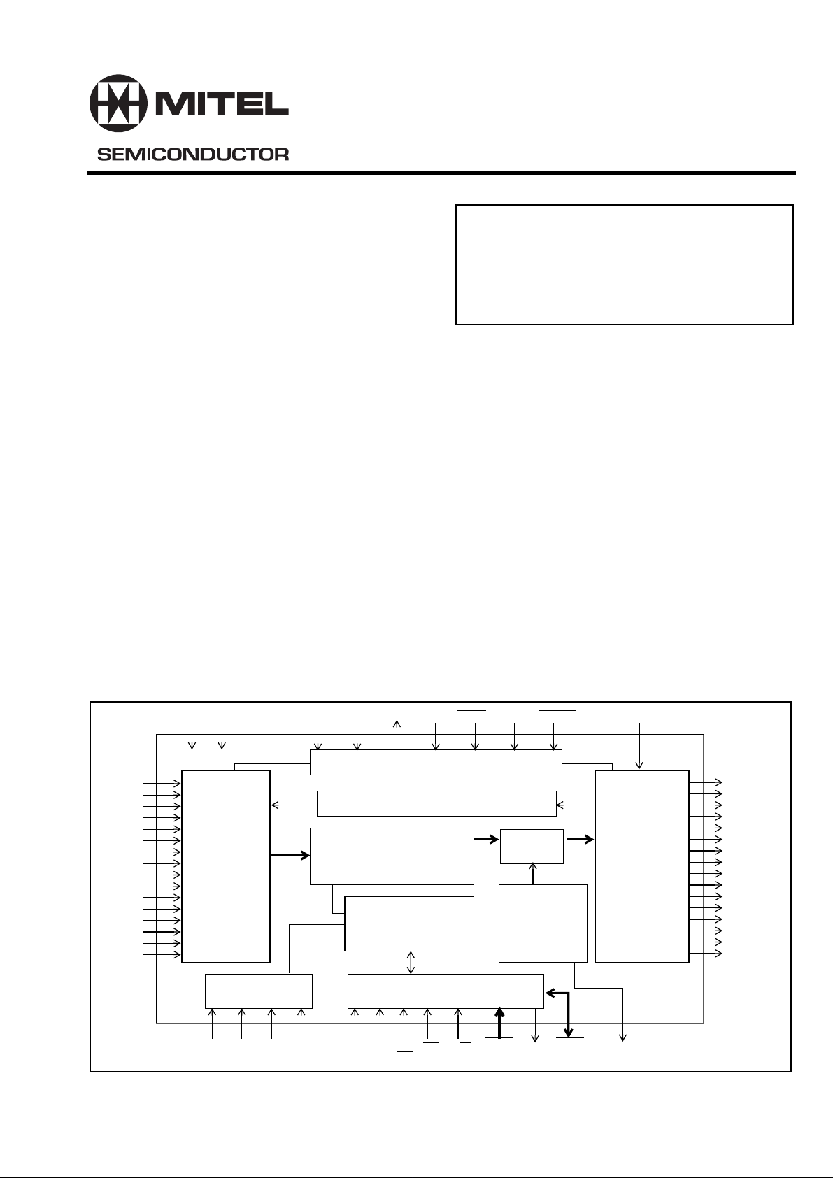
Figure 1 - Functional Block Diagram
Test Port
Loopback
Internal
Registers
Microprocessor Interface
RD
CS R/W
/WR
A7-A0
Output
MUX
Connection
Memory
D15-D8/
DTA
AD7-AD0
ODE
Parallel
to
Serial
Converter
CSTo
STo0
STo1
STo2
STo3
STo4
STo5
STo6
STo7
STo8
STo9
STo10
STo11
STo12
STo13
STo14
STo15
1
Page 2
MT90823 CMOS
STi0
STi1
STi2
STi3
STi4
STi5
STi6
STi7
STi8
STi9
STi10
STi11
STi12
STi13
STi14
STi15
F0i
FE/HCLK
VSS
CLK
VDD
ODE
STo0
STo1
STo2
STo3
STo4
STo5
STo6
STo7
VSS
VDD
STo8
STo9
STo10
STo11
STo12
STo13
STo14
STo15
VSS
10
8 6 4 2 84 82 80 78 76
13
15
17
19
21
23
25
27
29
31 55
34
36 38 40 42 44 46 48 50 52
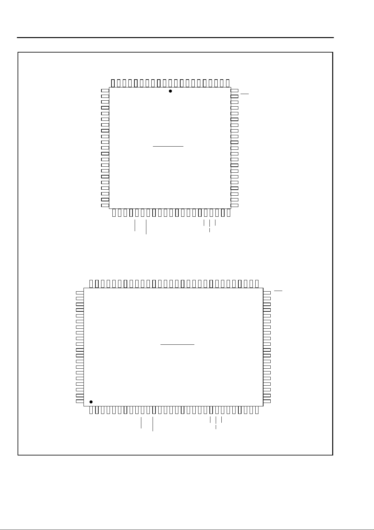
84 PIN PLCC
VSS
CSTo
DTA
73
D15
D14
71
D13
D12
69
D11
D10
67
D9
D8
65
VSS
63
VDD
AD7
61
AD6
AD5
59
AD4
AD3
57
AD2
AD1
AD0
VSS
STi0
STi1
STi2
STi3
STi4
STi5
STi6
STi7
STi8
STi9
STi10
STi11
STi12
STi13
STi14
STi15
F0i
FE/HCLK
VSS
CLK
TDO
STo14
IC
TCK
TRST
WFPS
RESET
VSS
VDD
STo8
STo9
STo10
STo11
STo12
STo13
100 PIN MQFP
(14mm x 20mm x 2.75mm)
DS/RD
STo2
STo3
STo4
STo5
STo6
STo7
22 24 26 28 30
2018161412108642
TDI
TMS
STo15
NC
NC
NC
VSS
NC
82
84
86
88
90
92
94
96
98
99
A7
A6
A5
A4
A3
A2
A1
A0
IM
CS
W/RW
AS/ALE
R/
ODE
STo0
STo1
VSS
NC
NC
NC
CSTo
NC
525456586062646668707274767880
50
DTA
D15
48
D14
D13
46
D12
D11
44
D10
D9
42
D8
VSS
40
VDD
AD7
38
AD6
AD5
36
AD4
AD3
34
AD2
AD1
32
AD0
VSS
NC
NC
NC
NC
VDD
TMS
TDI
TDO
TCK
IC
TRST
WFPS
RESET
A0
A1
A2
A3
A4
A5
A6
A7
RD
DS/
IM
CS
NCNCNC
W/RW
AS/ALE
R/
NC
Figure 2 - PLCC and MQFP Pin Connections
2
Page 3
CMOS MT90823
1
A
B
C
D
E
F
G
H
J
12345678910111213
VSS
VSS
STi0
STi2
STi4
VSS
VSS
STi1
STi3
STi5
STo12
STo14
STo13
STo15
VSS VSSVDD
VDD
VSS
STo11
STo9STo10
STo8
VDD
STo7
VSS
STo6
STo4STo5
STo3
STo2
STo1
VDD
STo0
ODE
VSSVSS VSSVDD
VDD
VSS
VSS
DTA
D14
D12
VSSVSS
VSS
CSTo
D15
D13
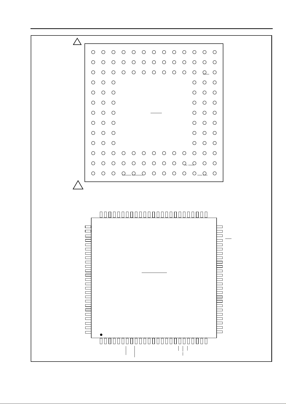
TOP VIEW
VDD
STi6
STi7
VDD
D10
D11
PBGA
VSS
VDD
VSS
D8
AD6
AD4
D9
AD7
AD5
STi8
STi10
STi12
STi9
STi11
STi13
VSS
VDD
VSS
(23mm x 23mm x 2.13mm)
(Ball Pitch = 1.5mm)
K
VDD
STi14
STi15
VDD
AD2
AD3
L
F0i
FE/HCLK
VSS
VDDVDDVDDVDD VSS VSS
VSS
AD0VSS
AD1
M
VSS
VSS
TDI
WFPS
A1
A4
A6
R/W/RW
AS/ALETCK
VSS
VSS
N
CLK
TDO A7
TMS
TRSTICRESET
A0
A2
A5A3
CSDS/RD IM
1 - A1 corner is identified by metallized markings.
NC
NC
STi0
STi1
STi2
STi3
STi4
STi5
STi6
STi7
STi8
STi9
STi10
STi11
STi12
STi13
STi14
STi15
F0i
FE/HCLK
VSS
CLK
VDD
NC
NC
76
78
80
82
84
86
88
90
92
94
96
98
100
NC
NC
VSS
STo15
STo14
STo13
STo12
(14mm x 14mm x 1.4mm)
4 6 8 101214 161820 2224
2
STo8
STo9
STo10
STo11
100 PIN LQFP
(Pin Pitch = 0.50mm)
VDD
VSS
STo7
VSS
NC
5456586062646668707274
52
50
NC
NC
ODE
STo0
STo1
STo2
STo3
STo4
STo5
STo6
NC
CSTo
48
DTA
D15
46
D14
D13
44
D12
42
D11
D10
D9
40
D8
VSS
38
VDD
36
AD7
AD6
34
AD5
AD4
32
AD3
AD2
30
AD1
AD0
28
VSS
NC
26
NC
NC
NC
TMS
TDI
TDO
TCK
IC
TRST
WFPS
RESET
A0
A1
A2
A3
A4
A5
A6
A7
RD
DS/
IM
CS
W/RW
AS/ALE
R/
Figure 3 - PBGA and LQFP Pin Connections
NC
NC
3
Page 4

MT90823 CMOS
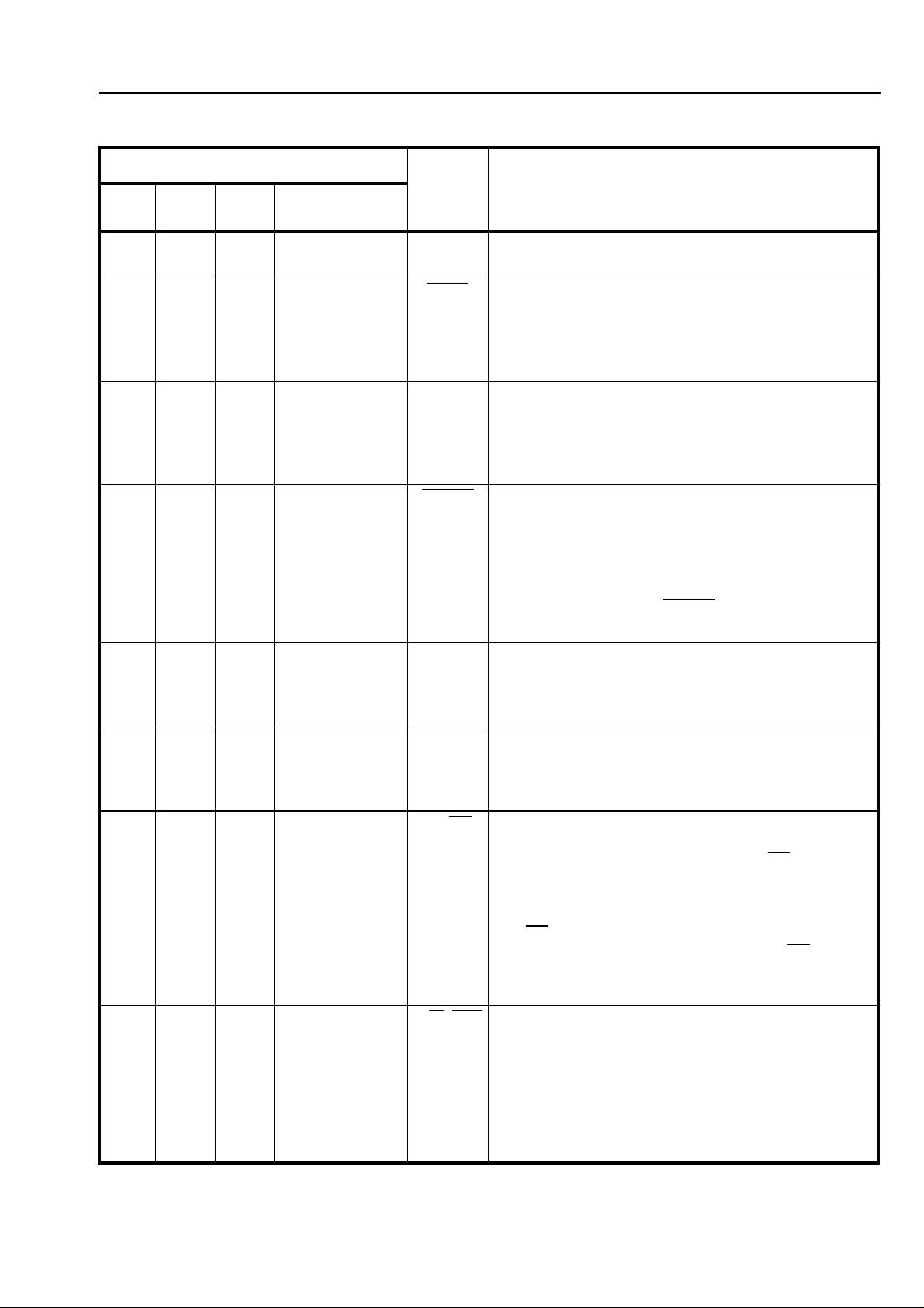
Pin Description
Pin #
84
PLCC
100
MQFP
100
LQFP
120
BGA
Name Description
1, 11,
30, 54
64, 75
2, 32,635, 40,6737,
3 - 10 68-75 65 -72B6,A6,A5,B5,A4,
12 -2781-96 78 -93C1,C2,D1,D2,E1,
31, 41,
56, 66,
76, 99
28 97 94 L1 F0i Frame Pulse (5V Tolerant Input): When the WFPS
28,
38,
53,
63,
73,
96
64,98
A1,A2,A12,A13,
B1,B2,B7,B12,
B13,C3,C5,C7,
C9,C11,E3,E11
G3,G11,J3,J11,
L3,L5,L7,L9,L11,
M2,M12,M13,N1
C4,C6,C8,C10,
D3,D11,F3,F11,
H3,H11,K3,K11,
L4,L6,L8,L10
B4,A3,B3
E2,F1,F2,G1,G2,
H1,H2,J1,J2,K1,
K2
V
SS
V
DD
STo8 - 15 ST-BUS Output 8 to 15 (5V Tolerant Three-state
STi0 - 15 ST-BUS Input 0 to 15 (5V Tolerant Inputs): Serial
Ground.
+3.3 Volt Power Supply.
Outputs): Serial data Output stream. These streams
may have data rates of 2.048, 4.096 or 8.192 Mb/s,
depending upon the value programmed at bits DR0 - 1
in the IMS register.
data input stream. These streams may have data rates
of 2.048, 4.096 or 8.192 Mb/s, depending upon the
value programmed at bits DR0 - 1 in the IMS register.
pin is low, this input accepts and automatically
identifies frame synchronization signals formatted
according to ST-BUS and GCI specifications. When the
WFPS pin is high, this pin accepts a negative frame
pulse which conforms to WFPS formats.
29 98 95 L2 FE/HCLK Frame Evaluation / HCLK Clock (5V Tolerant Input):
When the WFPS pin is low, this pin is the frame
measurement input. When the WFPS pin is high, the
HCLK (4.096MHz clock) is required for frame alignment
in the wide frame pulse (WFP) mode.
31 100 97 N1 CLK Clock (5V T olerant Input):Serial clock for shifting data
in/out on the serial streams (STi/o 0 - 15). Depending
upon the value programmed at bits DR0 - 1 in the IMS
register, this input accepts a 4.096, 8.192 or 16.384
MHz clock.
33 6 3 N2 TMS Test Mode Select (3.3V Input with internal pull-up):
JTAG signal that controls the TAP controller state
transitions.
34 7 4 M3 TDI Test Serial Data In (3.3V Tolerant Input with internal
pull-up): JTAG serial test instructions and data are
shifted in on this pin.
35 8 5 N3 TDO Test Serial Data Out (3.3V Output): JTAG serial data
is output on this pin on the falling edge of TCK. This pin
is held in high impedance state when JTAG scan is not
enabled.
4
Page 5
CMOS MT90823
Pin Description (continued)
Pin #
84
PLCC
36 9 6 M4 TCK Test Clock (5V Tolerant Input): Provides the clock to
37 10 7 N4 TRST Test Reset (3.3V Input with internal pull-up):
38 11 8 M5 IC Internal Connection (3.3V Input with internal
39 12 9 N5 RESET Device Reset (5V Tolerant Input): This input (active
100
MQFP
100
LQFP
120
BGA
Name Description
the JTAG test logic.
Asynchronously initializes the JTAG TAP controller by
putting it in the Test-Logic-Reset state. This pin should
be pulsed low on power-up, or held low, to ensure that
the MT90823 is in the normal functional mode.
pull-down): Connect to VSS for normal operation. This
pin must be low for the MT90823 to function normally
and to comply with IEEE 1149 (JTAG) boundary scan
requirements.
LOW) puts the MT90823 in its reset state to clear the
device internal counters, registers and bring STo0 - 15
and microport data outputs to a high impedance state.
The time constant for a power up reset circuit must be a
minimum of five times the rise time of the power supply.
In normal operation, the RESET pin must be held low
for a minimum of 100nsec to reset the device.
40 13 10 M6 WFPS Wide Frame Pulse Select (5V Tolerant Input): When
1, enables the wide frame pulse (WFP) Frame
Alignment interface. When 0, the device operates in
ST-BUS/GCI mode.
41 -4814-21 11 -
18
49 22 19 N11 DS/RD Data Strobe / Read (5V Tolerant Input): For Motorola
50 23 20 M10 R/W / WR Read/Write / Write (5V Tolerant Input): In the cases
N6,M7,N7,N8,
M8,N9,M9,N10
A0 - A7 Address 0 - 7 (5V Tolerant Input): When
non-multiplexed CPU bus operation is selected, these
lines provide the A0 - A7 address lines to the internal
memories.
multiplexed bus operation, this input is DS. This active
high DS input works in conjunction with CS to enable
the read and write operations.
For Motorola non-multiplexed CPU bus operation, this
input is DS. This active low input works in conjunction
with CS to enable the read and write operations.
For multiplexed bus operation, this input is RD. This
active low input sets the data bus lines (AD0-AD7,
D8-D15) as outputs.
of Motorola non-multiplexed and multiplexed bus
operations, this input is R/W. This input controls the
direction of the data bus lines (AD0 - AD7, D8-D15)
during a microprocessor access.
For multiplexed bus operation, this input is WR. This
active low input is used with RD to control the data bus
(AD0 - 7) lines as inputs.
5
Page 6

MT90823 CMOS
Pin Description (continued)
Pin #
84
PLCC
51 24 21 N12 CS Chip Select (5V T olerant Input):Active low input used
52 25 22 M11 AS/ALE Address Strobe or Latch Enable (5V T olerant Input):
53 26 23 N13 IM CPU Interface Mode (5V Tolerant Input): When IM is
100
MQFP
100
LQFP
120
BGA
Name Description
by a microprocessor to activate the microprocessor
port of MT90823.
This input is used if multiplexed bus operation is
selected via the IM input pin. For Motorola
non-multiplexed bus operation, connect this pin to
ground.
high, the microprocessor port is in the multiplexed
mode. When IM is low, the microprocessor port is in
non-multiplexed mode.
55 -6232-39 29 -
36
65 -7242-49 39 -
46
73 50 47 C12 DTA Data Transfer Acknowledgement (5V tolerant
74 55 48 C13 CST o Control Output (5V Tolerant Output).This is a 4.096,
76 57 54 B11 ODE Output Drive Enable (5V Tolerant Input): This is the
L12,L13,K12,
K13,J12,J13,
H12,H13
G12,G13,F12,
F13,E12,E13,
D12,D13
AD0 - 7 Address/Data Bus 0 to 7 (5V Tolerant I/O): These
pins are the eight least significant data bits of the
microprocessor port. In multiplexed mode, these pins
are also the input address bits of the microprocessor
port.
D8 - 15 Data Bus 8-15 (5V Tolerant I/O): These pins are the
eight most significant data bits of the microprocessor
port.
Three-state Output): Indicates that a data bus transfer
is complete. When the bus cycle ends, this pin drives
HIGH and then tri-states, allowing for faster bus cycles
with a weaker pull-up resistor. A pull-up resistor is
required to hold a HIGH level when the pin is tri-stated.
8.192 or 16.384 Mb/s output containing 512, 1024 or
2048 bits per frame respectively. The level of each bit is
determined by the CSTo bit in the connection memory.
See External Drive Control Section.
output enable control for the STo0-15 serial outputs.
When ODE input is low and the OSB bit of the IMS
register is low, STo0-15 are in a high impedance state.
If this input is high, the STo0-15 output drivers are
enabled. However, each channel may still be put into a
high impedance state by using the per channel control
bit in the connection memory.
77 -8458-65 55 -62A11,B10,A10,B9,
A9,A8,B8,A7
6
STo0 - 7 Data Stream Output 0 to 7 (5V Tolerant Three-state
Outputs): Serial data Output stream. These streams
have selectable data r ates of 2.048, 4.096 or 8.192 Mb/
s.
Page 7
Pin Description (continued)
Pin #
84
PLCC
100
MQFP
100
LQFP
120
BGA
CMOS MT90823
Name Description
- 1 - 4,
27 -
30,
51 -
54
77 -
80
1 - 2,
24 -
27,
49 -
52,
74 -
77,
99 -
100
NC No connection.
Device Overview
The MT90823 Large Digital Switch is capable of
switching up to 2,048 × 2,048 channels. The
MT90823 is designed to switch 64 kb/s PCM or N x
64 kb/s data. The device maintains frame integrity in
data applications and minimum throughput delay for
voice applications on a per channel basis.
The serial input streams of the MT90823 can have a
bit rate of 2.048, 4.096 or 8.192 Mbit/s and are
arranged in 125µs wide frames, which contain 32, 64
or 128 channels, respectively. The data rates on
input and output streams are identical.
By using Mitel’s message mode capability, the
microprocessor can access input and output
time-slots on a per channel basis. This feature is
useful for transferring control and status information
for external circuits or other ST-BUS devices. The
MT90823 automatically identifies the polarity of the
frame synchronization input signal and configures its
serial streams to be compatible to either ST-BUS or
GCI formats.
Two different microprocessor bus interfaces can be
selected through the Input Mode pin (IM):
Non-multiplexed or Multiplexed. These interfaces
provide compatibility with multiplexed and Motorola
multiplexed/non-multiplexed buses.
The frame offset calibration function allows users to
measure the frame offset delay using a frame
evaluation pin (FE). The input offset delay can be
programmed for individual streams using internal
frame input offset registers, see Table 11.
The internal loopback allows the ST-BUS output data
to be looped around to the ST-BUS inputs for
diagnostic purposes.
Functional Description
A functional Block Diagram of the MT90823 is shown
in Figure 1.
Data and Connection Memory
For all data rates, the received serial data is
converted to parallel format by internal
serial-to-parallel converters and stored sequentially
in the data memory. Depending upon the selected
operation programmed in the interface mode select
(IMS) register, the useable data memory may be as
large as 2,048 bytes. The sequential addressing of
the data memory is performed by an internal counter,
which is reset by the input 8 kHz frame pulse (F0i) to
mark the frame boundaries of the incoming serial
data streams.
Data to be output on the serial streams may come
from either the data memory or connection memory.
Locations in the connection memory are associated
with particular ST-BUS output channels. When a
channel is due to be transmitted on an ST-BUS
output, the data for this channel can be switched
either from an ST-BUS input in connection mode, or
from the lower half of the connection memory in
message mode. Data destined for a particular
channel on a serial output stream is read from the
data memory or connection memory during the
previous channel time-slot. This allows enough time
for memory access and parallel-to-serial conversion.
Connection and Message Modes
In the connection mode, the addresses of the input
source data for all output channels are stored in the
connection memory. The connection memory is
mapped in such a way that each location
corresponds to an output channel on the output
7
Page 8

MT90823 CMOS
streams. For details on the use of the source
address data (CAB and SAB bits), see Table 13 and
Table 14. Once the source address bits are
programmed by the microprocessor, the contents of
the data memory at the selected address are
transferred to the parallel-to-serial converters and
then onto an ST-BUS output stream.
By having several output channels connected to the
same input source channel, data can be broadcasted
from one input channel to several output channels.
In message mode, the microprocessor writes data to
the connection memory locations corresponding to
the output stream and channel number. The lower
half (8 least significant bits) of the connection
memory content is transferred directly to the
parallel-to-serial converter. This data will be output
on the ST-BUS streams in every frame until the data
is changed by the microprocessor.
The five most significant bits of the connection
memory controls the following for an output channel:
message or connection mode; constant or variable
delay; enables/tristate the ST-BUS output drivers;
and, enables/disable the loopback function. In addition, one of these bits allows the user to control the
CSTo output.
The MT90823 provides two different interface timing
modes controlled by the WFPS pin. If the WFPS pin
is low, the MT90823 is in ST-BUS/GCI mode. If the
WFPS pin is high, the MT90823 is in the wide frame
pulse (WFP) frame alignment mode.
In ST-BUS/GCI mode, the input 8 kHz frame pulse
can be in either ST-BUS or GCI format. The
MT90823 automatically detects the presence of an
input frame pulse and identifies it as either ST-BUS
or GCI. In ST-BUS format, every second falling edge
of the master clock marks a bit boundary and the
data is clocked in on the rising edge of CLK, three
quarters of the way into the bit cell, see Figure 11. In
GCI format, every second rising edge of the master
clock marks the bit boundary and data is clocked in
on the falling edge of CLK at three quarters of the
way into the bit cell, see Figure 12.
Wide Frame Pulse (WFP) Frame Alignment
Timing
When the device is in WFP frame alignment mode,
the CLK input must be at 16.384 MHz, the FE/HCLK
input is 4.096 MHz and the 8 kHz frame pulse is in
ST-BUS format. The timing relationship between
CLK, HCLK and the frame pulse is defined in Figure
13.
If an output channel is set to a high-impedance state
through the connection memory, the ST-BUS output
will be in a high impedance state for the duration of
that channel. In addition to the per-channel control,
all channels on the ST-BUS outputs can be placed in
a high impedance state by either pulling the ODE
input pin low or programming the output standby
(OSB) bit in the interface mode selection register to
low. This action overrides the individual per-channel
programming by the connection memory bits.
The connection memory data can be accessed via
the microprocessor interface through the D0 to D15
pins. The addressing of the device internal registers,
data and connection memories is performed through
the address input pins and the Memory Select (MS)
bit of the control register. For details on device
addressing, see Software Control and Control
Register bits description (Tables 4, 6 and 7).
Serial Data Interface Timing
The master clock frequency must always be twice
the data rate. The master clock (CLK) must be either
at 4.096, 8.192 or 16.384 MHz for serial data rate of
2.048, 4.096 or 8.192 Mb/s respectively. The input
and output stream data rates will always be identical.
When the WFPS pin is high, the frame alignment
evaluation feature is disabled, but the frame input
offset registers may still be programmed to
compensate for the varying frame delays on the
serial input streams.
Switching Configurations
The MT90823 maximum non-blocking switching
configurations is determined by the data rates
selected for the serial inputs and outputs. The
switching configuration is selected by two DR bits in
the IMS register. See Table 8 and Table 9.
2.048 Mb/s Serial Links (DR0=0, DR1=0)
When the 2.048 Mb/s data rate is selected, the
device is configured with 16-input/16-output data
streams each having 32 64 kb/s channels. This
mode requires a CLK of 4.094 MHz and allows a
maximum non-blocking capacity of 512 x 512
channels.
4.096 Mb/s Serial Links (DR0=1, DR1=0)
When the 4.096 Mb/s data rate is selected, the
device is configured with 16-input/16-output data
streams each having 64 64 kb/s channels. This
8
Page 9

CMOS MT90823
mode requires a CLK of 8.192 MHz and allows a
maximum non-blocking capacity of 1,024 x 1,024
channels.
8.192 Mb/s Serial Links (DR0=0, DR1=1)
When the 8.192 Mb/s data rate is selected, the
device is configured with 16-input/16-output data
streams each having 128 64 kb/s channels. This
mode requires a CLK of 16.384 MHz and allows a
maximum non-blocking capacity of 2,048 x 2,048
channels. Table 1 summarizes the switching
configurations and the relationship between different
serial data rates and the master clock frequencies.
Serial
Interface
Data Rate
2 Mb/s 4.096 512 x 512
4 Mb/s 8.192 1,024 x 1,024
8 Mb/s 16.384 2,048 x 2,048
Table 1- Switching Configuration
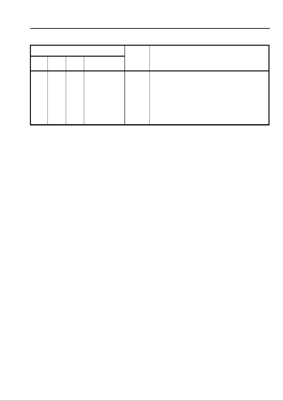
Input Frame Offset Selection
Input frame offset selection allows the channel
alignment of individual input streams to be offset with
respect to the output stream channel alignment (i.e.
F0i). This feature is useful in compensating for
variable path delays caused by serial backplanes of
variable lengths, which may be implemented in large
centralized and distributed switching systems.
Master Clock
Required
(MHz)
Matrix
Channel
Capacity
The SFE bit must be set to zero before starting a
new measurement cycle.
In ST-BUS mode, the falling edge of the frame
measurement signal (FE) is evaluated against the
falling edge of the ST-BUS frame pulse. In GCI
mode, the rising edge of FE is evaluated against the
rising edge of the GCI frame pulse. See Table 10 and
Figure 3 for the description of the frame alignment
register.
This feature is not available when the WFP Frame
Alignment mode is enabled (i.e., when the WFPS pin
is connected to VDD).
Memory Block Programming
The MT90823 provides users with the capability of
initializing the entire connection memory block in two
frames. Bits 11 to 15 of every connection memory
location will be programmed with the pattern stored
in bits 5 to 9 of the IMS register.
The block programming mode is enabled by setting
the memory block program (MBP) bit of the control
register high. When the block programming enable
(BPE) bit of the IMS register is set to high, the block
programming data will be loaded into the bits 11 to
15 of every connection memory location. The other
connection memory bits (bit 0 to bit 10) are loaded
with zeros. When the memory block programming is
complete, the device resets the BPE bit to zero.
Loopback Control
Each input stream can have its own delay offset
value by programming the frame input offset (FOR)
registers. Possible adjustment can range up to +4
master clock (CLK) periods forward with resolution of
1/2 clock period. The output frame offset cannot be
offset or adjusted. See Figure 4, Table 11 and Table
12 for delay offset programming.
Serial Input Frame Alignment Evaluation
The MT90823 provides the frame evaluation (FE)
input to determine different data input delays with
respect to the frame pulse F0i.
A measurement cycle is started by setting the start
frame evaluation (SFE) bit low for at least one frame.
Then the evaluation starts when the SFE bit in the
IMS register is changed from low to high. Two frames
later, the complete frame evaluation (CFE) bit of the
frame alignment register (FAR) changes from low to
high. This signals that a valid offset measurement is
ready to be read from bits 0 to 11 of the FAR register.
The loopback control (LPBK) bit of each connection
memory location allows the ST-BUS output data to
be looped backed internally to the ST-BUS input for
diagnostic purposes.
If the LPBK bit is high, the associated ST-BUS output
channel data is internally looped back to the ST-BUS
input channel (i.e., data from STon channelm routes
to the STi n channelm internally); if the LPBK bit is
low, the loopback feature is disabled. For proper
per-channel loopback operation, the contents of
frame delay offset registers must be set to zero.
Delay Through the MT90823
The switching of information from the input serial
streams to the output serial streams results in a
throughput delay. The device can be programmed to
perform time-slot interchange functions with different
throughput delay capabilities on a per-channel basis.
For voice application, select variable throughput
9
Page 10
MT90823 CMOS
delay to ensure minimum delay between input and
output data. In wideband data applications, select
constant throughput delay to maintain the frame
integrity of the information through the switch.
The delay through the device varies according to the
type of throughput delay selected in the V/C bit of the
connection memory.
Variable Delay Mode (V/C bit = 0)
The delay in this mode is dependent only on the
combination of source and destination channels. It is
independent of input and output streams. The
minimum delay achievable in the MT90823 is three
time-slots. When the input channel data is switched
to the same output channel (channel n, frame p), it
will be output in the following frame (channel n,
frame p+1). The same frame delay occurs if the input
channel n is switched to output channel n+1 or n+2.
When input channel n is switched to output channel
n+3, n+4,..., the new output data will appear in the
same frame. Table 2 shows the possible delays for
the MT90823 in the variable delay mode.
Constant Delay Mode (V/C bit = 1)
In this mode, frame integrity is maintained in all
switching configurations by using a multiple data
memory buffer. Input channel data written into the
data memory buffers during frame n will be read out
during frame n+2.
In the MT90823, the minimum throughput delay
achievable in the constant delay mode is one frame.
For example, in 2 Mb/s mode, when input time-slot
31 is switched to output time-slot 0. The maximum
delay of 94 time-slots occurs when time-slot 0 in a
frame is switched to time-slot 31 in the frame. See
Table 3.
Microprocessor Interface
The MT90823 provides a parallel microprocessor
interface for non-multiplexed or multiplexed bus
structures. This interface is compatible with Motorola
non-multiplexed and multiplexed buses.
If the IM pin is low, the MT90823 microprocessor
interface assumes Motorola non-multiplexed bus
mode. If the IM pin is high, the device microprocessor interface accepts two different timing
modes (mode1 and mode2) which allows direct
connection to multiplexed microprocessors.
The microprocessor interface automatically identifies
the type of microprocessor bus connected to the
MT90823. This circuit uses the level of the DS/RD
input pin at the rising edge of AS/ALE to identify the
appropriate bus timing connected to the MT90823. If
DS/RD is high at the falling edge of AS/ALE, then the
mode 1 multiplexed timing is selected. If DS/RD is
low at the falling edge of AS/ALE, then the mode 2
multiplexed bus timing is selected.
10
Delay for Variable Throughput Delay Mode
(m - output channel number)
Input Rate
m < n m = n, n+1, n+2 m > n+2
2.048 Mb/s 32 - (n-m) time-slots m-n + 32 time-slots m-n time-slots
4.096 Mb/s 64 - (n-m) time-slots m-n + 64 time-slots m-n time-slots
8.192 Mb/s 128 - (n-m) time-slots m-n + 128 time-slots m-n time-slots
Table 2 - Variable Throughput Delay Value
Input Rate
2.048 Mb/s 32 + (32 - n) + (m - 1) time-slots
4.096 Mb/s 64 + (64 - n) + (m- 1) time-slots
8.192 Mb/s 128 + (128 - n) + (m- 1) time-slots
Table 3 - Constant Throughput Delay Value
(n - input channel number))
Delay for Constant Throughput Delay Mode
(m - output channel number)
(n - input channel number))
Page 11

CMOS MT90823
For multiplexed operation, the 8-bit data and address
(AD0-AD7), 8-bit Data (D8-D15), Address strobe/
Address latch enable (AS/ALE), Data strobe/Read
(DS/RD), Read/Write /Write (R/W/WR), Chip select
(CS) and Data transfer acknowledge (DTA) signals
are required. See Figure 13 and Figure 14 for
multiplexed parallel microport timing.
For the Motorola non-multiplexed bus, the 16-bit data
bus (AD0-AD7, D8-D15), 8-bit address bus (A0-A7)
and 4 control lines (CS, DS, R/W and DTA) signals
are required. See Figure 15 for Motorola nonmultiplexed microport timing.
The MT90823 microport provides access to the
internal registers, connection and data memories. All
locations provide read/write access except for the
data memory and the frame alignment register which
are read only.
Memory Mapping
The address bus on the microprocessor interface
selects the MT90823 internal registers and memory.
If the A7 address input is low, then the control (CR),
interface mode selection (IMS), frame alignment
(FAR) and frame input offset (FOR) registers are
addressed by A6 to A0 as shown in Table 4.
If the A7 address input is high, then the remaining
address input lines are used to select up to 128
memory subsection locations. The number selected
corresponds to the maximum number of channels
per input or output stream. The address input lines
and the stream address bits (STA) of the control
register allow access to the entire data and
connection memories.
The control and IMS registers together control all the
major functions of the device. The IMS register
should be programmed immediately after system
power-up to establish the desired switching
configuration (see “Serial Data Interface Timing”
and “Switching Configurations” ).
an internal memory subsections corresponding to
input or output ST-BUS streams.
The data in the IMS register consists of block
programming bits (BPD0-BPD4), block programming
enable bit (BPE), output standby bit (OSB), start
frame evaluation bit (SFE) and data rate selection
bits (DR0, DR1). The block programming and the
block programming enable bits allows users to
program the entire connection memory, (see Memory
Block Programming section). If the ODE pin is low,
the OSB bit enables (if high) or disables (if low) all
ST-BUS output drivers. If the ODE pin is high, the
contents of the OSB bit is ignored and all ST-BUS
output drivers are enabled.
Connection Memory Control
The contents of the CSTo bit of each connection
memory location are output on the CSTo pin once
every frame. The CSTo pin is a 4.096, 8.192 or
16.384 Mb/s output carrying 512, 1,024 or 2,048 bits
respectively. If the CSTo bit is set high, the
corresponding bit on the CSTo output is transmitted
high. If the CSTo bit is low, the corresponding bit on
the CSTo output is transmitted low. The contents of
the CSTo bits of the connection memory are
transmitted sequentially via the CSTo pin and are
synchronous with the data rates on the other ST-BUS
streams.
The CSTo bit is output one channel before the
corresponding channel on the ST-BUS. For example,
in 2Mb/s mode, the contents of the CSTo bit in
position 0 (STo0, CH0) of the connection memor y is
output on the first clock cycle of channel 31 via CSTo
pin. The contents of the CSTo bit in position 32
(STo1, CH0) of the connection memor y is output on
the second clock cycle of channel 31 via CSTo pin.
When either the ODE pin or the OSB bit is high, the
OE bit of each connection memory location enables
(if high) or disables (if low) the output drivers for an
individual ST-BUS output stream and channel. Table
5 details this function.
The control register controls switching operations in
the MT90823. It selects the internal memory
locations that specify the input and output channels
selected for switching.
The data in the control register consists of the
memory block programming bit (MBP), the memory
select bit (MS) and the stream address bits (STA).
The memory block programming bit allows users to
program the entire connection memory block, (see
“Memory Block Programming” ). The memory select
bit controls the selection of the connection memory
or the data Memory. The stream address bits define
The connection memory message channel (MC) bit
(if high) enables message mode in the associated
ST-BUS output channel. When message mode is
enabled, only the lower half (8 least significant bits)
of the connection memory is transferred to the
ST-BUS outputs.
If the MC bit is low, the contents of the connection
memory stream address bit (SAB) and channel
address bit (CAB) defines the source information
(stream and channel) of the time-slot that will be
switched to the output.
11
Page 12

MT90823 CMOS
Bit V/C (Variable/Constant Delay) of each connection
memory location allows the per-channel selection
back to the ST-BUS input channel (i.e., STo
channelm data loops back to STi Nchannelm).
between variable and constant throughput delay
modes.
If the LPBK bit is low, the loopback feature is
disabled. For proper per-channel loopbac k oper ation,
The loopback bit should be used for diagnostic
purpose only; this bit should be set to zero for normal
the contents of the frame delay offset registers must
be set to zero.
operation. If all LPBK bits are set high for all
connection memory locations, the associated
ST-BUS output channel data is internally looped
A7
(Note 1)
A6 A5 A4 A3 A2 A1 A0 Location
0 0 0 0 0 0 0 0 Control Register, CR
0 0 0 0 0 0 0 1 Interface Mode Selection Register, IMS
0 0 0 0 0 0 1 0 Frame Alignment Register, FAR
0 0 0 0 0 0 1 1 Frame Input Offset Register 0, FOR0
0 0 0 0 0 1 0 0 Frame Input Offset Register 1, FOR1
0 0 0 0 0 1 0 1 Frame Input Offset Register 2, FOR2
0 0 0 0 0 1 1 0 Frame Input Offset Register 3, FOR3
N
1
1
1
1
1
1
1
1
1
1
1
1
1
1
1
Notes:
1. Bit A7 must be high for access to data and connection memory positions. Bit A7 must be low for access to registers.
2. Channels 0 to 31 are used when serial interface is at 2Mb/s mode.
3. Channels 0 to 63 are used when serial interface is at 4Mb/s mode.
4. Channels 0 to 127 are used when serial interface is at 8Mb/s mode.
0
0
0
0
0
0
0
0
0
0
1
1
1
1
1
0
0
0
0
0
1
1
1
1
1
0
0
.
1
1
0
0
.
1
1
0
0
.
1
1
0
0
.
1
1
0
0
.
1
1
0
0
.
1
1
0
0
.
1
1
0
0
.
1
1
0
0
.
1
1
0
0
.
1
1
0
0
.
1
1
0
0
.
1
1
0
0
.
1
1
0
Ch 0
1
Ch 1
.
.
0
Ch 30
1
Ch 31 (Note 2)
0
Ch 32
1
Ch 33
.
.
0
Ch 62
1
Ch 63 (Note 3)
0
Ch 64
1
Ch 65
.
.
0
Ch 126
1
Ch 127 (Note 4)
Table 4 - Internal Register and Address Memory Mapping
OE bit in Connection
Memory
ODE pin OSB bit in IMS register ST-BUS Output Driver Status
12
0 Don’t Care Don’t Care Per Channel
High Impedance
1 0 0 High Impedance
1 0 1 Enable
1 1 Don’t care Enable
Table 5 - Output High Impedance Control
Page 13

CMOS MT90823
Initialization of the MT90823
During power up, the TRST pin should be pulsed low,
or held low continuously, to ensure that the MT90863
is in the normal functional mode. A 5K pull-down
resistor can be connected to this pin so that the
device will not enter the JTAG test mode during
power up.
Upon power up, the contents of the connection
memory can be in any state and the ODE pin should
be held low to keep all ST-BUS outputs in a high
impedance state until the microprocessor has
initialized the switching matrix.
Read/Write Address: 00H,
Reset Value: 0000H.
1415
To prevent two ST-BUS outputs from driving the
same stream simultaneously, the microprocessor
should program the desired active paths through the
switch and put all other channels into a high
impedance state during the initialization routine by
using the block programming mode. In addition, the
loopback bits in the connection memory should be
cleared for normal operation.
When this process is complete, the microprocessor
controlling the matrices can bring the ODE pin or
OSB bit high to relinquish the high impedance state
control to the OE bit in the connection memory.
765432108910111213
MSMBP0000000000
STA0STA1STA2STA3
Bit Name Description
15 - 6 Unused Must be zero for normal operation.
5 MBP Memory Block Program. When 1, the connection memory block programming
feature is ready for the prog r amming of Connection Memory high bits, bit 11 to bit 15.
When 0, this feature is disabled.
4MSMemory Select. When 0, connection memory is selected for read or write operations.
When 1, the data memory is selected for read operations and connection memory is
selected for write operations. (No microprocessor write operation is allowed for the
data memory.)
3 - 0 STA3-0 Stream Address Bits. The binary value expressed b y these bits refers to the input or
output data stream, which corresponds to the subsection of memory made accessible
for subsequent operations. (STA3 = MSB, STA0 = LSB)
Table 6 - Control (CR) Register Bits
Input/Output
Data Rate
2.048 Mb/s A4, A3, A2, A1, A0
4.096 Mb/s A5, A4, A3, A2, A1, A0
Valid Address Lines
8.192 Mb/s A6, A5, A4 A3, A2, A1, A0
Table 7 - Valid Address lines for Different Bit Rates
13
Page 14

MT90823 CMOS
Read/Wri
Add
01
te
ress:
Reset Value: 0000H.
,
H
1415
0
0000
BPD
0
4
765432108910111213
32
BPDBPDBPD
BPD
10
BPE OSB SFE
DR0DR1
Bit Name Description
15-10 Unused Must be zero for normal operation.
9-5 BPD4-0 Block Programming Data. These bits carry the value to be loaded into the
connection memory block whenever the memory block programming feature is
activated. After the MBP bit in the control register is set to 1 and the BPE bit is set to
1, the contents of the bits BPD4- 0 are loaded into bit 15 to bit 11 of the connection
memory. Bit 10 to bit 0 of the connection memory are set to 0.
4 BPE Begin Block programming Enable. A zero to one transition of this bit enables the
memory block programming function. The BPE and BPD4-0 bits in the IMS register
have to be defined in the same write operation. Once the BPE bit is set high, the
device requires two frames to complete the block programming. After the
programming function has finished, the BPE bit returns to zero to indicate the
operation is completed. When the BPE = 1, the BPE or MBP can be set to 0 to abort
the programming operation.
When BPE = 1, the other bits in the IMS register must not be changed for two frames
to ensure proper operation.
3 OSB Output standby. When ODE = 0 and OSB = 0, the output drivers of STo0 to STo15
are in high impedance mode. When ODE = 0 and OSB = 1, the output driver of STo0
to STo15 function normally. When ODE = 1, STo0 to STo15 output drivers function
normally.
2 SFE Start Frame Evaluation. A zero to one transition in this bit starts the frame evaluation
procedure. When the CFE bit in the FAR register changes from zero to one, the
evaluation procedure stops . To start another frame evaluation cycle, set this bit to zero
for at least one frame.
1 - 0 DR1-0 Data Rate Select. Input/Output data rate selection. See Table 9 for detailed
programming.
Table 8 - Interface Mode Selection (IMS) Register Bits
DR1 DR0 Data Rate Selected Master Clock Required
0 0 2.048 Mb/s 4.096 MHz
0 1 4.096 Mb/s 8.192 MHz
1 0 8.192 Mb/s 16.384 MHz
1 1 Reserved Reserved
Table 9 - Serial Data Rate Selection (16 input x 16 output)
14
Page 15

CMOS MT90823
Read Add
02
ress:
,
H
Reset Value: 0000H.
1415
0
765432108910111213
Bit Name Description
15 - 13 Unused Must be zero for normal operation.
12 CFE Complete Frame Evaluation. When CFE = 1, the frame evaluation is
completed and bits FD10 to FD0 bits contains a valid frame alignment offset.
This bit is reset to zero, when SFE bit in the IMS register is changed from 1 to
0.
11 FD11 Frame Delay Bit 11. The falling edge of FE (or rising edge for GCI mode) is
sampled during the CLK-high phase (FD11 = 1) or during the CLK-low phase
(FD11 = 0). This bit allows the measurement resolution to 1/2 CLK cycle.
10 - 0 FD10-0 Frame Delay Bits. The binary value expressed in these bits refers to the
measured input offset value. These bits are reset to zero when the SFE bit of
the IMS register changes from 1 to 0. (FD10 = MSB, FD0 = LSB)
Table 10 - Frame Alignment (FAR) Register Bits
FD0FD1FD2FD3FD4FD5FD6FD7FD8FD9FD10FD11CFE00
ST-BUS Frame
CLK
Offset Value
FE Input
GCI Frame
CLK
Offset Value 10 2 3 4 5 6 7 8 9 10 11 12 13 14 15
FE Input
10 2 3 4 5 6 7 8 9 10 11 12 13 14 15 16
(FD[10:0] = 06H)
(FD11 = 0, sample at CLK low phase)
(FD[10:0] = 09
(FD11 = 1, sample at CLK high phase)
)
H
Figure 4 - Example for Frame Alignment Measurement
15
Page 16

MT90823 CMOS
Read/Write Address: 03Hfor FOR0 register,
Reset value: 0000H for all FOR registers.
04H for FOR1 register,
05H for FOR2 register,
06H for FOR3 register,
1415
765432108910111213
OF02
DLE1OF10OF11OF12DLE2OF20OF21OF22DLE3OF30OF31OF32
DLE0OF00OF01
FOR0 register
1415
765432108910111213
OF42
DLE5OF50OF51OF52DLE6OF60OF61OF62DLE7OF70OF71OF72
DLE4OF40OF41
FOR1 register
1415
765432108910111213
OF82
DLE9OF90OF91OF92DLE10OF100OF101OF102DLE11OF110OF111OF112
DLE8OF80OF81
FOR2 register
1415
765432108910111213
OF122
DLE13OF130OF131OF132DLE14OF140OF141OF142DLE15OF150OF151OF152
DLE12OF120OF121
FOR3 register
Name
(Note 1)
Description
OFn2, OFn1, OFn0 Offset Bits 2,1 & 0. These three bits define how long the serial interface receiver takes
to recognize and store bit 0 from the STi input pin: i.e., to start a new frame. The input
frame offset can be selected to +4 clock periods from the point where the external
frame pulse input signal is applied to the F0i input of the device. See Figure 4.
DLEn Data Latch Edge.
ST-BUS mode: DLEn =0, if clock rising edge is at the 3/4 point of the bit cell.
DLEn =1, if when clock falling edge is at the 3/4 of the bit cell.
GCI mode: DLEn =0, if clock falling edge is at the 3/4 point of the bit cell.
DLEn =1, if when clock rising edge is at the 3/4 of the bit cell.
Note 1: n denotes an input stream number from 0 to 15.
Table 11 - Frame Input Offset (FOR) Register Bits
16
Page 17

CMOS MT90823
Input Stream
Measurement Result from
Frame Delay Bits
Corresponding
Offset Bits
Offset
FD11 FD2 FD1 FD0 OFn2 OFn1 OFn0 DLEn
No clock period shift (Default) 1 0 0 0 0000
+ 0.5 clock period shift 0 0 0 0 0001
+1.0 clock period shift 1 0 0 1 0010
+1.5 clock period shift 0 0 0 1 0011
+2.0 clock period shift 1 0 1 0 0100
+2.5 clock period shift 0 0 1 0 0101
+3.0 clock period shift 1 0 1 1 0110
+3.5 clock period shift 0 0 1 1 0111
+4.0 clock period shift 1 1 0 0 1000
+4.5 clock period shift 0 1 0 0 1001
Table 12 - Offset Bits (OFn2, OFn1, OFn0, DLEn) and Frame Delay Bits (FD11, FD2-0)
ST-BUS F0i
CLK
STi Stream
STi Stream
STi Stream
STi Stream
GCI F0i
CLK
Input Stream
Input Stream
Input Stream
Input Stream
Bit 7
Bit 0
Bit 7
Bit 0
Bit 7
Bit 0
Bit 7
Bit 0
offset=0, DLE=0
offset=1, DLE=0
offset=0, DLE=1
offset=1, DLE=1
denotes the 3/4 point of the bit cell
offset=0, DLE=0
offset=1, DLE=0
offset=0, DLE=1
offset=1, DLE=1
denotes the 3/4 point of the bit cell
Figure 5 - Examples for Input Offset Delay Timing
17
Page 18

MT90823 CMOS
765432108910111213
CAB0CAB1CAB2CAB6SAB0 CAB3CAB4CAB5SAB1SAB2SAB3OE
LPBK
14
V/C15MC
CSTo
Bit Name Description
15 LPBK Per Channel Loopback. This bit should be use for diagnostic purpose only.
Set this bit to zero for normal operation. When loopback bit is set for all
memory location, the STi n channel m data comes from STo nchannel m. For
proper per channel loopback operations, set the delay offset register bits
OFn[2:0] to zero for the streams which are in the loopback mode.
14 V/C Variable /Constant Throughput Delay. This bit is used to select between
the variable (low) and the constant delay (high) modes on a per-channel
basis.
13 MC Message Channel. When 1, the contents of the connection memory are
output on the corresponding output channel and stream. Only the lower byte
(bit 7 - bit 0) will be output to the ST-BUS output pins. When 0, the contents of
the connection memory are the data memory address of the switched input
channel and stream.
12 CSTo Contr ol ST-BUS output. This bit is output on the CSTo pin one channel early.
The CSTo bit for stream 0 is output first.
11 OE Output Enable. This bit enables the ST-BUS output drivers on a per-channel
basis.
When 1, the output driver functions normally . When 0, the output driv er is in a
high-impedance state.
10 - 8,
7
SAB3-0 Source Stream Address Bits. The binary value is the number of the data
stream for the source of the connection.
(Note 1)
6 - 0
(Note 1)
Note 1: If bit 13 (MC) of the corresponding connection memory location is 1 (device in message mode), then these entire 8 bits
(SAB0, CAB6 - CAB0) are output on the output channel and stream associated with this location.
CAB6-0 Source Channel Address Bits. The binary value is the number of the
channel for the source of the connection.
Table 13 - Connection Memory Bits
Data Rate CAB Bits Used to Determine the Source Channel of the Connection
2.048 Mb/s CAB4 to CAB0 (32 channel/input stream)
18
4.096 Mb/s CAB5 to CAB0 (64 channel/input stream)
8.192 Mb/s CAB6 to CAB0 (128 channel/input stream)
Table 14 - CAB Bits Programming for Different Data Rates
Page 19

CMOS MT90823
JTAG Support
The MT90823 JTAG interface conforms to the IEEE
1149.1 Boundary-Scan standard and the
Boundary-Scan Test (BST) design-for-testability
technique it specifies. The operation of the
boundary-scan circuitry is controlled by an external
test access port (TAP) Controller.
Test Access Port (TAP)
The Test Access Port (TAP) provides access to the
many test functions of the MT90823. It consists of
three input pins and one output pin. The following
pins comprise the TAP.
• Test Clock Input (TCK)
TCK provides the clock for the test logic. The
TCK does not interfere with any on-chip clock
and thus remains independent. The TCK
permits shifting of test data into or out of the
Boundary-Scan register cells concurrently with
the operation of the device and without
interfering with the on-chip logic.
• Test Mode Select Input (TMS)
The logic signals received at the TMS input are
interpreted by the TAP Controller to control the
test operations. The TMS signals are sampled
at the rising edge of the TCK pulse. This pin is
internally pulled to Vdd when it is not driven
from an external source.
• Test Data Input (TDI)
Serial input data applied to this port is fed
either into the instruction register or into a test
data register, depending on the sequence
previously applied to the TMS input. Both
registers are described in a subsequent
section. The received input data is sampled at
the rising edge of TCK pulses. This pin is
internally pulled to Vdd when it is not driven
from an external source.
• Test Reset (TRST)
Resets the JTAG scan structure. This pin is
internally pulled to VDD.
Instruction Register
In accordance with the IEEE 1149.1 standard, the
MT90823 uses public instructions. The MT90823
JTAG Interface contains a two-bit instruction register.
Instructions are serially loaded into the instruction
register from the TDI when the TAP Controller is in
its shifted-IR state. Subsequently, the instructions
are decoded to achieve two basic functions: to select
the test data register that may operate while the
instruction is current, and to define the serial test
data register path, which is used to shift data
between TDI and DO during data register scanning.
Test Data Register
As specified in IEEE 1149.1, the MT90823 JTAG
Interface contains three test data registers:
• The Boundary-Scan Register
The Boundary-Scan register consists of a
series of Boundary-Scan cells arranged to form
a scan path around the boundary of the
MT90823 core logic.
• The Bypass Register
The Bypass register is a single stage shift
register that provides a one-bit path from TDI to
its TDO.
• The Device Identification Register
The device identification register is a 32-bit
register with the register contain of:
MSB
0000 0000 1000 0010 0011 0001 0100 1011
LSB
• Test Data Output (TDO)
Depending on the sequence previously applied
to the TMS input, the contents of either the
instruction register or data register are serially
shifted out towards the TDO. The data out of
the TDO is clocked on the falling edge of the
TCK pulses. When no data is shifted through
the boundary scan cells, the TDO driver is set
to a high impedance state.
The LSB bit in the device identification register is
the first bit clocked out.
The MT90823 boundary scan register contains 118
bits. Bit 0 in Table 15 Boundary Scan Register is the
first bit clocked out. All tristate enable bits are active
high.
19
Page 20

MT90823 CMOS
Boundary Scan Bit 0 to Bit 117
Device Pin
STo7
STo6
STo5
STo4
STo3
STo2
STo1
STo0
ODE 16
CSTo 17 18
DTA19
D15
D14
D13
D12
D11
D10
D9
D8
AD7
AD6
AD5
AD4
AD3
AD2
AD1
AD0
IM 68
AS/ALE 69
CS 70
R/W / WR 71
DS/RD 72
Tristate
Control
0
2
4
6
8
10
12
14
20
23
26
29
32
35
38
41
44
47
50
53
56
59
62
65
Output
Scan
Cell
1
3
5
7
9
11
13
15
21
24
27
30
33
36
39
42
45
48
51
54
57
60
63
66
Input
Scan
Cell
22
25
28
31
34
37
40
43
46
49
52
55
58
61
64
67
Boundary Scan Bit 0 to Bit 117
Device Pin
A7
A6
A5
A4
A3
A2
A1
A0
WFPS 81
RESET 82
CLK 83
FE/HCLK 84
F0i 85
STi15
STi14
STi13
STi12
STi11
STi10
STi9
STi8
STi7
STi6
STi5
STi4
STi3
STi2
STi1
STi0
STo15
STo14
STo13
STo12
STo11
STo10
STo9
STo8
Tristate
Control
102
104
106
108
110
112
114
116
Output
Scan
Cell
103
105
107
109
111
113
115
117
Input
Scan
Cell
73
74
75
76
77
78
79
80
86
87
88
89
90
91
92
93
94
95
96
97
98
99
100
101
Table 15: Boundary Scan Register Bits
20
Table 15: Boundary Scan Register Bits
Page 21

CMOS MT90823
Applications
Switch Matrix Architectures
The MT90823 is an ideal device for medium to large
size switch matrices where voice and grouped data
channels are transported within the same frame. In
such applications, the voice samples have to be time
interchanged with a minimum delay while maintaining the integrity of grouped data. To ensure the
integrity of grouped data during switching and to
provide a minimum delay for voice connections, the
MT90823 provides per-channel selection between
variable and constant throughput delay. This can be
selected by the V/C bit of the Connection Memory.
16 Streams
IN
16 Streams
MT90823
#1
MT90823
#2
Figure 6 illustrates how four MT90823 devices can
be used to form non-blocking switches for up to 4096
channels with data rate of 8.192 Mb/s.
Serial Input Frame Alignment Evaluation
The MT90823 is capable of performing frame
alignment evaluation. The frame pulse under
evaluation is connected to the FE (frame measurement) pin. An external multiplexer is required to
select one of the frame pulses related to the different
input streams. The block diagram at Figure 7 shows
a switch matrix that performs frame alignment
evaluation for 16 frame pulses.
16 Streams
OUT
16 Streams
MT90823
#3
MT90823
#4
Bit Rate
(IN/OUT)
2.048 Mb/s 1,024 - Channel Switch
4.096 Mb/s 2,048 - Channel Switch
Size of
Switch Matrix
4,096 - Channel Switch8.192 Mb/s
Figure 6 - Switch Matrix with Serial Stream at Various Bit Rates
STi0
STi1
STi2
STi15
External
Mux
FP STi0
FP STi1
FP STi2
FP STi15
Note:
1. Use the external mux to select one of the serial frame pulses.
2. To start a measurement cycle, set the Start Frame Evaluation (SFE) bit in the IMS register low for at least 1 frame.
3. Frame evaluation starts when the SFE bit is changed from low to high.
4. Two frames later, the Complete Frame Evaluation (CFE) bit of the Frame Alignment Register (FAR) changes from low to
high to signal the CPU that a valid offset measurement is ready to be read from bit [11:0] of the FAR register.
5. The SFE bit must be set to zero before a new measurement cycle started.
input
MT90823
Frame Alignment
Evaluation circuit
FE
CLK FP
STo[0:15]
Central
Timing Source
Figure 7 - Serial Input Frame Alignment Evaluation for Various Frame Pulses
21
Page 22

MT90823 CMOS
Wide Frame Pulse (WFP) Frame Alignment
Mode
When the device is in the wide frame pulse mode
and if the input data streams are sampled at 3/4 bit
time, the device can operate in the HMVIP and
MVIP-90 environment. When input data streams are
sampled at half-bit time as specified in the HMVIP
and MVIP-90 standard, the device can only operate
with data rate of 2 Mb/s. Refer to the ST-BUS output
delay parameter, t
, as specified in the AC
SOD
Electrical Characteristic table.
The MT90823 is designed to accept a common
frame pulse F0i, the 4.096 MHz and 16.384 MHz
clocks required by the HMVIP standards. To enable
the Wide Frame Pulse Frame Alignment Mode, the
WFPS pin has to be set to HIGH and the DR1 and
DR0 bits set for 8.192Mb/s data rate operation.
Digital Access Cross-Connect System
Figure 8 illustrates the use of MT90823 devices to
construct a 256 E1/T1 Digital Access Cross- connect
System (DACS). The system consists of 32 trunk
cards each having eight E1 or T1 trunk interfaces for
a total of 256 trunks. Each trunk card uses two
MT8986 Multi-rate Digital Switches. The central
switching block uses 16 MT90823 devices.
x 4,096 channel switch modules. Figure 6 shows the
implementation of the individual 4,096 x 4,096
channel switch modules from four MT90823 devices.
Figure 10 shows an eight-stream trunk card using
MT8986 Multi-rate Digital Switches to concentrate
32-channel 2.048 Mb/s ST-BUS (DSTi and DSTo)
streams at each E1/T1 trunk onto four 128-channel
8.192 Mb/s streams.
The DACS switching matrix that formerly required
256 MT8986 devices in a square (16 x 16)
configuration can now be provided by 64 MT8986
and 16 MT90823 devices (see Figure 8).
The block diagram at Figure 9 shows how an 8,192 x
8,192 channel switch can be constructed from 4,096
Each line represents a stream
that consists of
128 channels at 8.192Mb/s
64 input streams
x
64 output streams
E1
E1
E1
E1
E1
E1
15
247
255
TC0
0
7
8
8 x E1/T1
Trunk Card
TC1
8 x E1/T1
Trunk Card
TC31
8 x E1/T1
Trunk Card
(Figure 10)
8,192 x 8,192 channel
Switch Matrix
Sixteen MT90823
(8 Mb/s mode)
(See Figure 9)
22
Figure 8 - 256 E1/T1 Digital Access Cross-Connect System (DACS)
Page 23

CMOS MT90823
E1
E1
0
1
32 Streams
IN
32 Streams
E1/T1 Trunk 0
E1/T1 Trunk 1
4,096 x 4,096
Switch Matrix
(Figure 6)
4,096 x 4,096
Switch Matrix
(Figure 6)
4,096 x 4,096
Switch Matrix
(Figure 6)
4,096 x 4,096
Switch Matrix
(Figure 6)
Figure 9 - 8,192 x 8,192 Channel Switch Matrix
DSTo
DSTi
DSTo
DSTi
STi0
STi1
STi7
MT8986
2 Mb/s
to
8 Mb/s
STo0
STo1
32 Streams
OUT
32 Streams
256-channel out
(8.192 Mb/s per channel)
E1
STo0
STo1
7
E1/T1 Trunk 7
DSTo
DSTi
STo7
MT8986
8 Mb/s
to
2 Mb/s
STi0
STi1
256-channel in
(8.192 Mb/s per channel)
Figure 10 - Trunk Card Block Diagram
23
Page 24

MT90823 CMOS
Absolute Maximum Ratings*
Parameter Sym Min Max Units
1 Supply Voltage V
2 Voltage on any 3.3V Tolerant pin I/O (other than supply pins) V
3 Voltage on any 5V Tolerant pin I/O (other than supply pins) V
4 Continuous Current at digital outputs I
5 Package power dissipation (PLCC & PQFP) P
6 Storage temperature T
* Exceeding these values may cause permanent damage. Functional operation under these conditions is not implied
DD
I
I
o
D
S
Recommended Operating Conditions - Voltages are with respect to ground (V
-0.3 5.0 V
VSS- 0.3 VDD+ 0.3 V
VSS- 0.3 5.5 V
- 65 +125 °C
) unless otherwise stated.
ss
Characteristics Sym Min Typ Max Units Test Conditions
1 Operating Temperature T
2 Positive Supply V
3 Input High Voltage V
4 Input High Voltage on 5V Tolerant
OP
DD
IH
V
IH
-40 +85 °C
3.0 3.6 V
0.7V
DD
V
DD
5.5 V
V 400mV noise margin
Inputs
5 Input Low Voltage V
DC Electrical Characteristics - Voltages are with respect to ground (V
V
IL
SS
0.3V
DD
) unless otherwise stated.
ss
V 400mV noise margin
Characteristics Sym Min Typ Max Units Test Conditions
20 mA
1W
1
Supply Current
I
N
2 Input High Voltage V
P
U
3 Input Low Voltage V
T
S
4 Input Leakage (input pins)
Input Leakage (with pull-up or
pull-down)
5 Input Pin Capacitance C
6
7 Output Low Voltage V
8 High Impedance Leakage I
9 Output Pin Capacitance C
Note:
1. Maximum leakage on pins (output or I/O pins in high impedance state) is over an applied voltage (V)
Output High Voltage V
O
U
T
P
U
T
S
@ 2 Mb/s
I
@ 4 Mb/s 20 26 mA
DD
12 15 mA
@ 8 Mb/s 45 70 mA
I
I
OZ
IL
BL
OH
OL
0.7V
IH
IL
DD
0.3V
DD
15
50
I
0.8V
DD
10 pF
0.4 V IOL = 10mA
5 µA 0 < V < VDD See
O
10 pF
V
V
µA
µA0≤<V≤VDD See
VIOH = -10mA
Output unloaded
Note 1
Note 1
AC Electrical Characteristics - Timing Parameter Measurement Voltage Levels
Characteristics Sym Level Units Conditions
1 CMOS Threshold V
2 Rise/Fall Threshold Voltage High V
3 Rise/Fall Threshold Voltage Low V
CT
HM
LM
0.5V
0.7V
0.3V
DD
DD
DD
V
V
V
24
Page 25

AC Electrical Characteristics - Frame Pulse and CLK
Characteristic Sym Min Typ Max Units Notes
CMOS MT90823
1 Frame pulse width (ST-BUS, GCI)
Bit rate = 2.048 Mb/s
Bit rate = 4.096 Mb/s
Bit rate = 8.192 Mb/s
2 Frame Pulse Setup time before
CLK falling (ST-BUS or GCI)
3 Frame Pulse Hold Time from CLK
falling (ST-BUS or GCI)
4 CLK Period
Bit rate = 2.048 Mb/s
Bit rate = 4.096 Mb/s
Bit rate = 8.192 Mb/s
5 CLK Pulse Width High
Bit rate = 2.048 Mb/s
Bit rate = 4.096 Mb/s
Bit rate = 8.192 Mb/s
6 CLK Pulse Width Low
Bit rate = 2.048 Mb/s
Bit rate = 4.096 Mb/s
Bit rate = 8.192 Mb/s
7 Clock Rise/Fall Time
8 Wide frame pulse width
Bit rate = 8.192 Mb/s
9 Frame Pulse Setup Time before
HCLK falling
10 Frame Pulse Hold Time from
HCLK falling
11 HCLK (4.096MHz) Period
Bit rate = 8.192 Mb/s
12 HCLK (4.096MHz) Pulse Width
High
Bit rate = 8.192 Mb/s
13 HCLK (4.096MHz) Pulse Width
Low
Bit rate = 8.192 Mb/s
14 HCLK Rise/Fall Time
15 Delay between falling edge of
HCLK and falling edge of CLK
t
FPW
t
FPS
t
FPH
t
t
CH
t
tr, t
t
HFPW
t
HFPS
t
HFPH
t
HCP
t
HCH
t
HCL
tHr, t
t
DIF
CP
CL
26
26
26
295
145
80
ns
ns
ns
WFPS Pin = 0
5 ns WFPS Pin = 0
10 ns WFPS Pin = 0
190
110
55
85
50
20
85
50
20
f
300
150
70
150
75
40
150
75
40
10 ns
ns
ns
ns
ns
ns
ns
ns
ns
ns
WFPS Pin = 0
WFPS Pin = 0
WFPS Pin = 0
195 295 ns WFPS Pin = 1
5 150 ns WFPS Pin = 1
10 150 ns WFPS Pin = 1
190 300 ns WFPS Pin = 1
85 150 ns WFPS Pin = 1
85 150 ns WFPS Pin = 1
Hf
10 ns
-10 10 ns WFPS Pin = 0 or 1
25
Page 26

MT90823 CMOS
AC Electrical Characteristics - Serial Streams for ST-BUS and GCI Backplanes
Characteristic Sym Min Typ Max Units Test Conditions
1 Sti Set-up Time
2 Sti Hold Time
3 Sto Delay - Active to Active
4 STo delay - Active to High-Z t
5 Sto delay - High-Z to Active t
6 Output Driver Enable (ODE)
t
SIS
t
SIH
t
SOD
DZ
ZD
t
ODE
0ns
10 ns
30
40
nsnsCL=30pF
CL=200pF
32 RL=1K, CL=200pF, See Note 1
32 RL=1K, CL=200pF, See Note 1
32 ns RL=1K, CL=200pF, See Note 1
Delay
7 CSTo Output Delay t
Note:
1. High Impedance is measured by pulling to the appropriate rail with RL, with timing corrected to cancel time taken to discharge CL.
t
FPW
F0i
t
FPS
CLK
t
FPH
XCD
t
SOD
t
CP
30
40
t
CH
nsnsCL=30pF
CL=200pF
t
CL
t
r
V
CT
V
HM
V
TT
V
LM
t
f
STo
STi
Note 1:
2.048 Mb/s mode, last channel = ch 31,
4.196 Mb/s mode, last channel = ch 63,
8.192 Mb/s mode, last channel = ch 127.
Bit 0, Last Ch (Note1) Bit 7, Channel 0 Bit 6, Channel 0 Bit 5, Channel 0
Bit 0, Last Ch (Note1)
t
SIS
Bit 7, Channel 0 Bit 6, Channel 0 Bit 5, Channel 0
t
SIH
V
CT
V
CT
Figure 11 - ST-BUS Timing for 2.048 Mb/s and High Speed Serial Interface at 4.096 Mb/s
or 8.192 Mb/s, when WFPS pin = 0.
26
Page 27

t
FPW
CMOS MT90823
F0i
t
FPS
CLK
STo
STi
Bit 7, Last Ch (Note1) Bit 0, Channel 0 Bit 1, Channel 0 Bit 2, Channel 0
Bit 7, Last Ch (Note1)
Note 1:
2Mb/s mode, last channel = ch 31,
4Mb/s mode, last channel = ch 63,
8Mb/s mode, last channel = ch 127
Figure 12 - GCI Timing at 2.048 Mb/s and High Speed Serial Interface
at 4.096 Mb/s or 8.192 Mb/s, when WFPS pin = 0
t
SOD
t
FPH
t
SIS
t
CP
t
SIH
Bit 0, Channel 0 Bit 1, Channel 0 Bit 2, Channel 0
t
CH
V
CT
t
CL
t
r
V
HM
V
CT
V
LM
t
f
V
CT
V
CT
t
HFPW
t
HFPS
t
HFPH
F0i
t
HCP
t
HCL
t
HCH
HCLK
4.096MHz
t
DIF
t
Hr
t
CP
t
CH
t
Hf
t
CL
t
r
CLK
16.384MHz
STo
STi
Bit 1, Ch 127
Bit 1, Ch 127
Bit 0, Ch 127
Bit 0, Ch 127
t
SOD
Bit 7, Ch 0
t
SIS
Bit 7, Ch 0
Bit 6, Ch 0 Bit 5, Ch 0
t
SIH
Bit 6, Ch 0 Bit 5, Ch 0
Bit 4, Ch 0
Bit 4, Ch 0
t
f
Figure 13 - WFP Bus Timing for High Speed Serial Interface (8.192Mb/s), when WFPS pin = 1
Note:
1. High Impedance is measured by pulling to the appropriate rail with RL, with timing corrected to cancel time taken to discharge CL.
V
CT
V
HM
V
CT
V
LM
V
CT
V
CT
V
CT
27
Page 28

MT90823 CMOS
CLK
(ST-BUS or)
V
CT
(WFPS mode)
CLK
(GCI mode)
STo
STo
CSTo
Valid Data
HiZ
t
DZ
t
ZD
t
XCD
V
CT
HiZ
Valid Data
V
CT
V
CT
V
CT
Figure 14 - Serial Output and External Control
V
ODE
STo
HiZ
t
ODE
Valid Data
t
ODE
HiZ
CT
V
CT
Figure 15 - Output Driver Enable (ODE)
28
Page 29

AC Electrical Characteristics - Multiplexed Bus Timing (Mode 1)
Characteristics Sym Min Typ Max Units Test Conditions
CMOS MT90823
1 ALE pulse width t
2 Address setup from ALE falling t
3 Address hold from ALE falling t
4 RD active after ALE falling t
5 Data setup from DTA Low on Read t
6 CS hold after RD/WR t
7 RD pulse width (fast read) t
8 CS setup from RD t
9 Data hold after RD t
ALW
ADS
ADH
ALRD
DDR
CSRW
RW
CSR
DHR
20 ns
3ns
3ns
3ns
5nsC
=150pF
L
5ns
45 ns
0ns
10 20 ns CL=150pF, RL=1K,
Note 1.
10 WR pulse width (fast write) t
11 WR delay after ALE falling t
12 CS setup from WR t
13 Data setup from WR (fast write) t
14 Valid Data Delay on write (slow write) t
15 Data hold after WR inactive t
16 Acknowledgment Delay:
Reading/Writing Registers
Reading/Writing Memory @ 2Mb/s
@ 4Mb/s
@ 8Mb/s
17 Acknowledgment Hold Time t
WW
ALWR
CSW
DSW
SWD
DHW
t
AKD
AKH
45 ns
3ns
0ns
20 ns
122 ns
5ns
43/43
760/750
400/390
220/210
ns
ns
ns
ns
CL=150pF
CL=150pF
CL=150pF
CL=150pF
22 ns CL=150pF, RL=1K,
Note 1.
Note:
1. High Impedance is measured by pulling to the appropriate rail with RL, with timing corrected to cancel time taken to discharge CL.
ALE
AD0-AD7
D8-D15
CS
RD
WR
DTA
t
ALW
HiZ
t
ADS
t
ADH
ADDRESS
t
ALRD
t
CSR
t
CSW
t
ALWR
HiZ
t
SWD
t
AKD
t
DDR
t
t
RW
WW
Figure 16 - Multiplexed Bus Timing (Mode 1)
t
DSW
DATA
t
CSRW
t
DHR
t
DHW
t
AKH
HiZ
V
CT
V
CT
V
CT
V
CT
V
CT
V
CT
29
Page 30

MT90823 CMOS
AC Electrical Characteristics - Multiplexed Bus Timing (Mode 2)
Characteristics Sym Min Typ Max Units Test Conditions
1 AS pulse width t
2 Address setup from AS falling t
3 Address hold from AS falling t
4 Data setup from DTA Low on Read t
5 CS hold after DS falling t
6 CS setup from DS rising t
7 Data hold after write t
8 Data setup from DS -Write (fast
ASW
ADS
ADH
DDR
CSH
CSS
DHW
t
DWS
20 ns
3ns
3ns
5nsC
=150pF
L
0ns
0ns
5ns
20 ns
write)
9 Valid Data Delay on write (slow write) t
10 R/W setup from DS rising t
11 R/W hold after DS falling t
12 Data hold after read t
SWD
RWS
RWH
DHR
60 ns
5ns
10 20 ns CL=150pF, RL=1K,
122 ns
Note 1
13 DS delay after AS falling t
14 Acknowledgment Delay:
Reading/Writing Registers
Reading/Writing Memory @ 2Mb/s
@ 4Mb/s
@ 8Mb/s
15 Acknowledgment Hold Time t
DSH
t
AKD
AKH
10 ns
43/43
760/750
400/390
220/210
ns
ns
ns
ns
22 ns CL=150pF, RL=1K,
CL=150pF
CL=150pF
CL=150pF
CL=150pF
Note 1
Note 1. High Impedance is measured by pulling to the appropriate rail with RL, with timing corrected to cancel time taken to discharge CL.
DS
R/W
AS
AD0-AD7
D8-D15
WR
AD0-AD7
D8-D15
RD
CS
DTA
t
RWS
t
ADH
t
CSS
t
DSH
HiZ
t
SW
HiZ
t
AKD
HiZ
HiZ
t
ASW
t
ADS
ADDRESS
ADDRESS
Figure 17 - Multiplexed Bus Timing (Mode2)
t
DWS
t
DDR
DATA
DATA
t
DHW
t
t
DHR
AKH
t
CSH
t
RWH
V
CT
V
CT
V
CT
V
CT
V
CT
V
CT
V
CT
30
Page 31

CMOS MT90823
AC Electrical Characteristics - Motorola Non-Multiplexed Bus Mode
Characteristics Sym Min Typ Max Units Test Conditions
1 CS setup from DS falling t
2R/W setup from DS falling t
3 Address setup from DS falling t
4 CS hold after DS rising t
5R/W hold after DS rising t
6 Address hold after DS rising t
7 Data setup from DTA Low on Read t
8 Data hold on read t
CSS
RWS
ADS
CSH
RWH
ADH
DDR
DHR
0ns
10 ns
2ns
0ns
2ns
2ns
2nsC
=150pF
L
10 20 ns CL=150pF, RL=1K
Note 1
9 Data setup on write (fast write) t
10 Valid Data Delay on write (slow write) t
11 Data hold on write t
12 Acknowledgment Delay:
Reading/Writing Registers
Reading/Writing Memory @ 2Mb/s
@ 4Mb/s
@ 8Mb/s
13 Acknowledgment Hold Time t
DSW
SWD
DHW
t
AKD
AKH
0ns
122 ns
5ns
43/43
760/750
400/390
220/210
ns
ns
ns
ns
CL=150pF
CL=150pF
CL=150pF
CL=150pF
22 ns CL=150pF, RL=1K,
Note 1
Note:
1. High Impedance is measured by pulling to the appropriate rail with RL, with timing corrected to cancel time taken to discharge CL.
DS
CS
R/W
A0-A7
AD0-AD7
D8-D15
READ
AD0-AD7
D8-D15
WRITE
DTA
t
t
CSS
t
RWS
ADS
t
SWD
VALID ADDRESS
VALID READ DATA
t
DSW
VALID WRITE DATA
t
DDR
t
AKD
t
CSH
t
t
RWH
t
ADH
t
DHR
DHW
t
AKH
V
CT
V
CT
V
CT
V
CT
V
CT
V
CT
V
CT
Figure 18 - Motorola Non-Multiplexed Bus Timing
31
Page 32

Package Outlines
Pin #1 Corner
12345678910111213
A
B
C
D
E
F
G
H
J
K
L
M
N
3.00*45 °
20.00 REF
(4x)
Ø1.00(3X) REF.
20.00 REF
23.00 ± 0.20
1.50
18.00
Ø
0.75 ± 0.15 (169X)
12345678910111213
A
B
C
D
E
F
G
H
J
K
L
M
N
C
Seating Plane
0.56 REF 0.97 REF
30 ° Typ.
B
2.13 ± 0.13
0.60 ± 0.10
Note: All governing dimensions are in millimetres for design purposes
Ball Gate Array
1.50
18.00
A
23.00 ± 0.20
120-BGA 144-BGA 160-BGA
MT90823 MT90863 MT90826
Page 33

Package Outlines
F
D
1
D
H
E
E
1
e: (lead coplanarity)
A
1
I
E
2
Notes:
1) Not to scale
2) Dimensions in inches
3) (Dimensions in millimeters)
4) For D & E add for allowable Mold Protrusion 0.010"
A
G
D
2
Dim
A
A
D/E
D1/E
D2/E
e
F
G
H
I
20-Pin 28-Pin 44-Pin 68-Pin 84-Pin
Min Max Min Max Min Max Min Max Min Max
0.165
(4.20)
0.090
1
(2.29)
0.385
(9.78)
0.350
1
(8.890)
0.290
2
(7.37)
0.026
(0.661)
0.013
(0.331)
0.020
(0.51)
0.180
(4.57)
0.120
(3.04)
0.395
(10.03)
0.356
(9.042)
0.330
(8.38)
0 0.004 0 0.004 0 0.004 0 0.004 0 0.004
0.032
(0.812)
0.021
(0.533)
0.050 BSC
(1.27 BSC)
0.165
(4.20)
0.090
(2.29)
0.485
(12.32)
0.450
(11.430)
0.390
(9.91)
0.026
(0.661)
0.013
(0.331)
0.050 BSC
(1.27 BSC)
0.020
(0.51)
0.180
(4.57)
0.120
(3.04)
0.495
(12.57)
0.456
(11.582)
0.430
(10.92)
0.032
(0.812)
0.021
(0.533)
0.165
(4.20)
0.090
(2.29)
0.685
(17.40)
0.650
(16.510)
0.590
(14.99)
0.026
(0.661)
0.013
(0.331)
0.050 BSC
(1.27 BSC)
0.020
(0.51)
0.180
(4.57)
0.120
(3.04)
0.695
(17.65)
0.656
(16.662)
0.630
(16.00)
0.032
(0.812)
0.021
(0.533)
0.165
(4.20)
0.090
(2.29)
0.985
(25.02)
0.950
(24.130)
0.890
(22.61)
0.026
(0.661)
0.013
(0.331)
0.050 BSC
(1.27 BSC)
0.020
(0.51)
0.200
(5.08)
0.130
(3.30)
0.995
(25.27)
0.958
(24.333)
0.930
(23.62)
0.032
(0.812)
0.021
(0.533)
(4.20)
(2.29)
(30.10)
(29.210)
(27.69)
(0.661)
(0.331)
(0.51)
0.165
0.090
1.185
1.150
1.090
0.026
0.013
0.050 BSC
(1.27 BSC)
0.020
0.200
(5.08)
0.130
(3.30)
1.195
(30.35)
1.158
(29.413)
1.130
(28.70)
0.032
(0.812)
0.021
(0.533)
General-10
Plastic J-Lead Chip Carrier - P-Suffix
Page 34

http://www.mitelsemi.com
World Headquarters - Canada
Tel: +1 (613) 592 2122
Fax: +1 (613) 592 6909
North America Asia/Pacific Europe, Middle East,
Tel: +1 (770) 486 0194 Tel: +65 333 6193 and Africa (EMEA)
Fax: +1 (770) 631 8213 Fax: +65 333 6192 Tel: +44 (0) 1793 518528
Fax: +44 (0) 1793 518581
Information relating to products and services furnished herein by Mitel Corporation or its subsidiaries (collectively “Mitel”) is believed to be reliable. However, Mitel assumes no
liability for errors that may appear in this publication, or for liability otherwise arising from the application or use of any such information, product or service or for any infringement of
patents or other intellectual property rights owned by third parties which may result from such application or use. Neither the supply of such information or purchase of product or
service conveys any license, either express or implied, under patents or other intellectual property rights owned by Mitel or licensed from third parties by Mitel, whatsoever.
Purchasers of products are also hereby notified that the use of product in certain ways or in combination with Mitel, or non-Mitel furnished goods or services may infringe patents or
other intellectual property rights owned by Mitel.
This publication is issued to provide information only and (unless agreed by Mitel in writing) may not be used, applied or reproduced for any purpose nor form part of any order or
contract nor to be regarded as a representation relating to the products or services concerned. The products, their specifications, services and other information appearing in this
publication are subject to change by Mitel without notice. No warranty or guarantee express or implied is made regarding the capability, performance or suitability of any product or
service. Information concerning possible methods of use is provided as a guide only and does not constitute any guarantee that such methods of use will be satisfactory in a specific
piece of equipment. It is the user’s responsibility to fully determine the performance and suitability of any equipment using such information and to ensure that any publication or
data used is up to date and has not been superseded. Manufacturing does not necessarily include testing of all functions or parameters. These products are not suitable for use in
any medical products whose failure to perform may result in significant injury or death to the user. All products and materials are sold and services provided subject to Mitel’s
conditions of sale which are available on request.
M Mitel (design) and ST-BUS are registered trademarks of MITEL Cor poration
Mitel Semiconductor is an ISO 9001 Registered Company
Copyright 1999 MITEL Corporation
All Rights Reserved
Printed in CANADA
TECHNICAL DOCUMENTATION - NOT FOR RESALE
 Loading...