

Page 1
CMOS ST-BUS FAMILY
MT90820
Large Digital Switch (LDX)
Advance Information
Features
• 2,048 channel non-blocking switch
• Maint ains fr ame integri ty on co ncat enate d
channels.
• Per-chan nel s electi on of mi nim um or co nstan t
throughput delay
• Serial s treams a t 2.0 48, 4. 096 or 8.1 92Mb /s
• Frame offset delay measurement
• Program mab le fr ame d elay offs et
• Per-chan nel thre e-stat e cont rol
• Per-chan nel m essa ge mo de
• Control interface compatible to Intel/Motorola
CPUs
• Block pro gramm ing feature for con nec tion
memory
• ST-BUS/MVIP and GCI interfaces
• Test Port compatible to IEEE-1149.1 standard
Applications
• Medium and l arge swi tchi ng platf orm s
• C.O. switches
• CTI application
• Voice/data mult iple xer
• Digital cross connects
• ST-BUS/HMVIP interface functions
ISSUE 1 May 1995
Ordering Information
MT9082 0A P 84 Pin P L CC
MT90820AL 100 Pin QFP
-40 to +85°C
Description
The Large Digital Switch (LDX) is an advanced
digital switch allowing the users to build up to 2048
channel non-blocking switch. The serial interface can
be at 2, 4 or 8 Mb/s compatible to ST-BUS/MVIP/
HMVIP or GCI standards. The LDX can be
programmed to provide either minimum or constant
throughput delay on all its channels. The device also
features three-state control and message mode on
per-channel basis.
To manage the problem of line delays, each input
stream can have an individually programmed input
frame offset delay. The offset delay can be calibrated
with a dedicated frame measurement facility inside
the device.
STi0
STi1
STi2
STi3
STi4
STi5
STi6
STi7
STi8
STi9
STi10
STi11
STi12
STi13
STi14
STi15
V
DD
Paralle l
Converter
CLK
V
SS
Serial
to
Timing
Unit
FRM FE/ AS/ IM DS
HMVIP
HCLK
TMS
TDI TDO TEST RESETBTCK TRSTB
Multi pl e Buf fer
Data Mem ory
ALE
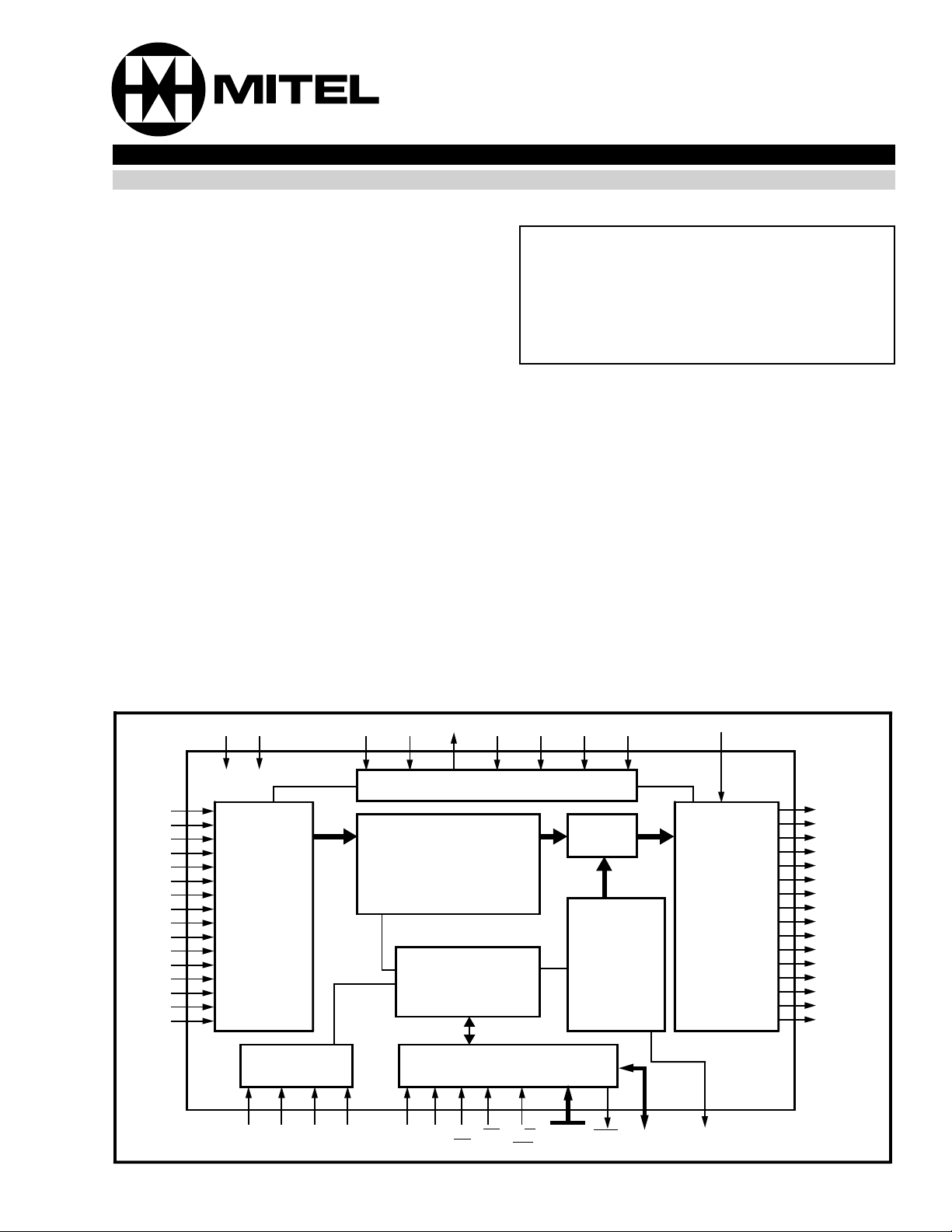
Figure 1 - Functional Block Diagram
Test Port
Interna l
Registers
Microprocessor Interface
RD
CS R/W
WR
A7-A0
Output
MUX
Connectio n
Memory
D15-D8/
DTA
AD7-AD0
ODE
Parallel
to
Serial
Converter
CSTo
STo0
STo1
STo2
STo3
STo4
STo5
STo6
STo7
STo8
STo9
STo10
STo11
STo12
STo13
STo14
STo15
2-179
Page 2
MT90820 CMOS Advance Information
ODE
STo0
STo1
STo2
STo3
STo4
STo5
STo6
STo7
VSS
STi0
STi1
STi2
STi3
STi4
STi5
STi6
STi7
STi8
STi9
STi10
STi11
STi12
STi13
STi14
STi15
FRM
FE/HCLK
VSS
CLK
VDD
VDD
STo8
STo9
ST o10
STo11
ST012
ST o13
ST o14
ST015
VSS
8
6
4
12
10
14
16
18
20
22
24
26
28
30
32
34
36
38
2
84
84 PIN PLCC
40
44
42
82
80
46
48
VSS
CSTo
74
78
76
DTA
D15
72
D14
D13
70
D12
D1 1
68
D10
D9
66
D8
64
VSS
VDD
62
AD7
AD6
60
AD5
AD4
58
AD3
AD2
56
AD1
AD0
54
50
52
VSS
STi0
STi1
STi2
STi3
STi4
STi5
STi6
STi7
STi8
STi9
STi10
STi1 1
STi12
STi13
STi14
STi15
FRM
FE/HCLK
VSS
CLK
82
84
86
88
90
92
94
96
98
100
NC
NC
NC
NC
TMS
VSS
TDI
ST015
TDO
STo14
TCK
TEST
TRSTB
RESETB
STo10
ST o11
ST012
STo13
100 PIN PQFP
\RW
R/W
ST o1
CS
ST o0
IM
AS/ALE
ODE
VSS
CSTo
NC
NC
NC
NC
525456586062646668707274767880
50
DTA
A7
A6
A5
A4
A3
A2
A1
A0
HMVIP
ST o6
ST o7
VSS
VDD
ST o8
ST o9
DS/RD
ST o2
ST o3
ST o4
ST o5
D15
48
D14
D13
46
D12
D11
44
D10
D9
42
D8
VSS
40
VDD
AD7
38
AD6
AD5
36
AD4
AD3
34
AD2
AD1
32
AD0
22 24 26 28 30
2018161412108642
VSS
2-180
NC
NC
NC
NC
A1
TDI
TCK
TDO
TMS
VDD
TRSTB
A0
TEST
HMVIP
RESETB
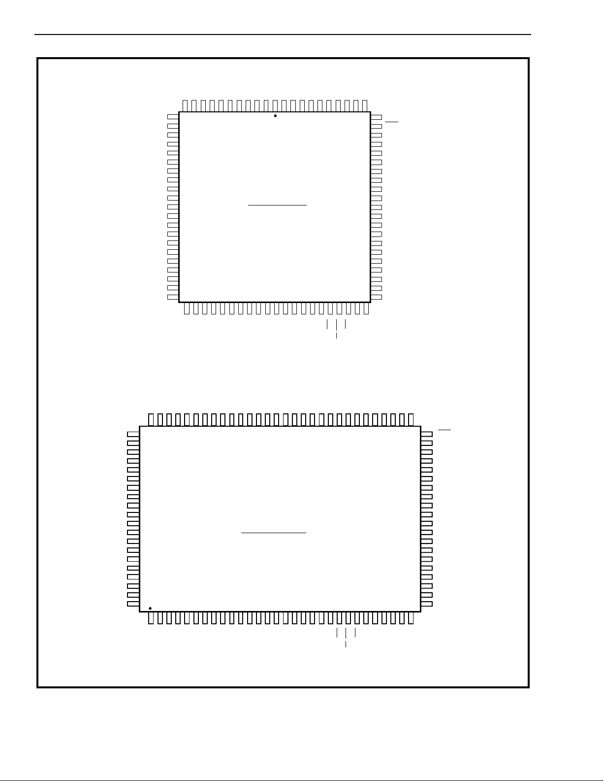
Figure 2 - Pin Connections
A2
A3
A4
A5
A6
A7
DS/RD
\RW
R/W
CS
AS/ALE
IM
NCNCNC
NC
Page 3

Advance Information CMOS MT90820
Pin Description
Pin #
84 100
Name Description
1, 11,
30, 54
64, 75
31,
41,
56,
V
SS
Ground.
66,
76, 99
2, 32,635, 40,
V
DD
+5 Volt Power Sup ply.
67
3 - 10 68-75 STo8 - 15 Data Strea m Output 8 to 15: Serial data Ou tput stream . These stream may
have data rates of 2.048, 4.096 or 8.192 M b/s.
12 - 2781-96 STi0 - 15 Data Stream Input 0 to 15: Serial data input stream. These stream may have
data rates of 2.048, 4.096 or 8.192 .
28 97 FRM Frame Pulse (input): This input accepts and automatically identifies frame
synchronization signals formatted according to ST-BUS and GCI interface
specificatio ns, when HM VIP pin =0.
When HMVIP pin =1, FRM input accepts a negative frame pulse which confo rms
to HMVIP form a ts.
29 98 FE/HCLK Frame Measurement input, when HMVIP pin = 0.
4.096MHz Clock in put, when HMVIP pin = 1.
31 100 CLK Clock (input): Serial clock for shifting data in/out on the serial stream.
33 6 TMS When 1, enable test mod e for production test ing.
34 7 TDI Test Data Input.
35 8 TDO Test Data Output.
36 9 TCK Test Clock input.
37 10 TRSTB Test Reset Input: When 0, resets the test circuit.
38 11 IC Internal Connection: keep at 0 for normal operation.
39 12 RESETB Device Reset Input: When 0, resets the device.
40 13 HMVIP HMVIP mode input. When 1, enables HMVI P interf a ce.
When 0, the device operates in ST-BUS/GCI mode.
41 - 4814-21 A0 - A7 Address 0 - 7(Input): When non-multiplexed CPU bus is selected, t hese lines
provide the A0 - A7 address lines to internal memories.
49 22 DS/RD Data Strobe/Read (input): When non-mul tiplexed CP U bus or Motorola
multiplexed bus are selected, this input is DS. This active high input works in
conjunction with CSB to enable read and write operation .
For Intel multiplexed bus, this input is RDB. This active low input sets the data bus
lines (AD0-AD7, D8-D15) as outputs.
50 23 R/W\WR Read/Write \ Write (Input): In case of non-multiplexed and Motorola m ultiplexed
buses, this input is Read/Write. This input controls the dire ction of the data bus
lines (AD0 - AD7, D8-D15) during a microprocessor access.
51 24 CS Chip Select (Input ): Active low input enabling a microprocessor access of the
device.
2-181
Page 4

MT90820 CMOS Advance Information
Pin Description
Pin #
84 100
52 25 AS/ALE Address Strobe or Latch Enable : This input is only used if multiplexe d bus is
53 26 IM CPU Interface Mode (input): If High, this input selects the mult iplexed
55 - 6232-39 AD0 - 7 Add ress/ Data Bus (Bid irectio nal ): These are bi-directional dat a pins on the
65 - 7242-49 D8 - 15 Data Bus (Bidirectional): These are additional bi-directional data pins on the
73 50 DTA Data Acknowl edg ement (Op en Drai n Output): This acti ve lo w output indicates
74 55 CSTo Control Output (output).
Name Description
selected.
microprocessor bus interface. If this input is not connected or grounded, the
device resumes non-mult iplexed bus interface.
microprocessor interface. In the multiplexed bus mode, these pin s also provide
the input address to the internal registers and memori e s.
microprocessor interface.
that a data bus transfer is complete. A 10 kohm pull-up resistor is required at this
output.
76 57 ODE Output Device Enable (input): This is the out put enable cont rol for the STo0 to
STo15 serial output s. When this input is high, the STo 0-15 outpu t drivers function
normally. If this input is low, Sto0-15 are in high impedance. Note: Even when
ODE is high, each channel may still be put into high impedance state by using per
channel control bit in the connecti on mem or y.
77 - 8458-65 STo0 - 7 Data Stream Output 0 to 7: Serial data Output stream. These streams may have
data rates of 2.048, 4.096 or 8.192 Mb/ s .
- 1 - 4,
27 -
30,
51 -
54
77 -
80
NC Unused pins.
2-182
Page 5

Advance Information CMOS MT90820
Device Over view
The LDX is capable of switching 2,048 × 2,048
channels. The device is designed to switch 64 or N x
64 kbit/s data. It can provide frame integrity for data
applications and minimum throughput switching
delay for voice application on a per channel basis.
The serial input streams of LDX can operate at
2.048, 4.096 and 8.192 Mbit/s and are arranged in
125µs wide frames which contains 32, 64 and 128
channels, respectively. The LDX automatically
identifies the polarity of the input frame
synchronization signal and configures the serial
ports to be compatible to either ST-BUS and GCI
formats. The input and output streams accept
identical data rates only.
By using Mitel message mode capability, the
microprocessor can access input and output timeslots on a per channel basis to control external
circuits or other ST-BUS devices. Two different
microprocessor bus interface can be selected
through an input mode pin (IM): Non-multiplexed or
Multiplexed. These interfaces provide compatibility
with Intel/National multiplexed and Motorola
Multiplexed/Non-multiplexed buses.
The frame offset calibration allows users to measure
the frame offset delay using an frame evaluation pin
(FE). The input stream offset delay can be
individually programmed using internal registers.
Locations in the connect memory are associated with
particular output streams. When a channel is due to
be transmitted on an output, the data for the channel
can either be switched from an input as in
connection mode or it can be from the connect
memory as in message mode. Data destined for a
particular channel on the serial output stream is read
from the data memory or connect mem o ry d u rin g th e
previous channel time-slot. This allows enough time
for memory access and parallel to serial conversion.
Connection and Mess age Mo des
In Connection mode, the addresses of the inputs for
all output channels are stored in the connect
memory. Once the source addresses are
programmed by the CPU, the contents of the data
memory at the selected address are transferred to
the parallel-to-serial inverters. By having the output
channel specifying the source channel through the
connect memory, the user can route the same input
channel to serval output channels, allowing
broadcast fa c i lity w ith i n the switch.
In message mode, the CPU writes data to the
connect memory locations corresponding to the
output link and channel number. The lower half (8LSBs) of the connect memory content is transferred
directly to the parallel-to-serial converter one
channel before it is to be output. The data is
transmitted on to the output every frame until it is
changed by the CPU with a new data.
Functional Description
A functional Block Diagram of the LDX device is
shown in Figure 1. Depending upon the application,
the LDX device receives TDM serial data at diff erent
rates.
Data and Connect Memory
For all data rates, the received serial data is
converted to parallel format by the serial to parallel
converters and stored sequentially in a Data
Memory. Depending upon the selected operation, the
data memory may have up to 2,048 bytes in use. The
sequential addressing of the data memory is
performed by an internal counter which is reset by
the input 8 kHz frame pulse (FRM) marking the
frame boundaries of the incoming serial data
streams.
Data to be output on the serial streams may come
from two sources: Data Memory or Connect Memory.
The five most significant bits in the connect memory
determine individual output channel to be in
message or connection mode, select output
throughput delay type, enable/disable output drivers
and enable/disable the loopback mode. In addition,
one of these bits allows the user to control the CSTo
output.
If an output channel is set to high-impedance, the
TDM serial stream output will be in high impedance
during that channel time. In addition to the perchannel control, all channels on the TDM outputs
can be placed in high impedance by either pulling
the ODE input pin low or programming a particular
bit in the c o ntrol r e giste r.
The connect memory data is received via the
microprocessor interface through the data I/O bus.
The addressing of the LDX internal registers, data
and connect memories is performed through address
input pins and the Memory Select bit in the control
register.
2-183
Page 6

MT90820 CMOS Advance Information
Serial Data Interface
The master clock (CLK) can be either at 4.096, 8.192
or 16.384 MHz allowing serial data link operation at
2.048, 4.096 and 8.192 Mb/s respectively. The
master clock frequency is always twice the data rate.
The input and output streams accept identical data
rate.
The input 8 kHz frame pulse can be in either ST-BUS
or GCI format. The LDX automatically detects the
presence of an input frame pulse and identifies the
type of serial interface. In ST-Bus format, every
second falling edge of the master clock marks a bit
boundary and the input data is clocked by the rising
edge, three quarters of the way into the bit cell. In
GCI format, every second rising edge of the master
clock marks the bit boundary while data sampling is
performed on the falling edge, at three quarters of
the bit cell boundary.
Switching Configuration
Switching configurations are determined basically by
the data rates selected at the serial inputs and
outputs. To specify the switching configuration
required, the Interface Mode Selection (IMS) register
has to be initialized on system power-up. The
switching configuration is selected by two DR bits in
the IMS re g iste r.
Serial Links with Data Rates at 2.048 Mb/s
When the 2.048Mb/s data rate is selected for input
and output streams, the device is configured with 16input/16-output data streams with 32 64Kbit/s
channels each. The modes allows 512 x 512 channel
Switch Matrix configuration. The interface clock is
4.096 M Hz.
Serial Links with Data Rates at 4.096 Mb/s
When the 4.096 Mb/s data rate is selected for input
and output streams, the device is configured with 16-
input/16-output data streams with 64 64Kbit/s
channels each. The modes allows 1,024 x 1,024
channel Switch Matrix configuration. The interface
clock is 8.192MHz.
Serial Links with Data Rates at 8.192 Mb/s
When the 8.192Mb/s data rate is selected for input
and output streams, the device is configured wit h 16input/16-output data streams with 128 64Kbit/s
channels each. The modes allows 2,048 x 2,048
channel Switch Matrix configuration. The interface
clock is at 16.384 MHz.
Table 1 summarizes the switching configurations.
Input Frame Offset Selection
The LDX provides a feature called Input Frame
Offset allowing users to compensate for the varying
delays on the incoming serial inputs while building
large switch matrices. Usually, different delays occur
on the digital backplanes causing the data and frame
pulse signal to be skewed at the input of the switch
device. This may result in the system frame pulse to
be active at the FRM input before the first bit of the
frame is received at the serial input.
The LDX allows users to compensate the input delay
offset by programming the Frame Input Offset (FOS)
registers. Each input stream can have its own delay
offset value. Possible adjustment is up to 4 master
clock periods forward with resolution of 1/2 clock
period.
Frame Alignment Evaluation
To manage the problem of diff erent data input delays
(with respect to the frame pulse), the LDX provides
the FE input for the frame alignment evaluation. The
evaluation starts when the SFE bit in the IMS
register is changed from low to high. Two frames
later, the CFE bit of the frame alignment register
(FAR) changes from low to high to signal the CPU
Serial
Interface
Data Rate
2 Mb/s 4.096 16 x 16 512 x 512 Non-Blocking STi0-15/STo0-15
4 Mb/s 8.192 16 x 16 1,024 x 1,024 Non-Blocking STi0-15/STo0-15
8 Mb/s 16.384 16 x 16 2,048 x 2,048 Non-Blocking STi0-15/STo0-15
Master
Clock
Required
(MHz)
Number of
Input x
Output
Streams
Matrix Channel
Capacity
Switch Matrix type
Input/Output Stream
Table 1: Switching Configuration
2-184
used
Page 7

Advance Information CMOS MT90820
that a valid offset measurement is ready to be read
from the FAR registe r.
This feature is not available when the HMVIP
interface is enabled, i.e. when HMVIP pin is tied to
.
V
DD
Memory Block Programming
The LDX device provides the capability of block
programming the connect memory block. By using
this feature, the five MSBs of the connect memory
belonging to each output channel can be
automatically programmed with a fixed pattern
defined by the IMS register. This feature reduces the
system initialization time.
To enable the block programming mode, user have
to set the Memory Block Program (MBP) bit of the
control register to HIGH and program the IMS
register with the Block Programming Enable (BPE)
bit = 1, and the desired pattern. The block
programmin g ta ke s tw o fra mes to comp lete.
Delay Through the LDX
connected HIGH, the internal parallel microport
provides compatibility to MOTEL interface allowing
direct connection to Intel, National and Motorola
CPUs.
The MOTEL circuit (MOtorola and inTEL compatible
bus) automatically identifies the types of CPU Bus
connected to the LDX. This circuit uses the level of
the DS/RD
to identify the appropriate bus timing connected to
the LDX. If DS/RD
ALE then Motorola bus timing is selected. If DS/RD
is HIGH at the rising edge of AS/ALE, then the Intel
bus timing is selected.
The LDX microport provides the access to the
internal registers, connect and data memories. All
locations can be read or written except for the data
memory which can be read only.
input pin at the rising edge of the AS/ALE
is low at the rising edge of AS/
Internal Register and Addres s M emory
To access internal registers, users have to connect
the A7 pin to LOW. To access to data and connect
memories positions, users have to connect the A7
pin H I GH.
The switching of information from the input serial
streams to the output serial streams results in a
delay. Depending on the type of information to be
switched, the LDX can be programmed to perform
time-slot interchange functions with different
throughput delay capabilities on the per-channel
basis. For voice application, variable throughput
delay can be selected ensuring minimum delay
between input and output data. In wideband data
applications, constant throughput delay can be
selected maintaining the frame integrity of the
information through the switch.
The delay through the LDX varies according to the
type of throughput delay selected in the connect
memory.
Microprocessor Port
The LDX provides an microprocessor interface with
non-multiplexed and multiplexed bus structures. The
LDX microport is compatible to Motorola multiplexed/
non-multiplexed and Intel multiplexed buses. The
multiplexed bus structure is selected by the CPU
interface Mode (IM) pin.
Table 2 summarizes the internal register and address
memory mapping.
Initializa tion of the L DX
On initialization or power up, the contents of the
connect memory can be in any states. This is a
potentially hazardous condition when multiple LDXs
outputs ar e tied together to fo rm matrices, as thes e
output may conflict each other. The ODE pin should
be held low on power up to keep all outputs in the
high impedance condition.
When the IM pin is not connected (left open) or
grounded, the LDX parallel port assumes the default
Motorola non-multiplexed bus mode. If IM pin is
2-185
Page 8

MT90820 CMOS Advance Information
A7 A6 A5 A4 A3 A2 A1 A0 Location
0 0 0 0 0 0 0 0 Control Register, CAR.
0 0 0 0 0 0 0 1 Interface Mode Selection register, IMS
0 0 0 0 0 0 1 0 Frame Alignment register, FAR
0 0 0 0 0 0 1 1 Frame Input Offset register 0, FOS0
0 0 0 0 0 1 0 0 Frame Input Offset register 1, FOS1
0 0 0 0 0 1 0 1 Frame Input Offset register 2, FOS2
0 0 0 0 0 1 1 0 Frame Input Offset register 3, FOS3
Ch 0*
1
1
1
1
1
1
1
1
1
1
0
0
0
0
0
0
0
0
0
0
0
0
0
0
0
1
1
1
1
1
0
0
.
1
1
0
0
.
1
1
0
0
.
1
1
0
0
.
1
1
0
0
.
1
1
0
0
.
1
1
0
0
.
1
1
0
0
.
1
1
0
Ch 1*
1
.
.
Ch 30*
0
Ch 31*
1
Ch 32**
0
Ch 33**
1
.
.
Ch 62**
0
Ch 63**
1
Ch 64***
1
1
1
1
1
Note 1: The bit A7 must be retained HIGH for accesses to Data and Connection Memory positions.
Note*: Channel 0 to 31 are used in 2Meg mode.
Note**: Channel 0 to 63 are used in 4Meg mode.
Note***: Channel 0 to 127 are used in 8Meg mode.
1
1
1
1
1
The bit A7 must be retained LOW for accesses to Registers.
0
0
.
1
1
0
0
.
1
1
0
0
.
1
1
0
0
.
1
1
0
0
.
1
1
0
1
.
0
1
Ch 65***
.
Ch 126***
Ch 127***
Table 2 - Internal Register and Address Mem or y Mapping
2-186
Page 9

Advance Information CMOS MT90820
Absolute Maximum Ratings*
Parameter Symbol Min Max Units
Supply Voltage
1
Voltage on any pin I/O (other than supply pins)
2
Current at digital outputs
3
Package power dissipation
4
Storage temperature
5
* Exceeding these figures may cause permanent damage. Functional operation under these conditions is not guaranteed.
VDD 6.0 V
VV
I
O
P
D
T
ST
- 0.3 VDD + 0.3 V
SS
40
2
- 65
150
mA
°C
W
Recommended Operating Conditions - Vol ta ges are with respect to ground (V
) unless otherwise stated.
SS
Characteristics Sym Min Typ* Max Units Test Conditions
1 Operating Temperature T
2 Positive Supply V
3 Input Voltage V
OP
DD
I
4.75 5.0 5.25 °C
4.75 5.0 5.25 V
0V
DD
V
* Typical figures are at 25°C and are for design aid only; not guaranteed and not subject to production testing.
DC Electrical Characteristics - Voltages are with respect to ground (V
) unless otherwise stated.
SS
Characteris tics S ym Min Typ Max Units Test Conditions
1
2 Input Voltage High V
3 Input Voltage Low V
4 Input Leakage (input pins)
5 Input Pin Capacitance C
6
7 Output Voltage Low V
8 Output High Current I
9 Output Low Current I
10 High Impedance Leakage I
Supply Current I
I
N
P
U
T
S
Input Leakage (I/O pins)
Output Voltage High V
O
U
T
P
U
T
S
DD
I
IL
OH
OL
OH
OL
OZ
50 mA Output unloaded
2.0 V
IH
IL
34
I
8pF
0.8 V
5
100
µAµAV
2.4 V IOH = 10mA
0.4 V IOL = 5mA
10 mA Sourcing. VOH=2.4V
5 mA Sinking. VOL=0.4V
5 µA
between V
I
SS
and V
DD
11 Output Pin Capacitance C
O
8pF
2-187
Page 10

MT90820 CMOS Advance Information
NOTES:
2-188
 Loading...