

Page 1
CMOS
MT90810
Flexible MVIP Interface Circuit
Preliminary Information
Features
•MVIP and ST-BUS compliant
• MVIP Enha nced Switch ing wi th 384x 384
channel ca paci ty (25 6 MVI P chan nels; 128
local channels)
• On-chip PLL for MVIP master/slave operation
• Local outpu t clock s of 2.04 8,4.09 6,8.1 92MH z
with programm abl e pola rity
• Local serial interface is programmable to
2.048, 4.09 6, or 8 .192M b/s wi th asso ciate d
clock outputs
• Additiona l con trol out put s tream
• Per-channel mess age mode
• Two independently progra mm able gro ups of up
to 12 framing signals each
• Motorola non -mul tiplexe d or Intel mu ltiple xed /
non-multip lexed mi crop roces sor interfa ce
•
Applications
• Medium si ze digi tal sw itch matr ices
• MVIP interface functions
• Serial bus co ntrol an d mon itoring
• Centralized voice processing systems
• Voice/Data multip lexer
ISSUE 2 October 1994
Ordering Information
MT90810AK 100 Pin PQFP
0 °C to +70 °C
Descript io n
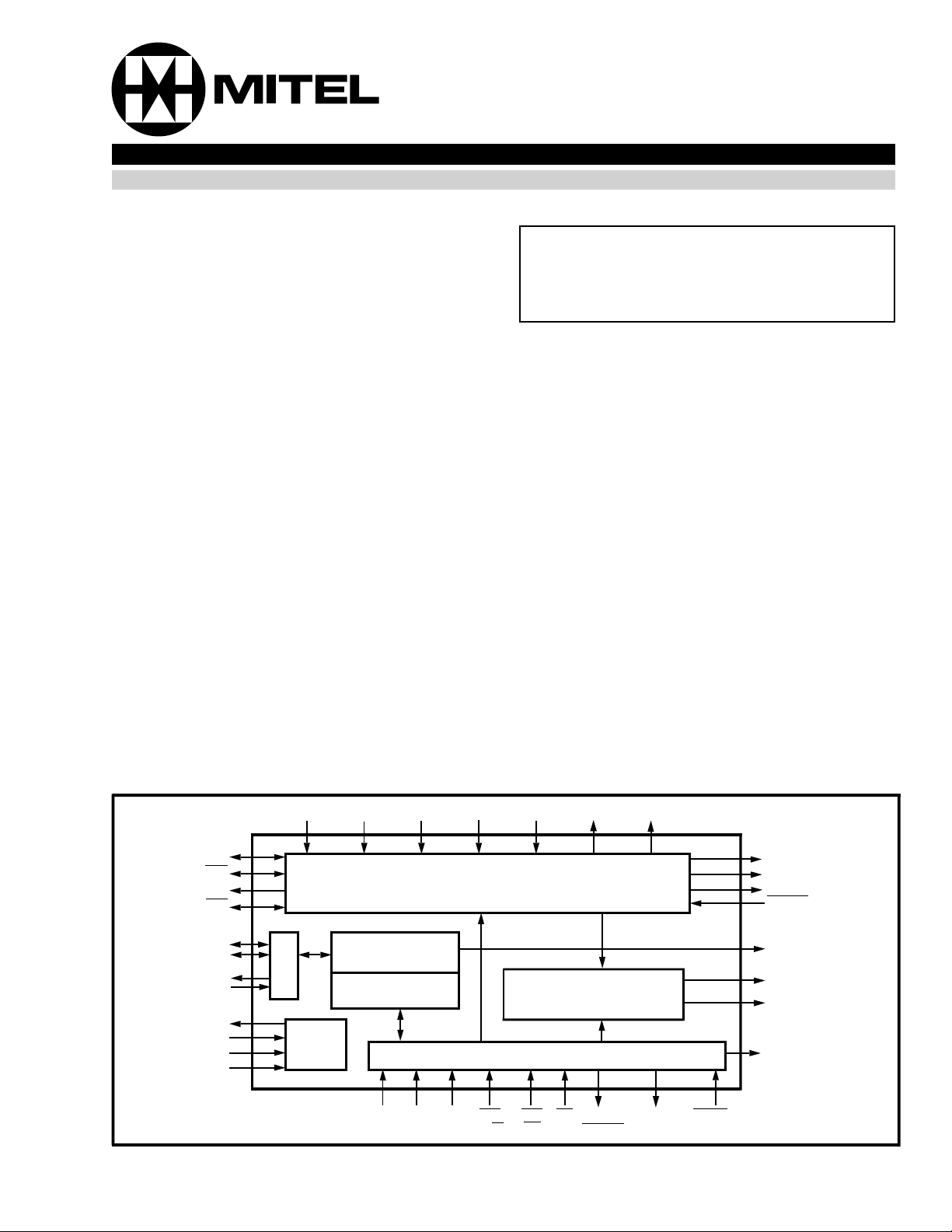
Mitel’s MT90810 is a Flexible MVIP Interface Circuit
(FMIC). The MVIP (Multi-Vendor Integration
Protocol) compliant device provides a complete
MVIP compliant interface between the MVIP Bus
a wide variety of processors, telephony interfaces
and other circuits. A built-in digital time-slot switch
provides MVIP enhanced switching between the full
MVIP Bus and any combination of up to 128 full
duplex local channels of 64kbps each. An 8 bit
microprocessor port allows real-time control of
switching and programming of device configuration.
On-board clock circuitry, including both analog and
digital phase-locked loops, supports all MVIP clock
modes. The local interface supports PCM rates of
2.048, 4.096 and 8.192Mb/s, as well as parallel DMA
through the microprocessor port.
and
SEC8K
C4b
C2o
F0b
DSo[0:7]
DSi[0:7]
LDO[0:3]
LDI[0:3]
TCK
TMS
TDI
TDO
EX_8KA
S-P/
P-S
JTAG
EX_8KB
Enhanced Switch
Data Memory
Connection Memory
AD[0:7] RDY/
X2 X1/CLKIN PLL_LO PLL_LI FRAME
Timing and Clock Control
(Oscillator and Ana lo g & Digital PLLs)
Programmable
Microprocessor Interface
WR/
ALEA[0:1] DREQ[0:1] DACK[0:1]
R/W
CSRD/
DS
Figure 1 - Functional Block Diagram
Framing Sig na ls
DTACK
CLK2
CLK4
CLK8
RESET
CSTo
FGA[0:11]
FGB[0:11]
ERR
2-145
Page 2
MT90810 Preliminary Information
LDO0
VSS
DSi7
DSo7
FGB9
DSi6
DSo6
DSi5
DSo5
DSi4
DSo4
FGA9
DSi3
DSo3
VSS
VDD
DSi2
DSo2
FGB8
DSi1
DSo1
DSi0
DSo0
FGA8
C4b
F0b
C2o
SEC8K
VSS
FGB7
525456586062646668707274767880
FGA10
LDO1
LDO2
FGB10
LDO3
VDD
LDI0
LDI1
LDI2
LDI3
EX8_KA
EX8_KB
VSS
FRAME
CLK8
FGA11
CLK4
CLK2
FGB11
FGA0
82
84
86
88
90
92
94
96
98
100
100 PIN PQFP
22 24 26 28 30
2018161412108642
50
DREQ1
DREQ0
48
DACK1
DACK0
46
FGA7
AD7
44
AD6
AD5
42
AD4
VSS
40
VDD
FGB6
38
AD3
AD2
36
AD1
AD0
34
A1
FGA6
32
A0
ERR
TDI
TCK
TDO
CSTo
FGA1
FGA2
FGA3
FGA4
FGB0
FGB1
FGB2
FGB3
TMS
FGB4
X2
VSS
VDD
FGA5
RESET
X1/CLKIN
PLL_LI
PLL_LO
VCO_VSS
CS
ALE
FGB5
RD/[DS]
WR/[R/W]
VCO_VDD
RDY/[DTACK]
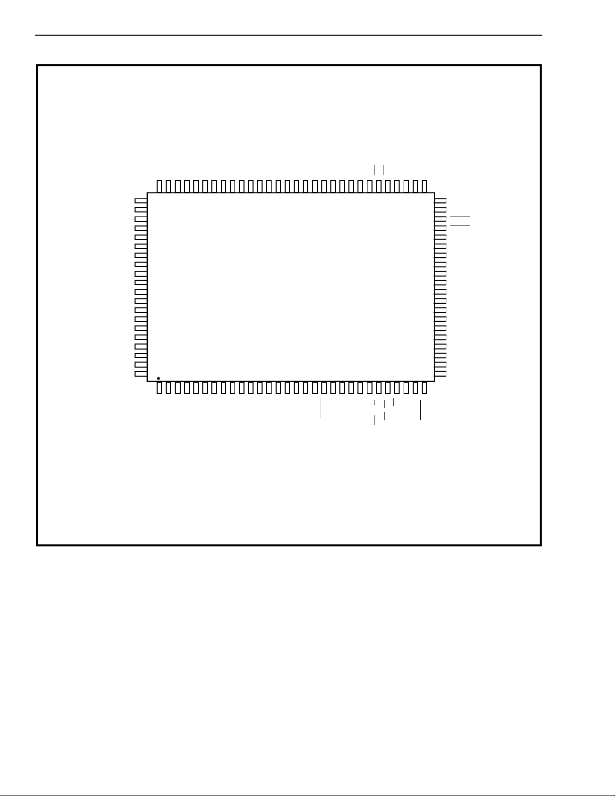
Figure 2 - Pin Connections
2-146
Page 3

Preliminary Information MT90810
Pin Description
Pin # Name Descri ptio n
58, 60, 63, 67, 70,
72, 74, 77
59, 61, 64, 68, 71,
73, 75, 78
80, 82, 83, 85 LDO[0:3] Local Output Seria l Str eam s (Output ). Serial data streams
87, 88, 89, 90 LDI[0:3] Local Input Seri al Streams (TTL Input). Serial data stream s
4CSToControl ST-BUS Output (Output). This is a 1.024Mb/s outpu t. The
55 F0b
56 C4b
54 C2o MVIP C2 signal (Outp ut). ST-BUS 2.048MHz clock. This pin is
53 SEC8K MVIP SEC8K signal (CMOS Input/Output). A secondary 8kHz signal
91 EX_8KA External 8k Hz input A (TTL Input).
92 EX_8KB External 8k Hz input B (TTL Input).
DSo[0:7] MVIP DSo Stre am s (Bid irectional CMO S ). 2.048M b/s serial dat a
streams conforming to ST-BUS serial data stream specifications.
DSi[0:7] MVIP DSi Str eams (Bidirectional CMOS ). 2.048M b/s serial dat a
streams conforming to ST-BUS serial data stream specifications.
programmabl e to 2.048, 4.096 or 8.192 Mb/ s data rat es.
programmabl e to 2.048, 4.096 or 8.192 Mb/s data rates.
state of each bit in this stream is determined by the CSTo bit in
connection memory high.
MVIP F0 signa l (CMOS Input/Output). ST-BUS 8kHz framing signal
MVIP C4 signal (CMOS Input/Output). ST-BUS 4.0 96M Hz clock
automatically set to high im pedance when it is not driven.
used either as an input source to the on-chip digital PLL or as an
output to t he M V IP b us .
94 FRAME Local Frame Output Signal (Output). This 8kHz framing signal has a
duty cycle and period equal to the MVIP F0
95 CLK8 8MHz Local Outpu t Clock (Output ). This is a 8MHz clock.
97 CLK4 4MHz Local Outpu t Clock (Output ). Thi s 4MHz cloc k has a duty
cycle and period equal to the MVIP C4
98 CLK2 2MHz Local Outpu t Clock (Output ). Thi s 2MHz cloc k has a duty
cycle and period equal to the MVIP C2 signal.
100, 1, 2, 3, 5, 20,
33, 46, 57, 69, 81,
96
6, 7, 8, 9, 14, 28,
39, 51, 62, 76, 84,
99
19 RESET
35, 36, 37, 38, 42,
43, 44, 45
FGA[0:11] Frame Gro up A framing sign al s (Output). Programmable framing
signals. The frame gro up outp uts are determ ine d by mode bit s in the
frame register to be either programme d output s, out put drive enables
for DSo, or output framing pul se s for use with local serial dat a
streams.
FGB[0:11] Frame Gro up B framing sign al s (Output). Programmable framing
signals. The frame gro up outp uts are determ ine d by mode bit s in the
frame register to be either programme d output s, out put drive enables
for DSi, or output framing pulses for use with local serial data streams.
Chip Reset (Schmitt Input). This active low reset clears all internal
registers, connection memory and data memory
AD[0:7] Microprocessor Address/Data Bus (Bidirecti onal TT L).
Microprocessor access to internal registers, connection and data
memories.
In non-multiplexed mode: data bu s.
In multiplexed mode: multiplexed address and data bus.
signal.
signal.
2-147
Page 4

MT90810 Preliminary Information
Pin Description
Pin # Name Des cri ptio n
32, 34 A[0:1] Microprocessor Address (TTL Input).
In non-multiplexed mode: address to FMIC internal registe rs
In multiplexed mode: unuse d (leave unconnecte d ).
29 ALE Microprocessor Address Latch Enable (TTL Inp ut). Selects the
microprocessor mode.
In Intel multiplexed mode, the falling edge of this signal is used to
sample the address.
27 CS
26 RD
25 WR
30 RDY [DTACK
31 ERR Error Status (Output). This pin is asserted high if either a clock error
/ [DS] Read/Data Strobe (TTL Input).
/ [R/W] Write\ Read/Write Strob e (TTL Input).
Microproc esso r Bus Chi p Select (TT L Input). Th is active low input
enables microprocessor access to connection and data memor y and
internal registers.
In Intel mode (RD
as output.
In Motorola mode (DS
enable read and write operati on.
In Intel mode (WR
as inputs.
In Motorola mode (R/W
bus D[0:7] during a microprocessor access.
] Ready/Data Ackno wl ed ge (Open Drain Outpu t).
In Intel mode (RDY), this output acts as IOCHRDY. A 10K pull up is
required.
In Motorola mode (DTACK
successful data bus transfer. A 10K pull up is required.
(loss of C4b
), this active low input configures the data bus lines
), this active low input operates with CS to
), this active low input configure s the data bus lines
), this input controls the direct ion of the data
), this active low output indicates a
clock), DMA overrun condition or PLL unlock occurs.
49, 50 DREQ[0:1] DMA Request (Output). When DM A operation s on the device are
enabled, thi s pin requests t ransf e rs for DMA read s/writ es f rom /to the
device.
47, 48 DACK
10 TCK JT AG Input Clock (TTL Input). Maximum recommended clock rate is
11 TDI JT AG Seri al Inp ut Data (TTL Input). If not used, this pin should be left
2-148
[0:1] DMA Acknowledge (TTL Input). When DMA operations on the device
are enabled, this pin receives acknowledgement for DMA reads/writes
from/to the device.
16 MHz. If not used, this pin should be left unconnecte d.
unconnected.
Page 5

Preliminary Information MT90810
Pin Description
Pin # Name Descri ptio n
12 TDO JT AG Serial Output Data (Output). If not used, this pin should be left
unconnected.
13 TMS JTAG Mode Control Input (TTL Input). If not used, this pin should be
left unconnected.
17 X1/CLKIN Clock Input Pin/ Crystal Oscillator Pin1.
18 X2 Crystal Oscillator Pin 2 (Input). If X1 is clock input, this pin should be
left unconnected.
22 PLL_LO PLL Loop Filter Output. (Output 6mA drive).
23 PLL_LI P L L L oo p Filte r Inp u t. (1 µA Low level/High level Input current).
21 VCO_VSS Ground for On-chip VCO.
24 VCO_VDD +5 Volt Power Supp ly for On-chi p VC O.
15, 40, 65, 86 VDD[0:3] +5 Volt Power Supply.
16, 41, 52, 66,
79, 93
VSS[0:5] Ground .
Device Over view
Mitel’s MT90810 is a MVIP compliant device. It
provides a complete, cost effective, MVIP compliant
interface between the MVIP Bus
of processors, telephony interfaces and other
circuits. The FMIC supports 384 full duplex, time
division multiplexed (TDM), channels. These
channels are divided into 256 full duplex MVIP
channels and 128 full duplex local channels. The
sample rate for each channel is 8kHz and the width
of each channel is 8 bits for a total data rate of
64kbits/s per channel.
The FMIC’s internal clock circuitry includes both an
analog and a digital PLL and supports all MVIP clock
modes. The device can be configured as a timing
master whereby an external 16.384MHz crystal or
4.096, 8.192 or 16.384MHz external clock source is
used to generate MVIP clock signals. The device can
also operate as a slave to the MVIP bus,
synchronizing its master clock to the MVIP 4MHz
bus clo c k .
The device’s local serial interface supports PCM
rates of 2.048, 4.096 and 8.192Mb/s, per channel
message mode, an additio nal c ontrol s tre a m, as wel l
as parallel DMA through the microprocessor port.
Furthermore, the FMIC’s programmable group of
output framing signals and local output clocks may
be used to provide the appropriate frame and clock
pulses to drive other local serial buses such as GCI.
A microprocessor interface permits reading and
writing of the data memory, connection memory and
all internal control registers. The Connection and
and a wide variety
Data memory can be read and updated while the
MVIP bus is active, that is, connections can be made
without interrupting bus activities.
Functional Description
Switching
The FMIC provides for switching of data from any
input channel to any output channel. This is
accomplished by buffering a single sample of each
channel in an on-chip 384 byte static RAM. Samples
are written into this data RAM in a fixed order and
read out in an order determined by the programming
of the conn e ct i on m e mory. An input shift re gis te r a n d
holding latch for each input stream make up the
serial to parallel conversion blocks on the input of
the FMIC and an output holding register an shift
register make up the parallel to serial conversion
blocks on the output of the FMIC.
Data Memory
Data memory is a 384 byte static RAM block which
provides one sample of buffering for each of the 384
channels. An input shift register and holding latch for
each input stream make up the serial to parallel
conversion blocks on the input. Each input channel is
mapped to a unique location in the RAM, as shown
Table 18 - “Data Memory Mapping”.
Data memory can be read and written by the
microprocessor (See “Software Control” for further
details). Note that writing to data memory may be
futile since the contents will be overwritten by
incoming data on the serial input streams.
2-149
Page 6
MT90810 Preliminary Information
DC=0 for stream 0 channel 1
O/P
0123 3029 31
Connection Memory
Connection memory is comprised of a static RAM
block 384 locations by 12 bits. Each location in
connection memory corresponds to one of the 384
output channels. The mapping of memory location to
output channel is the same as the mapping of input
channel to data memory location and is shown in
Table 19 - “Connection Memory Mapping”.
The lower 8 bits of connection memory form
connection memory low byte as shown in Figure 10 “Connection Memory Low Byte”. The bits are defined
in Table 20, “Connection Memory Low Bits”.
The upper 4 bits of connection memory form
connection memory high (refer to Figure 11 “Connection memory high byte” ). Connection
memory low byte, together with the least significant
bit of connection memory high form an address to
point to in data memory. The location pointed to in
data memory provides the data for a given output
channel. The remaining three bits in connection
memory high are control bits. These bits perform
slightly different functions for MVIP and local
channels. The control bits in connection memory
high for MVIP streams enable/disable output drivers,
specify message or connection mode for individual
output channels, and determine the direction of the
DSi/DSo channel pair (see Table 21 - “Connection
Memory High Bits for MVIP channels” for further
details). The control bits in connection memory high
for local streams enable/disable DMA transfer,
specify message or connection mode for individual
output channels, and control CSTo timing (see Table
22 - “Connection Memory High Bits for Local
channels” fo r fu rth e r de ta il s) .
Connection memory can be read and written by the
microprocessor (see “Software Control” for further
details). When writing to connection memory, it is
necessar y to first w rite the low b its and th en t he h ig h
bits. The low bits are held in a temporary register
until the high bits are written. The comp lete write of
all 12 bits (to connection memory) is only performed
when the high bits are being written.
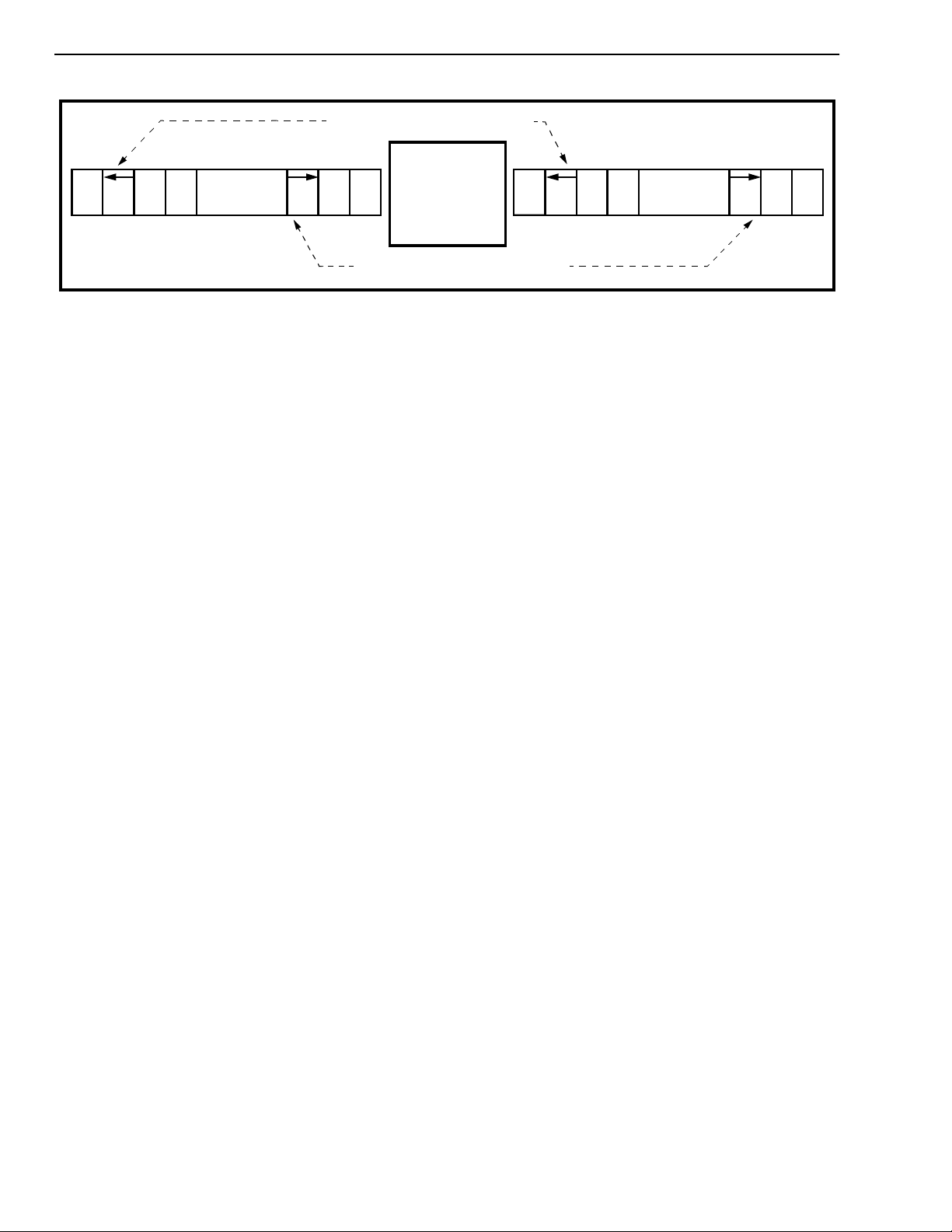
DSi0
. . . . .
I/P
DC=1 for stream 0 channel 29
Figure 3 - Per -chan nel Dir ectio n Co ntrol
I/P
FMIC
Connection and Message Modes
In connection mode, the connection memory low
byte and the least significant bit of connection
memory high form a 9 bit address to point to in data
memory. The location pointed to specifies which
source/input channel to connect to the respective
output channel and stream. The same source
channel can be routed to various output channels,
thus providing broadcast facility within the switch.
In message mode, the connection memory low byte
is sent directly out the corresponding output channel
and stream. The least significant bit of connection
memory high is not used.
Direction Control Bit
The direction control (DC) bit in connection memory
high determines the direction of the associated DSiDSo channel pair. If the DSi or DSo channel is
programmed as an input, the corresponding DSo or
DSi channel will automatically be configured as an
output. Thus, there are always 256 MVIP input and
256 MVIP output channels or 256 full duplex MVIP
channels on the MVIP bus. Figure 3 - “Per channel
direction control” illustrates the use of DC bit for
direction control on stream 0 channel 1 and channel
29. When DC bit is set, DSo channel is output from
the FMIC and DSi is input to the FMIC. When DC bit
is cleared, the channel directions are reversed.
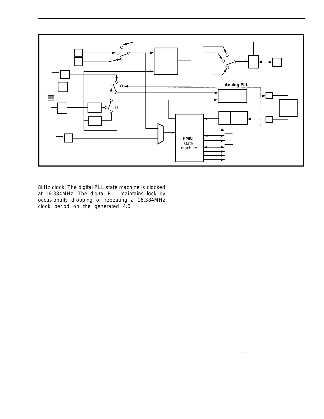
Timing and Clock Control
The FMIC clock control circuitry contains an on-chip
analog PLL (with external loop filter) which is
designed to phase lock to a 4.096MHz clock. The onchip VCO runs at eight times this rate yielding a
32MHz clock which is divided by two. The resulting
16.384MHz is used as the internal master clock of
the FMIC.
The input to the analog PLL can be selected from
among several different sources including, the MVIP
C4 clock which is used as the internal master clock
of the FM IC.
The on-chip digital PLL generates a 4.096MHz clock
which is phase locked to an externally generated
0123 3029 31
DSo0
. . . . .
O/P
2-150
Page 7
Preliminary Information MT90810
AAAA
AAAA
AAAA
AAAA
AAAA
AAAA
AAAA
AAAA
AAAA
AAAA
AAAA
SEC8K
EX_8KA
EX_8KB
C4b
X2
External
16MHz Crystal
X1
F0b
div 4
div 2
2, 6
0
0
1
1, 5
PLL_MODE
3, 7
16MHz
4
PLL_MODE
XCLK_SEL
2
External 8kHz
Digital
PLL
(sampler)
Jittery 4.096MHz
60ns peak jitter
8kHz
EX_8K A
EX_8K B
div 4
FMIC
state
machine
FRAME
4.096MHz
16MHz
0
SEL_S8K
1
2
Analog PLL
Phase
Comparator
VCO
div
by 2
@32MHz
FRAME
F0b
CLK8
C4b
CLK4
C2o
CLK2
EN_SEC8K
up/
down
SEC8K
PLL_LO
external
loop
filter
PLL_LI
Figure 4 - Clock Control Functional Block Diagram
8kHz clock. The digital PLL state machine is clocked
at 16.384MHz. The digital PLL maintains lock by
occasionally dropping or repeating a 16.384MHz
clock period on the generated 4.096MHz clock.
Consequently, the 4.096MHz clock has jitter equal to
about 60ns. If the output of the digital PLL is chosen
as the input to the analog PLL, a slow loop filter with
a time constant greater than several 8kHz frames will
smooth out the jitter.
The clock oscillator pins X1 and X2 can be used with
an external 16.384MHz crystal or pin X1 can be used
directly as a clock input with X2 left unconnected.
When X1 is used as a clock input, the frequency of
the clock can be selected to be either 16.384MHz or
8.192MHz or 4.096MHz by changing the XCLK_SEL
bits i n the CLK_CNT L reg i ster.
The overall FMIC state machine from which all timing
is derived, is clocked by the 16.384MHz output of the
analog PLL, the device’s master clock. The state
machine controls all timing in the FMIC and has a
period equal to one MVIP frame (8kHz). This state
machine can either free run or synchronize to an
8kHz source such as the MVIP F0 signal or an
external 8 kH z reference .
Refer to Figure 4 - “Clock Control Functional Block
Diagram” for further details.
The operation of the PLLs and the state machine is
controlled by the clock control register as described
in Figure 6 - “Clock Control (CLK_CNTRL) Register”
and Tables 8 to 10. The clock circuitry (PLLs and
state machine) operates in eight different modes.
They are:
FMIC as Timing Master (Mode 0)
The FMIC is configured as the timing master
(CLK_CNTRL register cleared, PLL mode 0
selected) after reset. The external 16.384MHz input
is divided by four and used as the input to the analog
PLL so the internal master clock is phase locked to
the 16.384MHz oscillator. The FMIC state machine is
free-running and does not synchronize to any
external 8kHz source.
In this mode, the XLCK_SEL bits of the clock control
register can be programmed to accommodate an
8.192MHz or 4.096MHz external clock instead of the
default 16.384MHz.
The FMIC becomes MVIP master when MVIP_MST
bit is set in the Control/Status register. This mode
can be used when the FMIC chip is to become timing
master in a system which has no digital network
connections (T1 or E1).
FMIC as MVIP Slave ( M od e 4 )
When this mode is selected, MVIP C4
clock is
selected as the input to the analog PLL. The FMIC
internal master clock is then synchronized to the
MVIP bus timing. The FMIC state machine is also
synchroniz e d to the M VI P F0
framing signal.
The MVIP_MST bit in the Control/Status register
should never be set when the device is in mode 4 as
the FMIC is entirely sl a ve to the M VIP bus t im ing .
2-151
Page 8
MT90810 Preliminary Information
0
0
2
Jitter
Attenuation
(dB)
-2
4
-4
6
-6
8
-8
10
-10
12
-12
14
-14
16
-16
0 123456
1 10 100 1K 10K 100K
-2
-4
-6
-8
-10
-12
-14
-16
Frequency, log scale (Hz)
Figure 5 - Jitter Transfer Function of the Analog PLL
FMIC as MVIP Mast e r (Mode 1,2, 3)
In modes 1 through 3, the output of the device’s
digital PLL is selected as the input to the analog PLL.
The source to the digital PLL is selected as either
SEC8K, EX_8KA or EX_8KB depending on the
particular mode (1, 2 or 3) chosen.
In these modes, the FMIC state machine is not
synchronized to the external 8kHz input selected,
that is, the state machine output 8kHz FRAME and
signals may not be phase aligned with the
F0b
external 8kHz input but will always be frequency
locked.
In modes 1, 2 and 3, the external clock X1 must be
16.384MHz. This is required for proper operation of
the digital PLL.
The FMIC becomes MVIP master when MVIP_MST
bit is set in the Control/Status register.
FMIC as MVIP Mast e r (Mode 5,6, 7)
In modes 5 through 7, the output of the device’s
digital PLL is selected as the input to the analog PLL.
The source to the digital PLL is selected as either
SEC8K, EX_8KA or EX_8KB depending on the
particular mode (5, 6 or 7) chosen.
In these modes, the FMIC state machine is
synchronized to the external 8kHz input selected,
that is, the state machine output 8kHz FRAME and
signals are phase aligned with the external 8kHz
F0b
input as well as frequency locked. Here lies the
difference between these modes (5, 6 and 7) and the
above mentioned modes (1, 2 and 3). In these
modes, the external 8kHz input signal is used to
synchronize the FMIC state machine.
Series 1
In modes 5,6 and 7, the external clock X1 must be
16.384MHz. This is required for proper operation of
the digital PLL.
The FMIC becomes MVIP master when MVIP_MST
bit is set in th e C o nt ro l/Status regi st er.
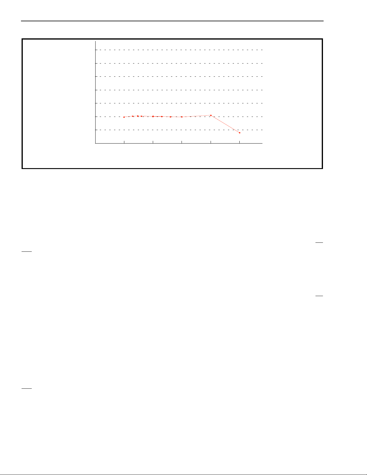
PLL Jitter Performance
To measure the intrinsic jitter of the analog PLL, the
FMIC is set to slave mode, slave to a clean MVIP C4
clock (no jitter). A resulting jitter of 0.004UI p-p is
measured on the C2o clock.
The jitter transfer function of the analog PLL, which
is the ratio of the output jitter to the input jitter, is
shown in “Figure 5 - Jitter Transfer Function of the
Analog PLL” . The measurements are made with a
controlled sinusoidal jitter modulating the MVIP C4
clock.
To measure the intrinsic jitter of the two PLLs
combined, the FMIC is set to master mode, slave to
a clean external 8kHz clock SEC8K (no jitter). A
resulting jitter of 0.206UI p-p is measured on the C2o
clock.
Jitter transfer function of the digital PLL and analog
PLL combination is determined primarily by the
digital PLL. The digital PLL is essentially a digital
sampler which samples on the nearest rising or
falling edge of its 16MHz clock and therefore has a
60ns jitter on the output.
Please note that the digital PLL and analog PLL
combination may not meet some international
standards for jitter performance. In cases where
strict idle jitter specifications must be met, an
external custom PLL may be required and the
internal analog PLL should be disabled (refer to PLL
Diagnostic section for further details).
2-152
Page 9

Preliminary Information MT90810
Local Output Clock Control
The FMIC provides four output clocks which are
always driven off of the device. The FRAME output
clock has a duty cycle and period equal to the MVIP
signal. The CLK2 and CLK4 output clocks are
F0
identical to th e MVIP C2 an d C 4
The CLK8 output provides a 8.192MHz clock. The
frame pulse and output clocks may be used to
provide framing and clocking signals to serial
interfaces other than ST-BUS, such as, GCI bus.
Timing diagrams and parameters are provided in
Figures 19 and 20 along with the associated table.
The local output clock control register is defined in
Table 11 - “Local Clock Control (LOC_CLK)
Register”. The register allows the user to program
the polarity of the four local output clocks. In
addition, the register contains four read-only bits
which indicate the logic levels on EX_8KA, EX_8KB,
DACK0
Local Serial Interface
The local serial interface is implemented on 4 input
pins LDI[0:3 ] an d fo ur ou tp u t pin s L DO[0:3]. It can b e
programmed in one of four different configurations by
setting the appropriate bits in the SER_MODE
register (refer to Figure 7 - “Serial Mode
(SER _M O DE ) Reg ist er ” ).
In serial configuration one, the data rate is set to
2Mb/s. Each input stream is associated with a serial
input pin and each serial output stream is associated
with a serial output pin. There are 32 channels per
pin.
In serial configuration two, the data rate is set to
4Mb/s. Local streams 0 and 1 are multiplexed onto
input and output pins LDI[0] and LDO[0] and streams
2 and 3 are multiplexed onto input and output pins
LDI[2] and LDO[2]. There are 64 channels per pin
and the streams are multiplexed onto the pins as
shown in Table 12 - “SER_CNFG bits (control
configuration of local serial streams)” .
In serial configuration three, the data rate is set to
8Mb/s. All four local streams are multiplexed onto
pins LDI[0] and LDO[0]. There are 128 channels per
pin and the streams are multiplexed onto the pins as
shown in Table 12 - “SER_CNFG bits (control
configuration of local serial streams)” .
In serial configuration four, the data rate is set to
2Mb/s for streams 0 and 1 and 4Mb/s for streams 2
and 3. Streams 0 and 1 are associated with serial
pins LDI/O[0] and LDI/O[1], respectively. Streams 2
and 3 are multiplexed onto pin LDI[2] and LDO[2].
The str e am s a r e m u lti p lex ed ont o t he p in s as s how n
in Table 12 - “SER_CNFG bits (control configuration
of local serial streams)” .
and DACK1 input pins of the device.
clocks, respectively.
Programmable Framing Signals
The FMIC provides two groups of independently
programmable output framing signals:
FGA[0:11] group A output framing signals are
programmed by frame start register A
(FRMA_STRT) and frame mode register A
(FRMA_MODE). FGB[0:11] group B output framing
signals are programmed by frame start register B
(FRMB_STRT) and frame mode register B
(FRMB_MODE).
The framing signals may be used to drive serial
buses interfaces other than ST-BUS.
The functional characteristics of a group of framing
output signals is controlled by MODE bits in the
frame mode register. Table 13 - “Frame Group Mode
bits” defines the various modes.
In mode 0, the frame group output depends on the
status of bits in the frame start and frame mode
registers. The values of the bits in frame start
register x (x is either A for group A or B f or group B)
are driven out on pins FGx[0:7] and the values of bits
0 to 3 in frame mode register x are driven out on pins
FGx[8:11]. This mode is selected after device reset
when all bits in both registers are cleared.
In mode 1, the first four outputs of the frame group
FGx[0:3] are available for programmed output as in
mode 0. The other 8 outputs of each frame group are
available as output drive enables for the MVIP DSI/
DSO channels within the streams. FGA4 to FGA11
outputs correspond to output drive enables for the
MVIP DSo channels within streams 0 to 7,
respectively. For example, if only two DSo channels,
0 and 2 on stream 0, are enabled then the
corresponding channels 0 and 2 on FGA4 will be
pulled low and the remaining channels will be left
high. Similarly, FGB4 to FGB11 outputs correspond
to output drive enables for the MVIP DSi channels
within strea m s 0 to 7 , re s pectively.
In mode 2, frame groups A&B are programmed as
output framing pulses for use with the local serial
data streams (refer to Figure 16 - “Frame Pulse
Timing for Mode 2” for further details). The position
of the first framing signal in a group is determined by
an 11 bit quantity. The quantity is the FMIC state
number (the number of 16MHz clock cycles during
one frame) minus one. The lower eight bits of this
quantity are located in the frame start register, and
the upper three bits are located in the frame mode
register.The width of the framing signal is determined
by the state of the FRM_TYPE bit in the frame mode
register and can be either a single bit cell time or 8
bit cell times. All framing signals in the same group
(A or B) follow each other sequentially, that is, the
first FGx[ 0] is as serted then exactl y 8 bit ce ll times
later FGx[1] is asserted and so on until the last
2-153
Page 10

MT90810 Preliminary Information
framing signal in the group is asserted. The distance
between consecutive frame pulses within a frame
group can be one 2, 4 or 8Mb/s channel time and
can be specified by two bits in the frame mode
register.
Mode 3 is identical to mode 2 except the polarity of
the framing pulses is logically inverted.
Refer to Tables 13 to 16 for details on the frame start
and frame mode registers.
All the framing signals FGA[0:11] and FGB[0:11] are
available in the 100 pin PQFP package.
Delay through the M T9081 0
Switching delay through the FMIC is dependent on
input and output stream, source and destination
channel, as well as, I/O data rate. A summary of
throughput delay values for the device is provided in
Table 1, “Throughput Delay Values” . The minimum
delay achievable in the MT90810 depends on the
data rate selected for the streams. When switching
from a slower input data rate to a faster output data
rate, the minimum delay is set by the faster output
data rate and the maximum delay is set by the
slower input data rate. When switching from a faster
input data rate to a slower output data rate, the
minimum delay is set by the slower output data rate
and the maximum delay is set by the faster input
data rate .
Input - Output
Rate
2.048 - 2.048Mb/s 2 x 2Mb/s t.s. 1 fr. + 2 x 2Mb/s t.s.
4.096 - 4.096Mb/s 3 x 4Mb/s t.s. 1 fr. + 5 x 4Mb/s t.s.
8.192 - 8.192Mb/s 5 x 8Mb/s t.s. 1 fr. + 11 x 8Mb/s t.s.
2.048 - 4.096Mb/s 3 x 4Mb/s t.s. 1 fr. + 2 x 2Mb/s t.s.
2.048 - 8.192Mb/s 5 x 8Mb/s t.s. 1 fr. + 2 x 2Mb/s t.s.
4.096 - 2.048Mb/s 2 x 2Mb/s t.s. 1 fr. + 5 x 4Mb/s t.s.
8.192 - 2.048Mb/s 2 x 2Mb/s t.s. 1 fr. + 11 x 8Mb/s t.s.
Throughput Delay
min max
Table 1 - Throug hp ut Delay Values
t.s.=timeslot is used synonymously with channel
fr.=125µs frame
2Mb/s t.s.=3.9µs
4Mb/s t.s.=1.95µs
8Mb/s t.s.=0.975µs
Initialization of the MT90810
The RESET pin should be hold low during
initialization and power-up to ensure that all internal
registers and connection and data memories are
cleared.
Microprocessor Interfa ce
The FMIC is configured and controlled via a
microprocessor interface. The microprocessor
interface consists of the combined address/data bus
AD[0:7], address bits A[0:1], the chip select bit CS
the RD
and WR signals, the address latch enable
(ALE) signal and the RDY signal. If ALE is tied to
VSS, the interface acts as an Intel nonmultiplexed
interface with the AD[0:7] bus carrying only data and
pins A[0:1] serving as the address lines. If ALE is
tied to VCC the interface acts as a Motorola
nonmultiplexed interface using A[0:1] as address
lines with RD
becoming DS and WR becoming R/W.
If ALE is active (switching during accesses), the
interface acts as in Intel multiplexed interface with
the AD[0:7] bus carrying both address and data and
the A[0:1] pins unused. The RDY signal acts as
IOCHRD Y in Intel mode an d as DTACK
in Mo torola
mode.
In all modes the FMIC decodes four read/write
registers in the microprocessor’s address space
according to Table 2, “FMIC I/O Addresses”.
Address
A[1:0]
Register
0 [00] MCS - Master Control/Status R egiste r
1 [01] LAR - Low Address Register
2 [10] AMR - Address Mode Register
3 [11] IDR - Indirect Data Register
Table 2
- FMIC I/O Addresses
The microprocessor interface provides read and
write access to all the registers. When the
microprocessor performs a read or write to the
registers, the microprocessor cycle is a fast cycle (In
Intel mode, the RDY bit is not pulled low, and in
Motorola mode, DTACK
is asserted immediately).
When the microprocessor performs a read or write to
data memory or connection memory, the
microprocessor cycle is a slow cycle (In Intel mode,
the RDY is pulled low until the cycle is complete, in
Motorola m od e D TACK
is not asserted until the cycle
is complete).
Software Control
The FMIC control registers as well as the connection
memory and data memory are accessible through
indirect addressing.
To perform a write operation to an indirect location,
the Low Address Register (LAR) and Address Mode
Register (AMR) registers must first be initialized. The
lower 8 bits of the indirect address are written to the
LAR, and then the upper bit of the indirect address
along with the appropriate bit settings to select the
,
2-154
Page 11

Preliminary Information MT90810
memory and auto increment/decrement mode is
written to the AMR. Finally, the write operation is
performed when data is written to the Indirect Data
Register(IDR). Similarly, to perform a read operation
from an indirect location, the LAR and AMR must be
initialized and then the data can be read from the
IDR.
Data memory can be read and written by the
microprocessor. This is accomplished by first
initializing the LAR and AMR register to select data
memory and then either reading from or writing to
the Indire ct D a ta R e gis te r.
Connection memory can be read and written by the
microprocessor. This is accomplished by first
initializing the LAR and AMR register to select high
or low connection memory and then either reading
from or w ritin g to th e IDR.
The indirect address can be programmed to autoincrement after reads or writes to the indirect data
register by setting bits 6 and 7 in the AMR
accordingly. The auto-increment occurs only when
the indirect address register points to either data
memory or the high byte of connection memory.
If auto-increment on read/write is enabled, and
connection memory is selected, then consecutive
reads/writes to the IDR will toggle between selection
of low to high then back to low byte of connection
memory and continue on toggling until the reads/
writes to IDR stop. Note that when reading/writing
connection memory with auto increment disabled,
the reads/w rites to IDR will toggle from low to high
byte connection memory once only.
Using the auto-increment feature, the connection
memory can be quickly initialized by resetting the
LAR and initializing the AMR for auto-increment on
write with connection memory low byte selected.
Writing a stream of bytes to IDR will then fill
connection mem ory. The first byte wr itten to t he IDR
will go to the low byte of the first connection memory
location. The memory space selection will be
automatically toggled to select connection memory
high. The second byte written to the IDR will then be
written to connection memory high of the first
connection memory location. The memory space will
automatically toggle back to the low byte connection
memory and the address pointer will be incremented
to prepare for writing to the next location in
connection memory. Similarly, the contents of
connection memory can also be read back quickly by
setting the auto-increment on read bit of AMR and
reading from the IDR continuously.
Writing to a data memory of connection memory
when the address register contains an indirect RAM
address of greater than 383 will cause unpredictable
results.
DMA In te rf ac e
The DMA interface to the FMIC is accessible only
when the microprocessor int erface is in INTEL mode.
All 128 local channels can be DMA’ed out to/in from
external memory. MVIP channels can be DMA’ed by
switching to local channels.
The DMA_EN bit in the FMIC Control/Status register
enables DMA mode. This bit should be set only after
the desired local channels have been enabled for
DMA. The DMA_EN bit does not take effect until
after the beginning of the next MVIP frame. This
assures that when th e DMA transactio ns begin, that
they begin on a frame boundary.
An individual local channel is enabled for DMA by
setting the CE bit in connection memory high for that
channel. When a channel is enabled for DMA, both
input and output are enabled for DMA. The local
output data is also driven out on the programmed
serial output stream. It is not possible to enable input
without output or vice versa. If channels in time slot
0 are enabled for DMA, there will be no DMA
requests for those channels in the first frame after
DMA is enabled. Instead, setup and preparation for
the DMA will occur in th at first frame, in the times lot
preceding. DMA transfer will actually occur in the
second frame after DMA is enabled. It is, therefore,
recommended that channels in time slot 0 not be
enabled for DMA.
The DMA signals DREQ[1] and DACK
transfers for DMA reads from the FMIC while
DREQ[0] and DACK
writes to the FMIC. For every 2Mb/s timeslot where a
channel is enabled for DMA, the FMIC will assert
DREQ and wait for a DACK
controller. Upon receiving the acknowledgement,
, it would pr oceed wit h one DMA burs t tran sfer.
DACK
DMA read requests always occur at the beginning of
the 2Mb/s time slot during which, all channels
enabled for DMA in the timeslot will be DMA’ed out in
a burst, onto the local serial data stream. One burst
implies one DREQ cycle, whereby DREQ is held low
for the duration of the transfer. The maximum
number of 8 bit channels that can be DMA’ed out
during one burst is 4, since, regardless of the serial
interface mode, there can be only four 8 bit channels
per 2Mb/s time slot, whether it be one channel per
stream (on 4 streams) at 2Mb/s, 2 channels per
stream (on 2 streams) at 4Mb/s or 4 channels all on
one stream at 8Mb/s.
DMA write requests occur at the end of the 2Mb/s
time slot during which, all channels enabled for DMA
in the timeslot will be DMA’ed from the local serial
data stream. DMA write requests can also occur in
bursts of up to four 8 bit channels. The data for write
requests is actually staggered by one DMA request
for each stream. This means that the data written
[0] control transfers for DMA
from an external
[1] control
2-155
Page 12

MT90810 Preliminary Information
into the device due to a DMA write request of a given
channel, is not actually written to that channel but to
the next channel enabled for DMA on the same
stream.
If a DMA read or write request is not completely
served by the time the next request needs to be
asserted, a DMA overrun error occurs. This causes
the corresponding overrun bit in the MCS register, as
well as, the ERR bit to be set. DMA access can be
throttled by disabling DMA for several timeslots in
between channels that have DMA enabled.
Bit Name Description (Thi s register i s clear ed up on reset)
7 PLL_UNLCK The bit will be asserted if the on-chip PLL goes out of lock. The ERR pin of the FMIC
will also be asserted high. The PLL_UNLCK bit will remai n asserted unti l a zero is
written to it.
6 DMAW_OV When a sserted, the bits indicate that a DMA overrun condition occurred on the DMA
5 DMAR_OV
4 CLK_ERR The bit monitors activity on the C4
3 MVIP_MST When set, enables the FMIC to drive the MVIP cloc k signals and consequently to
2 DMA_EN The bit should be set to enable DMA operations only after the DMA contro l registers
1 FMIC_EN W hen cleared, all MVIP signals are high impedance and LD0& 2 are set to logic 1,
0 RESET When set, clears all registers in the FMIC control space but does NOT clear connection
Read/Write channel, respectively. The ERR pin of the FMIC will also be asserted. The
DMAR/W_OV bits will remai n asserted unti l zeros are written to them.
been no activity on the C4b
high. The CLK_ERR bit will remain asserted until a zero is written to it
become master of the MVIP bus. When cleared, FMIC becomes slave of MVIP bus.
have been initialized
LD1&3 are set to logic 0. The bit should be set to enable the FMIC to drive data onto the
streams only after the chip has been initialized
and data memory. The bit must be cleared for normal operation
Table 3 - Master Control/Status Register [00]
pin for 4µs. The ERR pin of the FMIC will also be asserted
PLL Diagnostic
Diagnostic for the PLL is available via a diagnostic
register. The register contains bits which should
never be set under normal operating conditions. Two
bits in the register SEL_XIN or VCO_BYP may be
set if the user wishes to bypass the internal analog
PLL or VCO, respectively. The bits are defined in
Table 17 - “Diagnostic (DIAG_REG) Register”.
b pin of the MVIP bus and is asserted if there has
Bit Bit Function
7:0 Bits 0 to 7 of the Indirect Address
Table 4 -Low Address Register [01]
Bits Bit Function
7:6 Auto increment/d ec remen t mode
[00] Normal Mode - indirect address not auto increment ed
[01] Auto increment indirect address after indirect read of IDR
[10] Auto increment indirect address after indirect write of IDR
[11] Auto increment indirect address after indirect read or write of IDR
5:4 Selects the memory space:
[00] FMIC Control Registers
[01] Data Me mory
[10] Connection Memory Low Byte
[11] Connection Memory High Byte
3:1 Reserved
0 Bit 8 of the Indirect Address
Table 5 - Address Mode Register [10]
2-156
Page 13

Preliminary Information MT90810
Bits Bit Function
7:0 All bits are written into the indirect address locatio n specified by the LAR and AMR regist ers.
If auto increment on write/read is enabled, and connection memory is selected, then consecutive
writes/reads to/ from the IDR will tog gle between se lecti on of high byte and low byte connect ion
memory.
Table 6 - Indirect Data Register [11]
Indirect Ad dres s Name Function
0 CLK_CNTRL Clock Control Register
1 LOC_CLK Local Output Clock Control
2 SER_MO DE Local Serial Conf igurat ion Register
3 RESERVED
4 FRMA_ STRT Frame Group A start register
5 FRMA_ MO DE Frame Group A mode register
6 FRMB_ STRT Frame Group B start register
7 FRMB_ MO DE Frame Group B mode register
8:11 RESERVED
12 DIAG_REG Chip diagnostic bits
13:511 RESERVED
Table 7 - FMIC Con trol Register (read/ wr ite)
EN_SEC8K
SEL_S8K
76543210
Figure 6 - Clock Control (CLK_CNT RL) Regi ster
Name
Mode [bits] Functio n
SEL_S8K Sele cts source of 8kHz signal driven out on SEC8K pin
0 [00] Select EX_8KA as SEC8K out put
1 [01] Select EX_8KB as SEC8K out put
2 [10] Select FRAM E as SEC8K outp ut
3 [11] RESERV E D
EN_SEC8K Enables SEC8K as output
Table 8 - EN_SEC8K and SEL_S8K bits
XCLK_SELPLL_MODE
Description
2-157
Page 14

MT90810 Preliminary Information
Mode
[bits]
0 [000] X 1 divided by
1 [001] S EC8K >DPLL no frame
2 [010] E X8K A >DPLL
3 [011] EX8KB >DPLL
4 [100] MVIP C4
5 [101] SE C8K >DPLL fram e sync.
6 [110] EX8KA >DPLL frame sync.
7 [111] EX8KB >DPLL frame sync.
APLL source Frame Sync . Function
no frame
1,2, or 4
Table 9 - PLL_MODE bits (con trol PLL and fram e synch ron izati on )
sync.
sync.
frame sync.
to F0
to SEC8K
to EX8KA
to EX_8KB
Description
FMIC as Timing Master
• FMIC defaults to this mode after reset (Clock Cont rol Regist er
is cleared).
• X1 divided by 1,2 or 4 is used as the input to the APLL.
• State machine is free ru nning and does not synchronize to any
external 8kHz source.
• XCLK_SEL can be programmed to any mode.
• MVIP_MST bit in MCS is set.
• Used when the FMIC is to become the timing master in a
system which has no digital network connection s (T1 or E1).
FMIC as MVIP Master (Slaved to external 8kHz)
• DPLL is selected as the source to the APLL. Input to the DPLL
is either SEC8K,E X8KA/EX8KB.
• State machine is not synchronized to external 8kHz (SEC8K/
EX8KA/B ); that is, FRAME signal is freq locked but not
necessarily phase aligned with externa l 8kHz.
• XCLK_SEL must be programm ed to mode 0.
• MVIP_MST bit in MCS is set.
FMIC as MVIP Slav e
• FMIC is entirely slaved to MVIP bus timing.
• MVIP C4
• State machine is synchronized to MVIP C4
• MVIP_MST bit in MCS regist er must
FMIC as MVIP Master (Slaved to external 8kHz)
• DPLL is selected as the source to the APLL. Input to the DPLL
is either SEC8K,E X8KA/EX8KB.
• State machine is synchronized to external 8kHz (SEC8K/
EX8KA/B); that is, FRAM E signal is freq locked and phase
aligned with external 8kHz.
• XCLK_SEL must be programm ed to mode 0.
• MVIP_MST bit in MCS must be set.
is selected as input to APLL.
and F0 inputs.
be cleared.
Mode [bits]
X1 = Comments
0 [00] 16.384MHz X1 must be 16.384MHz when P LL is in modes 1-3 or 5-7
1 [01] 8.192M Hz
2 [10] 4.096M Hz
3 [11] RESERVED
Table 10 - XCLK_SEL bits (c on trol divide ratio of X1 cloc k)
2-158
Description
Page 15

Preliminary Information MT90810
Bit Name Bit Function
7 DACK1
6 DACK0
5 EX8KB Read-only, reads logic value on EX8KB pin
4 EX8KA Read-only, reads logic value on EX8KA pin
3 INV_CLK8 When set, inverts 8.192MHz CLK8 output pin
2 INV_CLK4 When set, inverts 4.096MHz CLK4 output pin
1 INV_CLK2 When set, inverts 2.048MHz CLK2 output pin
0 INV_FRM When set, inverts FRAME output signal
Table 11 - Local Clock Control (LOC_CLK) Register
Mode
[bits]
0 [00] 2MHz streams
All local streams are configured to run at 2MHz.
Each channel occupies a 2Mb/s timeslot of 3.9µs.
1 [01] 4MHz streams
local streams 0&1 are multip lexed ont o pin LDI/O[0]
local streams 2&3 are multip lexed ont o pin LDI/O[2]
Each channel occupies a 4Mb/s timeslot of 1.95µs.
2 [10] 8MHz streams
all four local streams are multiplexed ont o pins LDI/
O[0]
Each channel occupies a 8Mb/s timeslot of 0.975µs.
Table 12 - SER_CNFG bits (control confi gu rati on of local serial stream s )
Description
Read-only, reads logi c value on DACK1 pin
Read-only, reads logi c value on DACK0 pin
SER_CNFGRESERVED
76543210
Figure 7 - Serial Mode (SER_MODE) Register
Multiplexing of streams onto pins
LDI/O[str] where str=str eam (0-3)
2MHz,
32 channels
LDI/O[0]
(4MHz, 64
channels)
channel 0 stream 0, ch0 stream2, ch0
channel 1 stream 1, ch0 stream3, ch0
channel 2 stream 0, ch1 stream2, ch1
channel 3 stream 1, ch1 stream3, ch1
etc... .
LDI/O[0]
(8MHz, 128
channels)
channel 0 stream0, ch0
channel 1 stream1, ch0
channel 2 stream2, ch0
channel 3 stream3, ch0
channel 4 stream0, ch1
etc... .
LDI/O[0] = local stream 0
LDI/O[1] = local stream 1
LDI/O[2] = local stream 2
LDI/O[3] = local stream 3
LDI/O[2]
(4MHz, 64
channels)
2-159
Page 16

MT90810 Preliminary Information
AAAA
AAAA
AAAA
AAAA
AAAA
AAAA
AAAA
AAAA
AAAA
AAAA
AAAA
AAAA
AAAA
AAAA
AAAA
AAAA
AAAA
AAAA
AAAA
AAAA
AAAA
AAAA
AAAA
AAAA
AAA
AAA
AAA
AAA
AAA
AAA
AAA
AAA
AAA
AAA
AAA
AAA
AAA
AAA
AAA
AAA
AAA
AAA
AAA
AAA
AAA
AAA
AAA
AAA
AAAA
AAAA
AAAA
AAAA
AAAA
AAAA
AAAA
AAAA
AAAA
AAAA
AAAA
AAAA
AAAA
AAAA
AAAA
AAAA
AAAA
AAAA
AAAA
AAAA
AAAA
AAAA
AAA
AAA
AAA
AAA
AAA
AAA
AAA
AAA
AAA
AAA
AAA
AAA
AAA
AAA
AAA
AAA
AAA
AAA
AAA
AAA
AAA
AAA
Mode
[bits]
Description
3 [11] Split 2MHz/4MHz streams
Local streams 0&1 are each configured to run at
2MHz on pins LDI/O[0] and LDI/O[1], respectively.
Local streams 2&3 are multiplexed onto pin LDI/O[2].
Table 12 - SER_CNFG bits (control confi gu rati on of local serial stream s )
VARIABLE
MODE
(dependent on MODE bits)
Multiplexing of streams onto pins
LDI/O[str] where str=str eam (0-3)
LDI/O[0] = local stream 0
LDI/O[1] = local stream 1
LDI/O[2]
(4MHz, 64
channels)
channel 0 stream2, ch0
channel 1 stream3, ch0
channel 2 stream2, ch1
channel 3 stream3, ch1
etc... .
PROG_OUT(11:8)MODE [00] RESERVED
76543210
PROG_OUT(3:0)MODE [01] RESERVED
76543210
76543210
FRM_TY P E
BIT_RATE
STRTMODE [10/11]
76543210
Figure 8 - F ram e Mo de (1FRMx_M ODE ) Regist er
PROG_OUT(7:0)
MODE [00]
76543210
RESERVED
MODE [01]
76543210
MODE [10/11]
1. FRMx represents either FRMA for frame group A, or FRMB for group B.
2-160
Figure 9 - Frame Start (
STRT(7:0)
76543210
1
FRMx_STR T) Registe r
Page 17

Preliminary Information MT90810
Mode [bit s] Description
0 [00] Programmed output
1
FGx[0:11] are programmable output pins. All 8 bits of FRMx_START register are driven
out pins FGx[0:7] (with bit 0 corresponding to pin FGx[0] etc.) and bits 0-3 of
FRMx_MODE register are driven out pin FGx[8:11] (with bit 0 corresponding to pin
FGx[8] etc.).
1 [01] DS i/DS o ou tput ena bles
FGA[4:11] pins correspond to output drive enables for the M VIP DSo streams 0 to 7,
respectively.
FGB[4:11] pins correspond to output drive enables for the M VIP DSi streams 0 to 7,
respectively.
FGx[0:3] are programmable out put pins. The lea st significant four bits of FRMx_ MO DE
register are driven out pins FGx[0:3] (with bit 0 corresponding to pin FGx[0] etc.).
2 [10] Normal Framin g
Frame groups A&B (FGx[0:11]) are programmed as output framing pulses for use with
the local serial data streams ( see Figure 19 - “Fra me Pulse Timing for Mo de 2” ). The
position of the first framing signal in a group is determined by an 11 bit quantity. The
quantity is the FMIC state number minus one. The quantity determines when the first
framing signal in a group is to be asserted high.
3 [11] Inverted Framing
Identical to Normal Framing except the polarity of the framing pulses is logically inverted.
Table 13 - Frame Gro up Mode bi ts
FRMx represents either FRMA for frame group A, or FRMB for group B.
1.
Bit Name Descri ptio n
Frame Start (FRMx_S T RT) Register x
7:0 PROG_OUT(7:0) All 8 bits are driven out FGx[7:0]
Frame Mode (FRM x_MODE ) Regi ster x
7:6 MODE Frame Group Mode
0 [00] Programmed Outpu t
5:4 RES ERVED
3:0 PROG_OUT( 11:8) All 4 bits are driven out FGx[11:8]
Table 1 4 - Frame Regi ster bits fo r mod e 0
Bit Name Descri ptio n
Frame Start (FRMx_S T RT) Register x
7:0 RES ERVED
Frame Mode (FRM x_MODE ) Regi ster x
7:6 MODE Frame Group Mode
1 [01] DSi/DSo output enable
5:4 RES ERVED
3:0 PROG_OUT(3:0) All 4 bits are driven out FGx[3:0]
Table 15 - Frame Regi ster bits for mod e 1
2-161
Page 18

MT90810 Preliminary Information
Bit Name Description
Frame Start (FRMx_STRT ) Register x
7:0 STRT(7:0) Lower 8 bits of the 11 bit quantity specifi ed in Table 13 - “Frame Group
Mode bits”
Frame Mode (FRMx_STRT) Register x
7:6 MODE Frame Group Mode
2 [10] Normal Framing
3 [11] Inverted Framing
5 FRM_TYPE Type of framing signal fo r this group
0 Frame pulse is one bit cell wide
1 Frame pulse is eight bit cell wide
4:3 BIT_RATE Frame Group bit rate register
Spacing for the framing pulses is for:
0 [00] 2Mb/s da ta rate
1 [01] 4Mb/s da ta rate
2 [10] 8Mb/s da ta rate
3 [11] Reserved
2:0 STRT(11:8) Upper three bits of the 1 1 bit quantity specified in T able 13 - “Frame Group
Mode bits”
Table 16 - Frame Regis te r bits for mo des 2 &3
Bit Nam e Descri ptio n
7:3 RESERVED Should NEVER be set under norma l operating co ndit ions
2 VCO_BYP Bypass On-chip VCO
External VCO may be used in place of FMIC VCO
1 RESERVED Should NEVER be set under normal operating co ndit ions
0 SEL_XIN Select X1 as chip master clock, direct input to FMIC state machine.
Bypass entire On-chip APLL (including VC O)
Table 17 - Diagnostic (DIAG_R EG ) Regis ter
2-162
Page 19

Preliminary Information MT90810
Streams
MVIP Stream 0 0:31 0:31 0x00:0x1f
MVIP Stream 1 0:31 32:63 0x20:0x3f
MVIP Stream 2 0:31 64:95 0x40:0x5f
MVIP Stream 3 0:31 96:127 0x60:0x7f
MVIP Stream 4 0:31 128:159 0x80:0x9f
MVIP Stream 5 0:31 160:191 0xa0:0xbf
MVIP Stream 6 0:31 192:223 0xc0:0xdf
MVIP Stream 7 0:31 224:255 0xe0:0xff
Local Stream 0 0: 31 256:287 0x100:0x11f
Local Stream 1 0: 31 288:319 0x120:0x13f
Local Stream 2 0: 31 320:351 0x140:0x15f
Local Stream 3 0: 31 352:383 0x160:0x17f
Indirect RAM Address Streams Channels
decimal hex
Channels Indirect RAM Address
decimal hex
Table 18 - Data Memory Mapping
0:31 0x00:0x1f MVIP Stream 0 0:31
32:63 0x20:0x 3f MVIP Stream 1 0:31
64:95 0x40:0x 5f MVIP Stream 2 0:31
96:127 0x60:0x7f MVIP Stream 3 0:31
128:159 0x80: 0x 9f MVIP Stream 4 0:31
160:191 0xa0: 0x bf MVIP Stream 5 0:31
192:223 0xc0:0xdf MVIP Stream 6 0:31
224:255 0xe0:0xff MVIP Stream 7 0:31
256:287 0x100:0x11f Local Stream 0 0:31
288:319 0x120:0x13f Local Stream 1 0:31
320:351 0x140:0x15f Local Stream 2 0:31
352:383 0x160:0x17f Local Stream 3 0:31
Table 19 - Connectio n Mem ory Mappi ng
CAB7-0
76543210
Figure 10 - Connection Memory Low Byte
Bit Name Description
7-0 CAB7-0 Source Ch ann el Address bits 0-7. These eight bits, together with CAB8 in
connection memory high, are used to select any one of the 384 source input
channels for the connection.
Table 20 - Connectio n Mem ory Lo w Bits
2-163
Page 20

MT90810 Preliminary Information
OE/CE
RESERVED
76543210
Figure 11 - Connection Memo ry Hig h Byte
Bit Name Description
7:4 RESERVED
3DC Direction Control. controls the direction of the MVIP DSi/DS o channel pair.
When DC is set, DSi is the input channel and DSo is the output channel. When DC
is clear the direction is reversed.
2MC Message Channel. This bit, when set, will send the eight bits of connection memory
low directly out the corresponding output channel and stream. When the bit is
cleared, the contents of the progra mmed locat ion in connect ion m emory low act as
an address for the data memory and so determine the source of the corresponding
output channels and stream .
1OE Output Enable. This bit, when set, enables the output drivers on a per-channel
basis. This allows individual channels on individu al streams to be made highimpedance, permit ting the const ruction of switch mat rices. When this bit is cleared,
the drivers are disable.
0CAB8 Source Channel Address Bit 8. This bit, toget her with bits CAB 0-7 in co nnecti on
memory low, is used to select one of 384 different source input channels for the
connection.
Table 21 - Connectio n Memory High Bits for MVIP chann els
DC/CSTo
MC
CAB8
2-164
Page 21

Preliminary Information MT90810
Bit Name Description
7-4 RESERVED
3CSTo CSTo. The inverted value of this bit is output on the CSTo pin and is available for
general purpose system timing functions. The CSTo bit for each of the local output
channels is multiplexed onto the CSTo pin as illustrated below:
F0
C4
CSTo output timing
LD2:0 LD3:0LD0:0 LD1:0 LD2:1 LD3:1LD0:1 LD1:1 LD2:2 LD3:2LD0:2 LD1:2 LD0:3
2MC Message Channel. This bit, when set, will send the eight bits of connection mem ory
low directly out the corresponding output channel and stream . When the bit is cleared,
the contents of the programm ed location in connect ion me mory low act as an address
for the data memory and so determine the source of the corresponding output channels
and stream.
1CE Channel Enable. If the DMA_E N bit in the Contro l/Stat us regist er is set, then this bit
flags the control logic to perform a bidirectional DMA transfer for this input/out put
channel pair. When the bit is clear, the DMA transfer for this channel pair is disabled.
If DMA operations are not enabled then this bit must
0CAB8 S our ce Chan nel Addr ess Bit 8. This bit, together wit h bits CA B0 -7 in connection
memory low, is used to select one of 384 different source input channels for the
connection.
Table 22 - Connection Mem o ry Hig h Bits for Local chan nel s
be cleared.
2-165
Page 22

MT90810 Preliminary Information
)
JTAG Support
The FMIC JTAG interface is designed to the
Boundary-Scan standard IEEE1149.1. The standard
specifies a design-for-testability technique called
Boundary-Scan Test (BST). A boundary-scan IC has
a shift-register stage or ‘Boundary-Scan Cell’ (BSC)
in between the core logic and the I/O buffers
adjacent to each I/O pin. The BSCs can control and
observe what happens at each I/O pin of the IC. The
operation of the boundary-scan circuitry is controlled
by a Test Acce ss Port (TAP) Controller.
BOUNDARY -SCAN CELL(BSC)
BSC BSC
BSC BSC BSC BSC
BSC BSC
CORE LOGIC
T
TEST DATA IN (TDI)
A
P
C
TEST CLOCK (TCK)
O
N
T
TEST MODE
R
O
SELECT (TMS)
L
L
E
TEST DATA OUT (TDO
R
Test Ac cess P ort (TAP)
The Test Access Port (TAP) provides access to many
test supp ort function s built in to the FM IC. It con sists
of three input connections and one output
connection. The following connections form the TAP:
• Test Clo ck Input (TCK)
TCK provi des the cloc k for the t est log ic. Th e
TCK must no t inte rfere with any on-chi p cloc k
and thus rem ain i ndepe ndent . Thi s permi ts
shifting of test data into or out of the BoundaryScan register cells concurrently with the
operatio n of the dev ice wit hout inte rfering w ith
on-chip logic.
• Test Mode Select Input (TMS)
The logic s ign al (0’s and 1’s) recei ved at the
TMS input are interpreted by the TAP Controller
to control the tes t oper atio ns. Th e TMS signal s
are samp led at t he ris ing e dge of t he TCK
pulses. Wh en TM S is n ot driven from an
external source, the test logic perceives a logic
1.
Figure 12 - A Typical Boundary-Scan IC
I[0:1] Instruction Description
[00] EXTEST Boundary-Scan
register selected,
Test Enabled
This instruction is specifically provided to allo w board-level interconnect
testing of opens, bridging errors etc.
When the EXTEST instruction is selected , the on-chip logic is isolate d
from the FMIC’s I/O pin such that the value of the I/O pins is determined
by its boundary-scan register. Data for the execution of this instruction
can be preloaded into the boundary-scan register with the SAMPLE/
PRELOAD instruct ion.
[01] SAMPLE/
PRELOAD
Boundary-Scan
register selected,
Test Disabled
Two functions can be performed by the use of this instruction. It allows a
SAMPLE (‘snapshot’) of the normal operation of the FMIC to be taken for
examination. And, prior to the selecti on of another test operation, a
PRELOAD ca n place data values into the latched paral lel out put s of the
Boundary-Scan cells. During the execution of the instruction, the on-chip
logic operation is not hampered in any way.
[10] BYPASS/
TEST
Bypass register
selected,
Test Enabled
This instruction is used to BYPASS the FMIC while sampling or loading
the data registers in other devices with scan registers in the same serial
register chain. The FMIC is in test mode and the value of it’s I/O pins is
determined by its bounda ry-scan register.
[11] BYPASS/
NOTEST
Bypass register
selected,
Test Disabled
This instruction is used to BYPASS the FMIC while performing boundaryscan testing on other devices with scan registers in the sam e serial
register chain. The FMIC is allowed to function normally. This instruction
is automatically loaded upon reset of the FMIC, as spe cified in
IEEE1149.1
Table 23 - Instruction Register
2-166
Page 23

Preliminary Information MT90810
• The Test Data Input (TDI)
Serial input data applied to this port is fed either
into the instruc tion regis ter or into a test data
register, depending on the sequence previously
applied to th e TMS input. Both re gisters are
described i n a su bse quent s ecti on. The
received input data is sampled at the rising
edge of the TCK pulses. When TDI is not driven
from an extern al s ource, the test logic
perceives a l ogic 1.
• The Test Data Output (TDO)
Depending o n the s equ ence prev iousl y app lied
to the TMS input, the contents of either the
instruction re giste r or a data re gist er are
serially shifted out towards the TDO. The data
out of the TD O is c lock ed at th e falli ng edge of
the TCK pulse s. Wh en n o data is s hift ed
through the cells, the TDO driver is set to an
inactive s tate.
Instructi on R egist er
In accordance with the IEEE 1149.1 standard, the
FMIC uses public instructions listed in Table 23 “Instruction Register” . The FMIC JTAG Interface
contains a two bit instruction register. Instructions
are serially loaded into the Instruction Register from
the TDI when the TAP Controller is in its Shift-IR
state. Subsequently, the instructions are decoded to
achieve two basic functions: to select the test data
register that may operate while the instruction is
current and to define the serial test data register path
that is used to shift data between TDI and TDO
during data register scanning.
Te s t D a ta Re g iste r s
The FMIC boundary-scan register contains 84 bits.
Bit 0 in Table 24 - “Boundary Scan Register” is the
first bit clocked out. All tristate enable bits are
asserted high i.e., a logic 1 enables the
corresponding group of outputs/bidirectionals. Note
that clocking all zeros into the scan path register will
set all outpu ts to tr i state .
Bits Definition
0:11 FGB[11:0]
12:23 FGA[11:0]
24:31 DSo[7:0]
32 trista te enable for DSo[7: 0]
33:40 DSi[7:0]
41 trista te enable for DSi[7:0]
42:45 F0
46 trista te enable for
47:51 FRAME, CLK8, CLK4, CLK2, CSTo
52 trista te enable for ALL outpu t only pins
53:54 EX8KA, EX8KB
55:58 LDO[3:0]
59:62 LDI[3:0]
63:70 D[7:0]
71 trista te enable for D[7:0]
72:75 RDY, ERR, DREQ[1:0]
76:83 RD
, C4 , C2 , SEC8K
, WR, CS, ALE, A[1:0], DACK[1:0]
Table 24
- Boundary S can Re gister
As specified in the IEEE 1149.1 Standard, the FMIC
JTAG interface contains two test data registers:
• The Boundary Scan Register
The Boundary-Scan Register consists of a
series of Boundary-Scan Cells arranged to form
a scan path around the bo un dary of the cor e
logic o f t he FM IC .
• The Bypass Register
The Bypass Register is a single stage shiftregister th at prov ides a o ne-bit pa th tha t
minimizes the distance for test data shifting
from the FMIC’s TDI to its TDO.
2-167
Page 24

MT90810 Preliminary Information
Absolute Maximum Ratings*
Parameter Symbol Min Max Units
1 S upply Voltage V
2 Voltage on any I/O pin V
3 Current at outputs I
4 Storage Temperature T
DD
- V
I/O
O
S
SS
- 0.3 6 V
VSS - 0.3 VDD + 0.3 V
- 65 + 125 °C
5 Thermal Resistance Theta Ja 80 90 °C/W
* Exceeding these figures may cause permanent damage. Functional operation under these conditions is not guaranteed.
Recommended Operating Conditions
Characteristics Sym M i n Typ* Max Units Test Conditions
1Input
2 Operating Temperature T
3 Input Voltage Low V
Voltage V
DD
OP
I
* Typical figures are at 25°C and are for design aid only; not guaranteed and not subject to production testing.
DC Characteristics: Clocked operation (T
Characteristics Sym Min Typ Max Units Test Conditions
4.75 5.2 5 V
0+70°C
V
SS
=0 to 70°C; VDD=5V±5%)
OP
V
DD
mA
1 Supply Current I
2 Input High Voltage for CMOS Input s
V
3 Input Low Voltage for CMOS pins V
4 Input High Voltage for TTL Input s V
5 Input Low Voltage for TTL Inputs V
6 Low Level Input Leakage Current I
7 High Level Input Leakage Current I
8 Input Pin Capacitance C
9 Output High Voltage
10 Output Low Voltage
11 Output High Voltage
12 Output Low Voltage
V
V
V
V
13 High Impedance Leakage
14 Output Pin Capacitance C
15 Schmidt Trigger Positive Threshold
16 Schmidt Trigger Negative Threshold
DD
IH
IL
IH
IL
IL
IH
I
OH
OL
OH
OL
I
OZ
O
V
t+
V
t-
3.5 V
2V
VDD -0.4 V I
VDD -0.4 I
0.6 V
30 mA
1V
0.8 V
1.0 µ AV
1.0 µAV
4pF
VSS+0.4 V I
VSS+0.4 I
1.0 µA
10 pF
3V
= V
I
= V
I
= 4mA
OH
= 12mA
OL
= 2mA
OH
= 6mA
OL
SS
DD
2-168
Page 25

Preliminary Information MT90810
AC Electrical Characteristics- Clock and Stream Timing
Characteristics Sym Min. Typ. Max. Units Test Conditions
1 Data Propagation Delay t
2 Data Setup Time t
3 Data Hold Time t
4 Data bit 7 Tristate t
5F0b
6F0b
7F0b
/FRAME Setu p Time t
/FRAME Hold Time t
/FRAME Pulse Widt h t
8 CLK8 Period t
9 CLK8 High Width t
10 CLK8 Low Wi dth t
11 C4b
12 C4b
13 C4b
/CLK4 Period t
/CLK4 High Width t
/CLK4 Low Width t
14 C2o /CLK 2 Period t
15 C2o /CLK 2 High Width t
16 C2o /CLK 2 Low Wid th t
PD
S
H
D7
FS
FH
FW
C8P
C8H
C8L
C4P
C4H
C4L
C2P
C2H
C2L
0 30 ns Load Cap
30 ns
=200pF
For all Timing
10 ns
60 90 ns
50 150 ns
50 150 ns
200 300 ns
110 122 134 ns
55 61 67 ns
55 61 67 ns
232 244 256 ns
110 122 134 ns
110 122 134 ns
474 488 502 ns
220 244 268 ns
220 244 268 ns
16 MHz
8 MHz
t
C4P
C4b
C2o
F0b
DSO Output
DSI Output
DSO Input
DSI Input
Note: *MVIP Output streams are high impedance during the first cycle of Bit 7
t
FS
t
FW
t
C4L
t
C2H
t
FH
t
D7
t
C4H
t
C2P
t
S
t
C2L
t
PD
BIT 7* BIT 6-0
t
H
Figure 13 - M VIP Stre am Timing
2-169
Page 26

MT90810 Preliminary Information
t
FW
FRAME
CLK 8
CLK 4
CLK 2
(2 MHz
Bit Rate)
LDO
LDI
t
FS
t
FH
t
C8P
t
C8L
t
PD
t
C4L
t
C8H
t
C2L
t
C4P
t
C4H
t
C2P
t
C2H
t
S
(4 MHz
Bit Rate)
t
PD
LDO
t
S
LDI
t
(8 MHz
Bit Rate)
t
PD
H
LDO
t
S
LDI
t
H
Note: *Timing for CLK is shown for LOC_CLK register set to 00hex
Figure 14 - Local Stream Timing
16 MHz Clock
(FMIC Internal Signal)
t
H
t
PD
FGA [0:11]
FGB [0:11]
2-170
t
PD
Figure 15 - Local Frame Timing
Page 27

Preliminary Information MT90810
2042
2044
8 MHz
Clock
F0b
C4b
C2o
20460246810121416182022242628303234363840424446485052545658606264666870
DSi/
DSo Out
FGx0
FGx1
FGx0
FGx1
FGx2
FGx0
In
07
Frame Group prog ram med for 2Mb /s Data Strea ms
start of frame group can be programmed to occur on any 8 MHz clock boundary
1 bit cell
Frame Group prog ram med for 4Mb /s Data Strea ms
Frame Group prog ram med for 8Mb /s Data Strea ms
65
8 bit cells
frame pulse can be programmed to be 1 bit cell or 8 bit cells wide
43
21
07
FGx1
FGx2
Notes: x is either A for frame group A, or B for frame group B.
12 framing pulses per group, FGx0 to FGx11 are available in PQFP package.
Figure 16 - Fram e Puls e Ti ming fo r Mo de 2
2-171
Page 28

MT90810 Preliminary Information
AC Electrical Charac teri sti cs - GCI Timing
Characteristics Sym Min. Typ. Max. Units Test Conditions
1 Clock Period t
2 Clock High/Low Width t
3 Frame Setup t
4 Frame Hold t
5 Clock Edge to Data Valid t
6 Data Setup t
7 Data Hold t
FRAME
CLK4
FMIC
LDO
LDI
Figure 19 - FMIC to GCI Connections
See Detail a
CLK4/
DCL
CK
CH,
t
CL
FRS
FRH
PD
LDS
LDH
232 244 256 ns Load Cap = 200pF for all
110 122 134 ns
timi n g
50 150 ns
50 150 ns
30 ns
30 ns
10 ns
FSC
DCL
DU/DD
DU/DD
GCI
device
FRAME
FSC
DU/DD
DCL
FSC
LDO/
DU/DD
LDI/
DU/DD
/
Detail a
Ch. 31
Bit 7
t
FRS
Ch. 0
Bit 0
Note: FE=0
Ch. 0
Bit 1
Note: bit 0 identifies the most significant bit
t
t
CL
t
FRH
t
PD
CH
t
LDS
t
LDH
Ch. 0
Bit 2
t
CK
2.0V
0.8V
Ch. 0
Bit 3
2.0V
0.8V
2.0V
0.8V
2.0V
0.8V
2-172
Figure 20 - GCI Timing
Page 29

Preliminary Information MT90810
AC Electrical Charac teri sti cs - Micro pro ces sor Timing
Characteristics Sym Min. Typ. Max. Units Test Conditions
1 Address Setup t
2 Address Hold t
3 Data Access from RDY High t
4 Microprocessor Access to Data
Ready
Register (Fast) Access
Memory (Slow) Access
5 Microprocessor to RDY low t
7 Data Hold t
6 Data Setup t
8 Data Enable Off t
A[0:1 ]
t
AS
CS
t
RDY
RDY
AS
AH,
DAC
t
ACC
RDY
DH
DS
DOFF
5 ns Load Cap = 100pF for all
5ns
timi n g
25 ns
50
800
ns
ns
25 ns
5ns
5ns
20 ns
t
AH
t
AS
RD
AD[0:7]
(read)
WR
t
DS
AD[0:7]
(read)
Note:
RDY is only driven low during memory (slow) cyles.
Figure 21 - Intel Non-multiplexed Bus Timing (ALE=VSS)
t
ACC
t
DAC
t
DOFF
t
DH
2-173
Page 30

MT90810 Preliminary Information
t
AH
AD[0:7 ]
ALE
CS
RD
RDY
Notes:
RDY is only driven low during memory (slow) cyles.
is measured from either CS or RD going high, whichever is later.
t
DOFF
Add
t
AS
t
RDY
Figure 22 - Intel Multiplexed Bus Timing for Read Cycle (ALE is active)
t
ACC
Read Data
t
DAC
t
DOFF
t
AH
AD[0:7]
ALE
CS
WR
RDY
Notes:
RDY is only driven low during memory (slow cyles).
is me asured from either CS or WR going hi gh , whiche ver i s earli er.
t
DH
Add Writ e Data
t
AS
t
DAC
Figure 23 - Intel Multiplexed Bus Timing for Write Cycle (ALE is active)
t
RDY
t
ACC
t
DH
2-174
Page 31

Preliminary Information MT90810
A[0:1 ]
R/W
[WR]
DS [RD]
CS
DTACK
AD[0:7]
t
AS
t
ACC
t
DAC
Read Data
Figure 24 - Motorola Non -m ultiple xe d Bus Timing for Read Cycle (ALE=VD D)
t
AH
t
DOFF
A[0:1]
R/W
[WR]
[RD]
DS
CS
DTACK
AD[0:7]
t
AS
t
ACC
t
DS
t
AH
t
DH
Figure 25 - Motorola No n-m ul tip lexed B us Timing for Write Cycle (ALE =VD D)
2-175
Page 32

MT90810 Preliminary Information
AC Electrical Charac teri sti cs - DMA Timing
Characteristics Sym Min. Typ. Max. Units Test Conditions
1 C2o low to DACK1
2 C2o low to DACK0
3 DACK1
4 DACK0
asserted to RD low t
asserted to W R low t
asserted t
asserted t
5 C2 low to DREQ1 asserted t
6 C2 low to DREQ0 asserted t
7RD
low (on 4th DMA read pulse) to
DREQ1 removed
8WR
low (on 4th DMA write pulse) to
DREQ0 removed
9RD
8WR
pulse width (DMA=fast read) t
pulse width (DMA=fast write) t
2Mb/s timeslot (3.9µs)
F0b
CDAK1
CDAK0
DAKR
DAKW
CDRQ1
CDRQ0
t
RDRQ
t
WDRQ
RW
WW
ns
DMA
controller
dependent
ns
ns
ns
030ns
030ns
030ns
030ns
100 ns
100 ns
C2o
Detail a
t
CDAK1
DREQ1
DACK1
RD
t
DAKR
DREQ0
DACK0
WR
Note:
DMA Read and Write cycles are asynchronous to C2o.
t
DAKW
t
CDAK0
2-176
Figure 26 - DMA Interface Timing
Page 33

Preliminary Information MT90810
C2o
t
CDRQ
DREQ/1
DACK0
WR/RD
/1
async. to C2
t
RW
t
WW
t
WDRQ
t
RDRQ
Figure 27 - DMA Timing Detail A
1.008 ± 0.016
(25.6 ± 0.4)
0.787 ± 0.004
(20 ± 0.1)
80
81
51
50
100
0.106 ± 0.004
0.006 ± 0.002
(0.15 ± 0.05)
Notes:
1) Not to scale
2) Dimensions in inches
3) (Dimensions in millimeters)
(2.7 ± 0.1)
Index
1
0.026 ± 0.004
(0.65 ± 0.1)
0.012 ± 0.004
(0.30 ± 0.1)
Coplanarity: 0.006 (0.15) max.
Figure 28 - Mech anica l Data
31
30
0.110
(2.8)
0.059± 0.012
(1.5 ± 0.3)
(14 ± 0.1)
0.551 ± 0.004
0 - 12°
(19.6 ± 0.4)
0.772 ± 0.015
2-177
Page 34

MT90810 Preliminary Information
Notes:
2-178
 Loading...