

Page 1
CMOS ST-BUS FAMILY
MT9079
Advanced Controller for E1
Features
• Meets appl icabl e requi reme nts of CCIT T
G.704, G. 706, G.732, G.7 75, G. 796, I.431 a nd
ETSI ETS 300 011
• HDB3, RZ, NRZ (fibre interf ace) an d bipo lar
NRZ line code s
• Data link acce ss an d na tional bit buffers (f ive
bytes each)
• Enhanced al arms, perform anc e mon itorin g and
error insertion
• Maskable interrupts for alarms, receive CAS bit
changes, exception conditions and counter
overflow s
• Automatic in terw orking b etwe en C RC-4 and
non-CRC-4 m u lti fram in g
• Dual transm it and re cei ve 16 by te circ ular
channel b uffers
• Two frame receive elastic buffer with controlled
slip directi on ind icat ion an d 26 ch annel
hysteresi s (208 UI wande r tole rance)
• CRC-4 updating algorithm for intermediate path
points of a messa ge- based dat a link app licati on
Applications
• Primary rate ISDN netw ork node s
• Digital Access Cross-connect (DACs)
• CO and PABX switching equipment interfaces
• E1 add/dr op mu ltiple xers a nd ch annel bank s
• Test equipme nt and satel lite in terfac es
ISSUE 2 May 1995
Ordering Information
MT9079AC 40 Pin Cerami c DIP
MT9079A E 40 Pin Pl astic D IP
MT9079A L 44 Pin QFP
MT9079A P 44 Pin PLC C
-40° to 85°C
Descript io n
The MT9079 is a feature rich E1 (PCM 30, 2.048
Mbps) link framer and controller that meets the latest
CCITT and ETSI requirements.
The MT9079 will interface to a 2.048 Mbps
backplane and can be controlled directly by a
parallel processor, serial controller or through the
ST-BUS.
Extensive alarm transmission and reporting, as well
as exhaustive performance monitoring and error
diagnostic features make this device ideal for a wide
variety of applications.
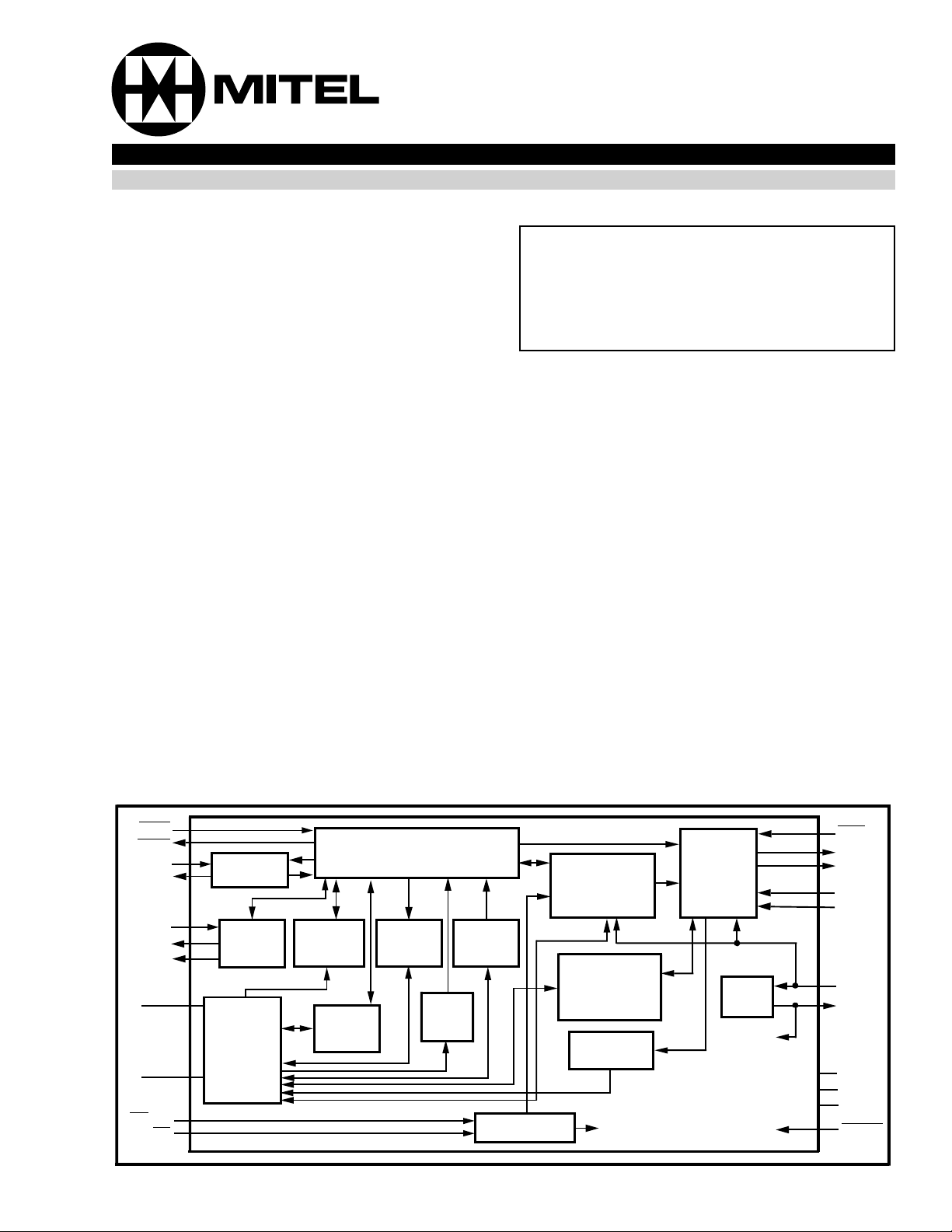
TxMF
RxMF
DSTi
DSTo
TxDL
RxDL
DLCLK
Control
Interface
(fig. 3)
C4i/C2i
F0i
Port
Data
Interface
Data
Link
Buffer
Control
Interface
National
Bit
Buffer
ABCD
Signal
Buffer
Transmit & Receive
Frame MUX/DEMUX
Test
Code
Gen.
Dual 16
Byte Tx
Dual 16
Byte Rx
Buffer
Buffer
ST-BUS Timing
2 Frame Rx
Elastic
Buffer With
Slip Control
Performance
Monitoring &
Alarm
Control
Phase
Detector
Circuit
Timin g
Figure 1 - Functional Block Diagram
PCM 30
(E1)
Link
Interface
to all registers
and counters
÷
256
Circuit
Timing
TAIS
TxA
TxB
RxA
RxB
E2i
E8Ko
V
DD
V
SS
IC
RESET
4-237
Page 2
MT9079
RESET
DSTo
RxDL
TxDL
DLCLK
D0\SIO\CSTo0
IRQ
D1
D2
D3
D4
D5
D6
D7
VDD
AC4\ST/SC
AC3
AC2
AC1
AC0
40 PIN CERDIP/PLASTIC DIP
1
2
3
4
5
6
7
8
9
10
11
12
13
14
15
16
17
18
19
20
D0\SIO\CSTo0
40
IC
39
TxA
TxB
38
37
TAIS
CSTo1
36
CSTi2
35
VSS
34
S/P
33
32
TxMF
31
RxMF
DSTi
30
29
E8Ko
28
F0i
27
RxA
RxB
26
E2i
25
C4i
24
23
DS
22
CS
21
R/W\RxD\CSTi0
IRQ
D1
D2
D3
D4
D5
D6
D7
VDD
NC
/C2i
\SCLK\CSTi1
TxDL
DLCLK
NC
65432
7
8
9
10
11
12
13
14
15
16
17
1819202122
RxDL
D0\SIO\CSTo0
DSTo
IC
RESET
4443424140
23
2425262728
NC
4443424140
D1
D2
D3
D4
D5
D6
D7
NC
CSTo1
1
2
3
4
5
6
7
8
9
10
11
1213141516
A4\ST/SC
NC
CSTi2
VSS
S/P
TxMF
RxMF
DSTi
E8Ko
F0i
RxA
RxB
AC3
AC2
AC1
44 PIN QFP
IRQ
VDD
TxA
TxB
TAIS
39
38
37
36
35
34
33
32
31
30
29
IC
RESET
3837363534
39
17
1819202122
CS
AC0
R/W\RxD\CSTi0
TxA
\SCLK\CSTi1
DS
TxB
TAIS
CSTo1
33
NC
32
CSTi2
VSS
31
S/P
30
29
TxMF
RxMF
28
DSTi
27
E8Ko
26
F0i
25
RxA
24
23
RxB
NC
E2i
/C2i
C4i
DSTo
RxDL
TxDL
DLCLK
4-238
AC3
AC2
A4\ST/SC
44 PIN PLCC
AC1
AC0
CS
R/W\RxD\CSTi0 1
\SCLK\CSTi1
DS
E2i
NC
/C2i
C4i
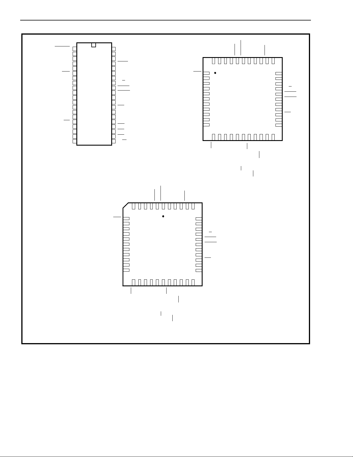
Figure 2 - Pin Connection
Page 3

Pin Description
MT9079
Pin #
DIP PLCC QFP
1 1 39 RESET RESET (Input): Low - maintains the device in a reset condition. High - normal
2240DSToData ST-BUS (Output): A 2.048 Mbit/s serial output stream which cont ains th e 3 0
3 3 41 RxDL Receive Data Link (Output): A 4 kbit/s serial stream which is demultiplexed from a
4 4 42 TxDL Transmit Data Link (Input): A 4 kbit/s serial stream which is multiplexed into a
5 5 43 DLCLK Data Link Clock (Output): A 4 kHz clock signal used to clock out DL data (RxDL) on
-644NCNo Connection.
671 IRQ
Name Description (see notes 1, 2 and 3)
operation. The MT90 79 should be reset af ter power-up. The time const ant for a
power-up reset circuit (see Figure 11) must be a minimum of five times the rise time of
the power supply. In normal operation, the RESET
of 100 nsec. to reset the device.
PCM or data channels re ceived from the PCM 30 line. See Figure 4b.
selected national bit (non-frame ali gnm ent signa l) of the PCM 30 receive signal.
Received DL data is clocked out on the rising edge of DLCLK, see Figure 20.
selected national bit (non-frame ali gnment signa l) of the P CM 30 transmi t signal.
Transmit DL data is clocked in on the rising edge of internal clock IDCLK, see Figure
21.
its rising edge. It can also be used to clock DL data in and out of external serial
controllers (i.e., MT8952). See TxDL and RxDL pin descriptions.
Interrupt Request (Outp ut): Low - interrupt request. High - no interrup t request.
is an open drain output that should be connected to VDD through a pull-up resistor .
IRQ
An active CS
signal is not required for this pin to function.
pin must be held low for a minimum
782 D0
SIO
CSTo0
[ST]
8-14 9-15 3-9 D1-D7
15 16 10 V
-1711 NCNo Connection.
16 18 12 AC4
ST/SC
[ST S]
17-2019-2213-16AC3-AC
Data 0 (Three-state I/O): The least significant bit of the bidirecti onal dat a bus of the
[P]
parallel processor interface.
Serial Input/Output (Three state I/O): This pin function is used in serial controller
[S]
mode and can be configured as control data input/ out put for Intel operat ion
to controller pin RxD). Input data is sampled LSB first on the rising edge of SCLK; data
is output LSB first on the falling edge of SCLK. It can also be configured as the control
data output for Mot orola and Nat ional Microwire operation (dat a outp ut MSB first on
the falling edge of SCLK). See CS
Control ST-BUS Zero (Output): A 2.048 Mbit/s serial status stream which provides
device status, performance mon itoring, alarm status and phase stat us data.
Data 1 to Data 7 (Three-state I/O): These signals, combined wit h D0, f orm th e
[P]
bidirectional data bus of the parallel p rocessor interface (D7 is the most significant bit).
Positive Power Supply (Input): +5V ± 10%.
DD
Address/Co ntro l 4 (Input): The most signif icant addre ss and control input for the
[P]
non-multiplexed parallel processor interfa ce.
ST-BUS/Serial Co ntrol ler (Inp u t): High - selects ST-BUS mode of operation.
Low - selects serial controller mode of ope ratio n.
Address/Control 3 to 0 (Inputs): Address and control inputs for the
0
non-multiplexed parallel processor interface. AC0 is the least significant input.
[P]
(connect
pin description.
4-239
Page 4

MT9079
Pin Description (Continued)
Pin #
DIP PLCC QFP
21 23 17 R/W
22 24 18 CS
23 25 19 DS
Name Description (see notes 1, 2 and 3)
[P]
RxD
[S]
CSTi0
[ST]
[SP]
[P]
SCLK
[S]
Read/Write (Input): High - the parallel processor is reading data from the MT9079.
Low - the parallel processor is writing data to the MT9079.
Receive Data (Input): This pin function is used in Motorola and National Microwire
serial controller mode. Data is sampled on the rising edge of SCLK, MSB first. See
pin description.
CS
Control ST-BUS Zero (Input): A 2.048 Mbit/s serial control stream which contains
the device control, mode selection, and performance monitoring control.
Chip Select (Input): Low - selects the MT9079 parallel processor or serial controller
interface. High - the parallel processor or serial controller interface is idle and all
bus I/O pins will be in a high impedance state. When controller mode is selected,
the SCLK input is sampled when CS
Intel mode; if SCLK is low it will be in Motorola/National Microwire mode. This pin
has no function (NC) in ST-BUS mode.
Data Strobe (Input): This input is the active low data strobe of the parallel
processor interface.
Serial Clock (Input): This is used in serial controller mode to clock serial data in
and out of the MT9079 on RxD and SIO. If SCLK is high when CS
device will be in Intel mode; if SCLK is low when CS
Motorola/National Microwire mode.
is brought low. If SCLK is high the device in is
goes low, the
goes low, it will be in
CSTi1
[ST]
24 26 20 C4i
25 27 21 E2i 2.048 MHz Extracted Clock (Input): This clock is extracted from the received
-2822 NCNo Connection.
26 29 23 RxB Receive B (Input): Received split phase unipolar signal decoded from a bipolar line
27 30 24 RxA Receive A (Input): Received split phase unipolar signal decoded from a bipolar line
28 31 25 F0i
29 32 26 E8Ko Extracted 8 kHz Clock (Output): An 8 kHz signal generated by dividing the
Control ST-BUS One (Input): A 2.048 Mbit/s serial control stream which contains
the per timeslot control programming.
/C2i 4.096 MH z and 2.048 MHz Sys tem Cloc k (Inp ut): This is master clock for the serial
PCM data and ST-BUS sections of the MT9079. The MT9079 automat ically det ects
whether a 4.096 or 2.048 MHz clock is being used. See Figure 22 for timing
information.
signal. Its rising edge is used internally to clock in data received on RxA and RxB.
See Figure 29.
receiver. Receives RZ and NRZ bipolar signals. See Figures 29 and 31.
receiver. Receives RZ and NRZ bipolar signals. See Figurs 29 and 31.
Frame Pulse (Input): This is the ST-BUS frame synchronization signal which
delimits the 32 channel frame of all ST-BUS streams, as well as DSTi and DSTo in
all modes.
extracted 2.048 MHz clock (E2i) by 256 and aligning it with the received PCM 30
frame. The 8 kHz signal can be used to synchronize the system clock with the
extracted 2.048 MHz clock. E8Ko is high when 8KSEL=0. See Figure 27.
30 33 27 DSTi Data ST-BUS (Input). A 2.048 Mbit/s serial stream which contains the 30 PCM or
data channels to be transmitted on the PCM 30 line. See Figure 4a.
4-240
Page 5

Pin Description (Continued)
MT9079
Pin #
DIP PLCC QFP
31 34 28 RxMF
32 35 29 TxMF
33 36 30 S/P
34 37 31 V
35 38 32 CSTi2 Control ST-BUS Input Two (Input): A 2.048 Mbit/s ST-BUS control stream which
-3933 NCNo Connection.
36 40 34 CSTo1 Control ST-BUS Output One (Output): A 2.048 Mbit/s serial status stream which
Name Description (see notes 1, 2 and 3)
Receive Multiframe Boundary (Output): An output pulse delimiting the received
multiframe bounda ry. The next frame ou tput on the dat a st ream (DSTo) is basic frame
zero on the PCM 30 link. This receive mul tiframe signal can be relat ed to either the
receive CRC multiframe (MFSEL= 1) or the receive signalling multif rame (MFS EL=0).
See Figures 25 and 26.
Transmit Multiframe Boundary (Input): This input is used to set the channel
associated and CRC transmit multiframe boundary. The device will generate its own
multiframe if this pin is held high. This input is pulled high in most applications. See
Figures 24 to 26.
Serial/P aral lel (In pu t): High - serial controll er port or ST-BUS operation.
Low - parallel processor port operation.
Negative Power Supply (Input): Ground.
SS
contains the 30 (ABCDXXXX) transmit signalling nibbles when RPSIG=0. When
RPSIG=1 thi s pin has no function. Only the most significant nibbles of each ST-BUS
timeslot are valid. See Figure 4c.
provides the 30 (ABCDXXXX) receive signalling nibbles.
37 41 35 TAIS
38 42 36 TxB Transmit B (Output): A split phase unipolar signal suitable for use with TxA, an
39 43 37 TxA Transmit A (Output):A split phase unipolar signal suitable for use with TxB, an
40 44 38 IC Internal Connection (Input): Connect to ground for normal operation.
Notes:
1. All inputs are CMOS with TTL co mpatible logic levels.
2. All outputs are CMOS and are compatible with both TTL and CMOS logic levels.
3. See AC Electrical Characteristics - Timing Parameter Measurement Voltage Levels for input and output
voltage thresholds.
Transmit Alarm Indication Signal (Input): High - TxA and TxB will transmit data
normally. Low - TxA and TxB transmits an AIS (all ones signal).
external line driver and a transformer to construct a bipolar PCM 30 line signal. This
output can also transmit RZ and NRZ bipolar signals. See Figures 28 and 30.
external line driver and a transformer to construct a bipolar PCM 30 line signal. This
output can also transmit RZ and NRZ bipolar signals. See Figures 28 and 30.
4-241
Page 6

MT9079
Functional Description
The MT9079 is an advanced PCM 30 framer that
meets or supports the layer 1 CCITT
Recommendations of G.703, G.704, G.706, G.775,
G.796 and G.732 for PCM 30; I.431 for ISDN
Primary Rate; and T1.102 f or DS1A. It also meets or
supports the layer 1 requirements of ETSI ETS 300
011 and ETS 300 233. Included are all the features
of the MT8979, except for the digital attenuation
ROM and Alternate Digit Inversion (ADI). It also
provides extensive performance monitoring data
collection features.
Control of the MT9079 is achieved through the
hardware selection of either a parallel
non-multiplexed microprocessor port, an Intel or
Motorola serial controller port, or an ST-BUS port.
The parallel port is based on the signals used by
Motorola microprocessors, but it can also be easily
mated to Intel microprocessors (see the Applications
section of this data sheet).
The serial microcontroller interface of the MT9079
will automatically adapt to either Intel or Motorola
signalling. An ST-BUS interface, consisting of two
control and one status stream, may also be selected,
however, the circular and national bit buffers cannot
be accessed in this mode.
The MT9079 supports enhanced features of the
MT8979. The receive slip buffer hysteresis has been
extended to 26 channels, which is suitable for
multiple trunk applications where large amounts of
wander tolerance is required. The phase status word
has been extended to the one sixteenth bit when the
device is clocked with C4. This provides the
resolution required for high performance phase
locked loops such as those described in MSAN-134.
A new feature is the ability to select transparent or
termination modes of operation. In termination mode
the CRC-4 calculation is performed as part of the
framing algorithm. In transparent mode the MT9079
allows the data link maintenance channel to be
modified and updates the CRC-4 remainder bits to
reflect this new data. All channel, framing and
signalling data passes through the device unaltered.
This is useful for intermediate point applications of
an PCM 30 link where the data link data is modified,
but the error information transported by the CRC-4
bits must be passed to the terminating end. See the
Application section of this data sheet.
The MT9079 has a comprehensive suite of status,
alarm, performance monitoring and reporting
features. These include counters for BPVs, CRC
errors, E-bit errors, errored frame alignment signals,
BERT, and RAI and continuous CRC errors. Also,
included are transmission error insertion for BPVs,
CRC-4 errors, frame and non-frame alignment signal
errors, and loss of signal errors.
Dual transmit and receive 16 byte circular buffers, as
well as line code insertion and detection features
have been implemented and can be associated with
any PCM 30 time slot.
A complete set of loopbacks has been implemented,
which include digital, remote, ST-BUS, payload, and
local an d rem o te time slot.
The functionality of the MT9079 has been heighten
with the addition of a comprehensive set of maskable
interrupts and an interrupt vector function. Interrupt
sources consist of synchronization status, alarm
status, counter indication and overflow, timer status,
slip indication, maintenance functions and receive
channel associated signalling bit changes.
The received CAS (Channel Associated Signalling)
bits are frozen when signalling multiframe
synchronization is lost, and the CAS debounce
duration has been extended to be compliant with
CCITT Q.422.
The MT9079 framing algorithm has been enhanced
to allow automatic interworking between CRC-4 and
non-CRC -4 interfaces. Au tomatic basic fr ame alarm
and multiframe alarms have also been added.
The national bits of the MT9079 can be accessed in
three ways. First, through single byte registers;
second, through five byte transmit and receive
national bit buffers; and third, through the data link
pins TxDL , R xD L a n d DLCLK.
4-242
The PCM 30 Interface
PCM 30 (E1) basic frames are 256 bits long and are
transmitted at a frame repetition rate of 8000 Hz,
which results in a aggregate bit rate of 256 bits x
8000/sec.= 2.048 Mbits/sec. The actual bit rate is
2.048 Mbits/sec +/- 50 ppm encoded in HDB3
format. Basic frames are divided into 32 time slots
numbered 0 to 31, see Figure 32. Each time slot is 8
bits in length and is transmitted most significant bit
first (numbered bit 1). This results in a single time
slot data r ate of 8 b i ts x 8 0 00 /s e c. = 64 kb i ts/sec.
It should be noted that the Mitel ST-BUS also has 32
channels numbered 0 to 31, but the most significant
bit of an eight bit channel is numbered bit 7 (see
Mitel Application Note MSAN-126). Therefore,
Page 7

MT9079
ST-BUS bit 7 is synonymous with PCM 30 bit 1; bit 6
with bit 2: and so on. See Figure 33.
PCM 30 time slot zero is reserved for basic frame
alignment, CRC-4 multiframe alignment and the
communication of maintenance information. In most
configurations time slot 16 is reserved for either
channel associated signalling (CAS or ABCD bit
signalling) or common channel signalling (CCS). The
remaining 30 time slots are called channels and
carry either PCM encoded voice frequency signals or
digital data signals. Channel alignment and bit
numbering is consistent with time slot alignment and
bit numbering. However, channels are numbered 1 to
30 and relate to time slots as per Table 1.
PCM 30
Timeslots
Voice/Dat a
Chann els
0 1 2 3 ....15 16 17 18 19 .... 31
X 1 2 3 . ...1 5 X 16 17 18 .... 30
Table 1 - Time slot to Chan nel Relati on shi p
Basic Frame Alignment
Time slot zero of every basic frame is reserved for
basic frame alignment and contains either a Frame
Alignment Signal (FAS) or a Non-frame Alignment
Signal (NFAS). FAS and NFAS occur in time slot
zero of consecutive basic frames as can be see in
Table 4. Bit two is used to distinguish between a FAS
(bit two = 0) and a NFAS (bit two = 1).
Basic frame alignment is initiated by a search for the
bit sequence 0011011 which appears in the last
seven bit positions of the FAS, see Frame Algorithm
section. Bit position one of the FAS can be either a
CRC-4 remainder bit or an international usage bit.
Bits four to eight of the NFAS (i.e., S
- Sa8) are
a4
national bits, which telephone authorities used to
communicate maintenance, control and status
information. A single national bit can also be used as
a 4 KHz maintenance channel or data link. Bit three,
the ALM bit, is used to indicate the near end basic
frame synchronization status to the far end of a link.
Bit position one of the NFAS can be either a CRC-4
multiframe alignment signal, an E-bit or an
international usage bit. Refer to an approvals
laboratory and national standards bodies for specific
requirements.
CRC-4 Multiframing
The primary purpose for CRC-4 multiframing is to
provide a verification of the current basic frame
alignment, although it can be used for other
functions such as bit error rate estimation. The
CRC-4 multiframe consists of 16 basic frames
numbered 0 to 15, and has a repetition rate of 16
frames X 125 microseconds/frame = 2 msec. CRC-4
multiframe alignment is based on the 001011 bit
sequence, which appears in bit position one of the
first six N FASs of a CR C -4 multiframe.
The CRC-4 multiframe is divided into two
submultiframes, numbered 1 and 2, which are each
eight basic frames or 2048 bits in length.
The CRC-4 frame alignment verification functions as
follows. Initially, the CRC-4 operation must be
activated and CRC-4 multiframe alignment must be
achieved at both ends of the link. At the local end of
a link all the bits of every transmit submultiframe are
passed through a CRC-4 polynomial (multiplied by
4
then divided by X4 + X + 1), which generates a
X
four bit remainder. This remainder is inserted in bit
position one of the four FASs of the following
submultiframe before it is transmitted, see Table 4.
The submultiframe is then transmitted and at the far
end the same process occurs. That is, a CRC-4
remainder is generated for each received
submultiframe. These bits are compared with the bits
received in position one of the four FASs of the next
received submultiframe. This process takes place in
both directions of transmission.
When more than 914 CRC-4 errors (out of a possible
1000) are counted in a one second interval, the
framing algorithm will force a search for a new basic
frame alignment. See Frame Algorithm section for
more details.
The result of the comparison of the received CRC-4
remainder with the locally generated remainder will
be transported to the near end by the E-bits.
Therefore, if E1 = 0, a CRC-4 error was discovered in
a submultiframe one received at the far end; and if
E
= 0, a CRC-4 error was discovered in a
2
submultiframe two received at the far end. No
submultiframe sequence numbers or re-transmission
capabilities are supported with layer 1 PCM 30
protocol. See CCITT G.704 and G.706 for more
details on the operation of CRC-4 and E-bits.
CAS Signall ing Mu lti fram ing
The purpose of the signalling multiframing algorithm
is to provide a scheme that will allow the association
of a specific ABCD signalling nibble with the
appropriate PCM 30 channel. Time slot 16 is
reserved for the communication of Channel
Associated Signalling (CAS) information (i.e., ABCD
signalling bits for up to 30 channels). Refer to CCITT
4-243
Page 8
MT9079
G.704 and G.732 for more details on CAS
mutliframing requirements.
A CAS signalling multiframe consists of 16 basic
frames (numbered 0 to 15), which results in a
multiframe repetition rate of 2 msec. It should be
noted that the boundaries of the signalling
multiframe may be completely distinct fro m those of
the CRC-4 multiframe. C AS multiframe alignment is
based on a multiframe alignment signal (a 0000 bit
sequence), which occurs in the most significant
nibble of time slot 16 of basic frame zero of the CAS
multiframe. Bit 6 of this time slot is the multiframe
alarm bit (usually designated Y). When CAS
multiframing is acquired on the receive side, the
transmit Y-bit is zero; when CAS multiframing is not
acquired, the transmit Y-bit is one. Bits 5, 7 and 8
(usually designated X) are spare bits and are
normally set to one if not used.
Time slot 16 of the remaining 15 basic frames of the
CAS multiframe (i.e., basic frames 1 to 15) are
reserved for the ABCD signalling bits for the 30
payload channels. The most significant nibbles are
the reserved for channels 1 to 15 and the least
significant nibbles are reserved for channels 16 to
30. That is, time slot 16 of basic frame 1 has ABCD
for channel 1 and 16, time slot 16 of basic frame 2
has ABCD for channel 2 and 17, through to time slot
16 of basic frame 15 has ABCD for channel 15 and
30.
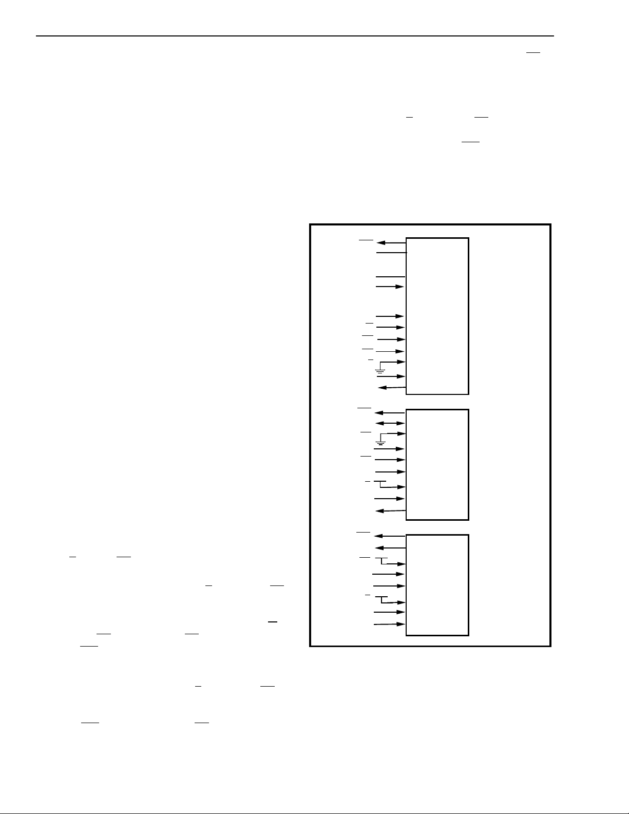
MT9079 Access and Cont rol
The Control Port Interface
The control and status of the MT9079 is achieved
through one of three generic interfaces, which are
parallel microprocessor, serial microcontroller, and
ST-BUS. This control port selection is done through
pins S/P
The parallel microprocessor port (S/P
= AC4) is non-multiplexed and consists of an eight
bit bidirectional data bus (D0-D7), a five bit
address/command bus (AC0-AC4), read/write (R/W
chip select (CS
request (IRQ
most high speed parallel microprocessors.
The serial microcontroller port (S/P = 1 and ST/SC =
0) consists of a receive data input (RxD), serial clock
input (SCLK), serial data input/output (SIO), interrupt
request (IRQ
automat ically interface to Intel, Moto rola or National
microcontrollers in either synchronous or
asynchronous modes. When controller mode is
and ST/SC.
= 0 and ST/SC
), data strobe (DS) and an interrupt
). This port can be easily interfaced to
), and chip select (CS). This port will
selected, the SCLK input is sampled when CS
brought low. If SCLK is high the device is in Intel
mode; if SCLK is low it will be in Motorola/National
Microwire mode.
The ST-BUS port (S/P
= 1 and ST/SC = 1) consists
of control streams CSTi0 and CSTi1, status stream
CSTo0, and interrupt request (IRQ
). It should be
noted that in this mode access to the circular buffers
and notional bit buffers is not provided. This port
meets the requirements of the "ST-BUS Generic
Device Specification", Mitel Application Note
MSAN-126.
PARALLEL µP
IRQ
D0
•
•
•
D7
AC4
AC0
R/W
S/P
CSTi2
CSTo1
IRQ
RxD
ST/SC
SIO
CS
SCLK
S/P
CSTi2
CSTo1
IRQ
CSTo0
ST/SC
CSTi0
CSTi1
S/P
CSTi2
),
CSTo1
CS
DS
+5V
+5V
+5V
•
•
•
CONTROL
INTERFACE
SERIAL µP
CONTROL
INTERFACE
ST-BUS
CONTROL
INTERFACE
Figure 3 - Control Port Interface
Control and Status Register Access
The parallel microprocessor and serial
microcontroller interfaces gain access to specific
registers of the MT9079 through a two step process.
First, writing to the Command/Address Register
(CAR) selects one of the 14 pages of control and
status registers (CAR address: AC4 = 0, AC3-AC0 =
is
4-244
Page 9

MT9079
don't care, CAR data D7 - D0 = page number).
Second, each page has a maximum of 16 registers
that are addressed on a read or write to a non-CAR
address (non-CAR: address AC4 = 1, AC3-AC0 =
register address, D7-D0 = data). Once a page of
memory is selected, it is only necessary to write to
the CAR when a different page is to be accessed.
See Figur e 1 7 for timing requirements.
Communications between a serial controller and
MT9079 is a two byte operations. First, a
Command/Address byte selects the address and
operation that follows. That is, the R/W
read or write function and A
determines if the next
4
byte is a new memory page address (A
data transfer within the current memory page (A
bit sel ect s a
= 0) or a
4
=
4
1). The second byte is either a new memory page
address (when A
= 0) or a data byte (when A4 = 1).
4
This is illustrated as follows:
a) Command/Address byte -
R/W XXA
4
A
3
A
2
A
1
A
0
where:
R/W - read or write operation,
X - no function,
= 0 - new memory page address to follow,
A
4
= 1 - data byte to follow, and
A
4
A
- determines the byte address.
3-A0
b) Page address or data byte -
D
D
D
D
D
D
D
7
6
5
4
3
2
D
1
0
See Figures 18 and 19 for timing requirements.
Register Access and Locations
Table 2 associates the MT9079 control and status
pages with access and page descriptions, as well as
an ST-BUS stream. When ST-BUS access mode is
used, each page contains 16 registers that are
associated consecutively with the first or second 16
channels of each ST-BUS stream. That is, page 1
regis ter lo cati ons 1 000 0 to 11111 a ppea r on CS Ti0
time slots 0 to 15, and page 2 register locations
1 0 0 0 0 t o 11111 a p pear on CSTi0 time slots 16 to 31.
It should be noted that access to the transmit and
receive circular buffers is not supported in ST-BUS
mode.
Common ST-BUS Streams
There are several control and status ST-BUS
streams that are common to all modes. CSTo1
contains the received channel associated signalling
bits (e.g., CCITT R1 and R2 signalling), and when
control bit RPSIG = 0, CSTi2 is used to control the
transmit channel associated signalling. DSTi and
DSTo contain the transmit and receive voice and
digital data. Figures 4a, b and c illustrate the relative
Page Address
D
- D
7
0
Register Description
000000 01 Master
000000 10 R/W
Control
00000011 Master
000001 00 R/W
Status
Processor/
Controller
Access
ST-BUS
Access
R/W CSTi0
RCSTo0
000001 01 Per Channel Transmit Sig nall ing R/W CSTi2
00000110 Per Cha nnel R ece ive Sign alling R CSTo1
00000111 Per Time Slot
000010 00 R/W
Control
R/W CSTi1
000010 01 Transmit Cir cular B uffer Zer o R/W --000010 10 Transmit Circular B uffer On e R /W --00001011 Receive Circular Buffer Zero R --00001100 Receive Ci rcular Buffer O ne R --00001101 Transmit National Bit Buffer R/W --00001110 Receive Nati ona l Bit Buffer R ---
Table 2 - Register Summary
4-245
Page 10

MT9079
channel positions of the ST-BUS and PCM 30
interface. See Tables 13, 14, 16 and 17 for CAS bit
positions in CSTo1 and CSTi2.
15
14
30
29
Reset Operation (Initial izati on)
The MT9079 can be reset using the hardware
RESET
pin (see pin description for external reset
circuit requirements) or the software reset bit RST
(page 1, address 11H). During the reset state, TxA
and TxB are low. When the device emerges from its
reset state it will begin to function with the default
settings described in Table 3.
Function Status
Port Selection as per pins S/P & ST/SC
Mode Termination
ST-BUS Offset 00000000*
Loopbacks Deactivated
E8Ko Deactivated
Transmit FAS C
Transmit non-FAS 1/S
Transmit MFAS (CAS) 00001111
Data Link Deactivated
CRC Interworking Activated
Code Insert/Detect Deactivated
Signalling CAS (CSTi2 & CSTo1)
ABCD Bit Debounce Deactivated
Interrupt Mask Word Zero
Interrupts
unmasked, all others
masked; interru pts not
0011011
n
1111111
n
suspended
13
28
12
27
11
26
10
25
9
24
8
23
7
22
6
21
5
20
4
19
3
18
2
17
1
0
15
14
13
12
11
10
9
8
7
16
X
15
14
13
12
11
10
9
8
7
17 18 19 20 21 22 23 24 25 26 27 28 29 30 31
CSS
RxMF Output Signalling Multiframe
Error Insertion Deactivated
Coding 10*
Tx/Rx Buffers Deactivated
Counters Random
Table 3 - Reset Status
*cleared by the RESET pin, but not by the
RST control bit.
See the Applications section for the MT9079
initialization procedure.
4-246
DSTi # 0 1 2 3 4 5 6 7 8 9 10 11 12 13 14 15 16 17 18 19 20 21 22 23 24 25 26 27 28 29 30 31
123456789101112131415
PCM 30
Timeslot #
6
6
5
5
4
4
Figure 4c - Relationship between PCM 30 Frames, Channels and CSTo1 Channels
3
3
2
2
1
1
0
X
PCM 30
channel
Basic Fr am e
Timeslot 16 for
CCS = denotes Signalling Channel if Common Channel Signalling Mode Selected
x = Unused Channel
PCM 30
0 1 2 3 4 5 6 7 8 9 101112131415SIG171819202122232425262728293031
Timeslot #
Figure 4b - Relationship between Received PCM 30 Timeslots and Output DSTo Channels
CSTo1/CSTi2 0 1 2 3 4 5 6 7 8 9 10 11 12 13 14 15 16 17 18 19 20 21 22 23 24 25 26 27 28 29 30 31
Figure 4a - Relationship between Input DSTi Channels and Transmitted PCM 30 Timeslots
DSTo 0 1 2 3 4 5 6 7 8 9 10 11 12 13 14 15 16 17 18 19 20 21 22 23 24 25 26 27 28 29 30 31
Page 11

MT9079
TAIS Ope ration
The TAIS
(Transmit AIS) pin allows the PRI interface
to transmit an all ones signal form the point of
power-up without writing to any control registers.
After the interface has been initialized normal
operation can take place by making TAIS
high.
National B it Bu ff ers
Table 4 shows the contents of the transmit and
receive Frame Alignment Signals (FAS) and
Non-frame Alignment Signals (NFAS) of time slot
zero of a PCM 30 signal. Even numbered frames
(CRC Frame # 0, 2, 4, ...) are FASs and odd
numbered frames (CRC Frame # 1, 3, 5, ...) are
NFASs. The bits of each channel are numbered 1 to
8, with 1 being the most significant and 8 the least
significant.
CRC
CRC
Frame/
Type
0/FAS C10011011
1/NFAS
2/FAS C20011011
PCM 30 Channel Zero
12345678
01ALMSa4Sa5Sa6Sa7S
a8
modes, but cannot be accessed in ST-BUS mode. In
ST-BUS mode access to the national bits can be
achieved through the Transmit and Receive
Non-frame Alignment Signal (CSTi0 and CSTo).
When selected, the Data Link (DL) pin functions
override the transmit national bit buffer function.
The CALN (CRC-4 Alignment) status bit and
maskable interrupt CALNI indicate the beginning of
every received CRC-4 multiframe.
Addre
ssable
Bytes
NBB0 S
NBB1 S
NBB2 S
NBB3 S
NBB4 S
Frames 1, 3, 5, 7, 9, 11, 13 & 15 of a CRC-4
Multiframe
F1 F3 F5 F7 F9 F11 F13 F15
a4Sa4Sa4Sa4Sa4Sa4Sa4Sa4
a5Sa5Sa5Sa5Sa5Sa5Sa5Sa5
a6Sa6Sa6Sa6Sa6Sa6Sa6Sa6
a7Sa7Sa7Sa7Sa7Sa7Sa7Sa7
a8Sa8Sa8Sa8Sa8Sa8Sa8Sa8
Table 5 - MT9079 National Bit Buffers
Note: NBB0 - NBB4 are addressa ble bytes of the MT9079
transmit and receive national bit buffers.
3/NFAS
4/FAS C30011011
5/NFAS
Sub Multi Frame 1
6/FAS C40011011
7/NFAS
8/FAS C10011011
9/NFAS
10/FAS C20011011
11/NFAS
12/FAS C30011011
13/NFAS E
Sub Multi Frame 2
14/FAS C40011011
15/NFAS E
01ALMSa4Sa5Sa6Sa7S
11ALMSa4Sa5Sa6Sa7S
01ALMSa4Sa5Sa6Sa7S
11ALMSa4Sa5Sa6Sa7S
11ALMSa4Sa5Sa6Sa7S
1 ALM Sa4Sa5Sa6Sa7S
1
1 ALM Sa4Sa5Sa6Sa7S
2
a8
a8
a8
a8
a8
a8
a8
Table 4 - FAS and NFAS Structure
indicates positio n of CRC-4 multiframe alignment signal.
Table 5 illustrates the organization of the MT9079
transmit and receive national bit buffers. Each row is
an addressable byte of the MT9079 national bit
buffer, and each column contains the national bits of
an odd numbered frame of each CRC-4 Multiframe.
Data Link Ope ration
The MT9079 has a user defined 4 kbit/sec. data link
for the transport of maintenance and performance
monitoring information across the PCM 30 link. This
channel functions using one of the national bits (S
S
, Sa6, Sa7 or Sa8) of the PCM 30 channel zero
a5
non-frame alignment signal. The S
bit used for the
a
DL is selected by making one of the bits, S
- Sa8,
a4
a4
high in the Data Link Select Word. Access to the DL
is provided by pins DLCLK, TxDL and RxDL, which
allow easy interfacing to an HDLC controller.
The 4 kHz DLCLK output signal is derived from the
ST-BUS clocks and is aligned with the receive data
link output RxDL. The DLCLK will not change phase
with a received frame slip, but the RxDL data has a
50% chance of being lost or repeated when a slip
occurs.
The TxDL input signal is clocked into the MT9079 by
the rising edge of an internal 4 kHz clock (e.g., internal
data link clo ck IDCLK ). The I DCLK is 18 0 d egrees out
of phase with the DLCLK. See Figures 20 and 21 for
timing requirements.
,
The transmit and receive national bit buffers are
selectible in microprocessor or microcontroller
4-247
Page 12

MT9079
Elastic Buffer
When control bit RDLY=0, the MT9079 has a two
frame receive elastic buffer, which absorbs wander
and low frequency jitter in multi-trunk applications.
The received PCM 30 data (RxA and RxB) is clocked
into the elastic buffer with the E2i clock and is
clocked out of the elastic buffer with the C4i
/C2i
clock. The E2i extracted clock is generated from, and
is therefore phase-locked with, the receive PCM 30
data. In normal operation, the E2i clock will be
phase-locked to the C4i
/C2i clock by an external
phase locked loop (PLL). Therefore, in a single trunk
system the receive data is in phase with the E2i
clock, the C4i
/C2i clock is phase-locked to the E2i
clock, and the read and write positions of the elastic
buffer will remain fixed with respect to each other.
In a multi-trunk slave or loop-timed system (i.e., PABX
application) a single trunk will be chosen as a network
synchronizer, which will function as described in the
previous paragraph. The rem aining trunks wil l use the
system timing derived form the synchronizer to clock
data out of t heir elastic buffe rs. Even though the P CM
30 signals from the network are synchronize to each
other, due to multiplexing, transmission impairments
and route diversity, these signals may jitter or wander
with respect to the synchronizer trunk signal. Therefore, the E2i clocks of non-synchronizer trunks may
wander with respect to the E2i clock of the synchronizer and the system bus. Network standards state
that, within limits, trunk interfaces must be able to
receive error-free data in the presence of jitter and
wander (refer to network requirements for jitter and
wander tolerance). The MT9079 will allow a minimum
of 26 channels (208 UI, unit intervals) of wander and
low frequency jitter before a frame slip will occur.
The minimum delay through the receive elasti c buffer
is approximately two channels and the maximum delay
is approximately 60 channels (RDLY=0 ), see Figure 5.
When the C4i
/C2i and the E2i clocks are not
phase-locked, the rate at which data is being w ritten
into the elastic buffer from th e PCM 30 side may differ
from the rate at which it is being read out onto the
ST-BUS. If this situation persists, the delay limits
stated in the previous paragraph will be violated and
the elastic buffer will p erform a controlled frame slip.
That is, the buffer pointers will be automatically
adjusted so that a full PCM 30 frame is either repeated
or lost. All frame slips occur on PCM 30 frame boundaries.
The RSLIP and RSLPD st atus bits gi ve indication of a
slip occurrence and direction. A maskable interrupt
is also provided.
SLPI
Figure 5 illustrates the relationship between the read
and write pointers of the receive elastic buffer.
Measuring clockwise from the write pointer, if the
read pointer comes within two channels of the write
pointer a frame slip will occur, which will put the read
pointer 34 channels from the write pointer.
Conversely, if the read pointer moves more than 60
channels from the write pointer, a slip will occur,
which will put the read pointer 28 channels from the
write pointer. This provides a worst case hysteresis
of 13 channels peak (26 channels peak-to-peak) or a
wander tolerance of 208 UI.
When control bit RDLY=1, the receive elastic buffer
becomes one frame long and the controlled slip
function is disabled. This is to allow the user to
control the receive throughput delay of the MT9079
in one of th e fo l low in g wa y s:
4-248
Read Pointer
60 CH
47 CH
34 CH
Read Pointer
Write
Pointer
512 Bit
Elastic
Store
Read Point er
13 CH
2 CH
Wander Tolerance
15 CH
-13 CH
28 CH
Read Point er
Figure 5 - Elastic Buffer Functional Diagram (208 UI Wander Tolerance)
Page 13

MT9079
1) by programming the SOFF7-0 bits to select the
desired throughput delay, which is indicated by
the phase status word bits RxTS4-0 and
RxBC2-0.
2) by controlling the position of the F0i
respect to the received time slot zero position.
The phase status word bits RxTS4-0 and
RxBC2-0 will also indicate the delay in this
application.
With RDLY=1, the elastic buffer may underflow or
overflow. This is indicated by the RSLIP and RSLPD
status bits. If RSLPD=0, the elastic buffer has
overflowed and a bit was lost; if RSLPD=1, a
underflow condition occurred and a bit was
repeated.
Framing Algorithm
The MT9079 contains three distinct, but
interdependent, framing algorithms. These
algorithms are for basic frame alignment, signalling
multiframe alignment and CRC-4 multiframe
alignment. Figure 6 is a state diagram that illustrates
these functions and how they interact.
pulse with
The MT9079 framing algorithm supports automatic
interworking of interfaces with and without CRC-4
processing capabilities. That is, if an interface with
CRC-4 capability, achieves valid basic frame
alignment, but does not achieve CRC-4 multiframe
alignment by the end of a predefined period, the
distant end is considered to be a non-CRC-4
interface. When the distant end is a non-CRC-4
interface, the near end automatically suspends
receive CRC-4 functions, continues to transmit
CRC-4 data to the distant end with its E-bits set to
zero, and provides a status indication. Naturally, if
the distant end initially achieves CRC-4
synchronization, CRC-4 processing will be carried
out by both ends. This feature is selected when
control bit AUTC
Notes for Fig u re 6 :
1) The basic frame align ment, signalling multiframe
alignment, and CRC-4 multiframe alignment
functions operate in parallel and are independent.
2) The receive channel associated signalling bits
and signalling multiframe alignment bit will be frozen
when multiframe alignment is lost.
= 0. See Figure 6 for more details.
After power-up the basic frame alignment framer will
search for a frame alignment signal (FAS) in the
PCM 30 receive bit stream. Once the FAS is
detected, the corresponding bit two of the non-frame
alignment signal (NFAS) is checked. If bit two of the
NFAS is zero a new search for basic frame alignment
is initiated. If bit two of the NFAS is one and the next
FAS is correct, the algorithm declares that basic
frame synchronization has been found (i.e., SYNC
low).
Once basic frame alignment is acquired the
signalling and CRC-4 multiframe searches will be
initiated. The signalling multiframe algorithm will
align to the first multiframe alignment signal pattern
(MFAS = 0000) it receives in the most significant
nibble of channel 16 (MFSYNC = 0). Signalling
multiframing will be lost when two consecutive
multiframes are received in error.
The CRC-4 multiframe alignment signal is a 001011
bit sequence that appears in PCM 30 bit position one
of the NFAS in frames 1, 3, 5, 7, 9 and 11 (see Table
4). In order to achieved CRC-4 synchronization two
consecutive CRC-4 multiframe alignment signals
must be received without error (CRCSYN
Figure 6 for a more detailed description of the
framing functions.
= 0). See
is
3) Manual re-framing of the receive basic frame
alignment and signalling multiframe alignment
functions can be performed at any time.
4) The transmit RAI bit will be one until basic frame
alignment is established, then it will be zero.
5) E-bits can be optionally set to zero until the
equipment interworking relationship is established.
When this has been determined one of the following
will take place:
a) CRC-to-non-CRC operation - E-bits = 0,
b) CRC-to-CRC operation - E-bits as per G.704 and
I.431.
6) All manual re-frames and new basic frame
alignment searches start after the current frame
alignment signal position.
7) After basic frame alignment has been achieved,
loss of frame alignment will occur any time three
consecutive incorrect FAS or NFAS are received.
Loss of basic frame alignment will reset the complete
framing algorithm.
4-249
Page 14
MT9079
Out of synchronization
>914 CRC errors
in one second
No CRC
multiframe alignment.
8 msec. timer expired*
CRC-4 multi-frame alignment
Start 400 msec timer.
Note 7.
YES
Search for primary basic
frame alignment signal
RAI=1, Es=0.
YES
NO
Verify Bit 2 of non-frame
alignment signal.
YES
Verify second occurrence
of frame alignment signal.
YES
Primary basic frame synchronization
acquired. Enable traffic RAI=0, E’s=0. Start
loss of primary basic frame alignment
checking. Notes 7 & 8.
NO
3 consecutive
incorrect frame
alignment
signals
NO
CRC-4 multi-frame alignment
Search for multiframe
alignment signal.
Note 7.
Start 8 msec timer.
Note 7.
Basic frame
alignment acquired
Find two CRC frame
alignment signals.
Note 7.
CRC multiframe
alignment
CRC-to-CRC interworking. Re-align to new
basic frame alignment. Start CRC-4 processing.
E-bits set as per G.704 and I.431. Indicate
CRC synchronization achieved.
Notes 7& 8.
timer expir ed **
Basic frame
alignment
acquired
No CRC
multiframe
alignment.
8 msec. timer expired*
No CRC
multiframe
alignment.
8 msec.
CRC-to-non-CRC interworking. Maintain
primary basic frame alignment. Continue to
send CRC-4 data, but stop CRC processing.
E-bits set to ‘0’. Indicate CRC-to-non-CRC
NO
Multiframe synchronization
acquired as per G.732.
NO
Check for two consecutive errored
multiframe alignment signals.
Parallel search for new basic frame
alignment signal.
Notes 6 & 7.
400 msec timer expired
operation. Note 7.
YES
Note 7.
YES
Notes 7 & 8.
* only if CRC-4 synchronization is selected and automatic CRC-4 interworking is de-selected.
** only if automatic CRC-4 interw orking is selected.
Figure 6 - Synchronization State Diagram
4-250
Page 15

MT9079
8) When CRC-4 multiframing has been achieved,
the primary basic frame alignment and resulting
multiframe alignment will be adjusted to the basic
frame alignment determined during CRC-4
synchronization. Therefore, the primary basic frame
alignment will not be updated during the CRC-4
multiframing search, but will be updated when the
CRC-4 multiframing search is complete.
Channel Signalling
When control bit TxCAS
is low the MT9079 is in
Channel Associated Signalling mode (CAS); when
TxCAS
is high it is in Common Channel Signalling
(CCS) mode. The CAS mode ABCD signalling
nibbles can be passed either via the micro-ports
(RPSIG = 1) or through related channels of the
CSTo1 and CSTi2 serial links (RPSIG = 0), see
Figure 4. Memory page five contains the receive
ABCD nibbles and page six the transmit ABCD
nibbles for micro-port CAS access.
In CAS operation an ABCD signalling bit debounce
of 14 msec. can be selected (DBNCE = 1). This is
consistent with the signalling recognition time of
CCITT Q.422. It should be noted that there may be
as much as 2 msec. added to this duration because
signalling equipment state changes are not
synchronous with the PCM 30 multiframe.
If basic frame synchronization is lost (page 3,
address 10H, SYNC
= 1) all receive CAS signalling
nibbles are frozen. Receive CAS nibbles will become
unfrozen when basic frame synchronization is
acquired.
When the SIGI interrupt is unmasked, IRQ
will
become active when a signalling nibble state change
is detected in any of the 30 receive channels. The
SIGI interrupt mask is located on page 1, address
1CH, bit 0; and the SIGI interrupt vector (page 4,
address 12H) is 01H.
b) Remote loopback (RxA and RxB to TxA and TxB
respectively at the PCM 30 side). Bit RLBK = 0
normal; RLBK = 1 activate.
MT9079
System
DSTo
Tx
PCM30
Rx
c) ST-BUS loopback (DSTi to DSTo at the system
side). Bit SLBK = 0 normal; SLBK = 1 activate.
MT9079
System
DSTi
DSTo
Tx
PCM30
d) Payload loopback (RxA and RxB to TxA and TxB
respectively at the system side with FAS and NFAS
operating normally). Bit PLBK = 0 normal; PLBK = 1
activate. The payload loopback is effectively a
physical connection of DSTo to DSTi within the
MT9079. Channel zero and the DL originate at the
point of loopback.
MT9079
System
DSTi
DSTo
Tx
PCM30
Rx
e) Local and remote time slot loopback. Remote
time slot loopback control bit RTSL = 0 normal; RTSL
= 1 activate, will loop around transmit ST-BUS time
slots to the DSTo stream. Local time slot loopback
bits LTSL = 0 normal; LTSL = 1 activate, will loop
around receive PCM 30 time slots towards the
remote PCM 30 end.
Loopbacks
In order to meet PRI Layer 1 requirements and to
assist in circuit fault sectionalization the MT9079 has
six loopback functions. These are as follows:
a) Digital loopback (DSTi to DSTo at the PCM 30
side). Bit DLBK = 0 normal; DLBK = 1 activate.
MT9079
System
DSTi
DSTo
Tx
PCM30
MT9079
System
DSTi
DSTo
Tx
PCM30
Rx
The digital, remote, ST-BUS and payload loopbacks
are located on page 1, address 15H, control bits 3 to
0. The remote and local time slot loopbacks are
controlled through control bits 4 and 5 of the per time
slot control words, pages 7 and 8.
4-251
Page 16

MT9079
PCM 30 Interfacing and Encoding
Bits 7 and 6 of page 1, address 15H (COD1-0)
determine the PCM 30 format of the PCM 30
transmit and receive signals. The RZ format
(COD1-0 = 00) can be used where the line interface
is implemented with discrete components. In this
case, the pulse width and state of TxA and TxB
directly determine the width and state of the PCM 30
pulses.
NRZ format (COD1-0 = 01) is not bipolar, and
therefore, only requires a single output line and a
single input line (i.e., TxA and RxA). This signal
along with a synchronous 4, 8 or 16 MHz clock can
interface to a manchester or similar encoder to
produce a self-clocking code for a fibre optic
transducer.
The NRZB format (default COD1-0 = 10) is used for
interfacing to monolithic Line Interface Units (LIUs).
With this format pulses are present for the full bit
cell, which allows the set-up and hold times to be
meet easily.
The HDB3
selects either HDB3 encoding or alternate mark
inversion (AMI) encoding.
control bit (page 1, address 15H, bit 5)
Bit Error Rate Counter (BR7-BR0)
An eight bit Error Rate (BERT) counter BR7 - BR0 is
located on page 4 address 18H, and is incremented
once for every bit detected in error on either the
seven frame alignment signal bits or in a selected
channel. When a selected channel is used, the data
received in this channel will be compared with the
data of the bit error rate compare word CMP7-CMP0.
See the explanation of the CDDTC control bit of the
per time slot control words (pages 7 and 8) and the
bit error rate compare word (page 2, address 11).
There are two maskable interrupts associated with
the bit error rate measurement. BERI is initiated
when the least significant bit of the BERT counter
(BR0) togg l e s, and BERO
counter value changes from FFH to 00H.
Errored Frame Alignment Signal Counter
(EFAS7-EFAS0)
An eight bit Frame Alignment Signal Error counter
EFAS7 - EFAS0 is located on page 4 address 1AH,
and is incremented once for every receive frame
alignment signal that contains one or more errors.
in initiated when the BERT
Performance Monitoring
MT9079 Error Counters
The MT9079 has six error counters, which can be
used for maintenance testing, an ongoing measure
of the quality of a PCM 30 link and to assist the
designer in meeting specifications such as CCITT
I.431 and G.821. In parallel microprocessor and
serial microcontroller modes, all counters can be
preset or cleared by writing to the appropriate
locations. When ST-BUS access is used, this is done
by writing the value to be loaded into the counter in
the appropriate counter load word (page 2, address
18H to 1FH). The counter is loaded with the new
value when the appropriate counter load bit is
toggled (page 2, address 15H).
Associated with each counter is a maskable event
occurrence interrupt and a maskable counter
overflow interrupt. Overflow interrupts are useful
when cumulative error counts are being recorded.
For example, every time the frame error counter
overflow interrupt (FERO) occurs, 256 frame errors
have been received since the last FERO interrupt.
There are two maskable interrupts associated with
the frame alignment signal error measurement. FERI
is initiated when the least significant bit of the
errored frame alignment signal counter toggles, and
FERO is initiated when the counter changes from
FFH to 00 H .
Bipolar Violation Error Counter (BPV15-BPV0)
The bipolar violation error counter will count bipolar
violations or encoding errors that are not part of
encoding. This counter BPV15-BPV0 is 16
HDB3
bits long (page 4, addresses 1DH and 1CH) and is
incremented once for every BPV error received. It
should be noted that when presetting or clearing the
BPV error counter, the least significant BPV counter
address should be written to before the most
significant location.
There are two maskable interrupts associated with
the bipolar violation error measurement. BPVI is
initiated when the least significant bit of the BPV
error counter toggles. BPVO
counter changes from FFFFH to 0000H.
is initiated when the
4-252
Page 17

MT9079
CRC Error and E-bit Counters
CRC-4 errors and E-bit errors are counted by the
MT9079 in order to support compliance with CCITT
requirements. These eight bit counters are located
on page 4, addresses 1FH and 1EH respectively.
They are incremented by single error events, which
is a maximum rate of twice per CRC-4 multiframe.
There are two maskable interrupts associated with
the CRC error and E-bit error measurement. CRCI
and EBI are initiated when the least significant bit of
the appropriate counter toggles, and CRCO and
EBO are initiated when the appropriate counter
changes fro m FFH to 0 0H .
G.821 Bit Error Rate Estimation
A G.821 BERT estimation for an E1 link can be done
with either the BERT counter, when it is associated
with the FAS, or the Errored Frame Alignment Signal
counter. It should be noted that the BERT counter
will be incremented once for every bit error found in
the FAS, and not just once for every FAS in error.
The formula for the link BERT estimation is as
follows:
BERT estimation = BERT counter value/(N*F*T)
where:
N is the number of bits verified (i.e., when the FAS
is used N = 7; when a channel is selected N = 8).
F is the number of FAS or channels in one second
(i.e., when the FAS is used F= 4000, when a
channel is selected F = 8000).
T is the elapsed time in seconds.
A similar formula can be used to provide a BERT
estimation of the transmit direction by using the E-bit
error counter, EBt.
A more accurate BERT estimation can be done using
the Bipolar Violation Error counter. The BPV error
counter will count violations that are not due to HDB3
encoding. The formula for this is as follows:
BERT estimation = BPV Error counter value/(256*8000*T)
where:
256 is the number of bits per basic frame.
8000 is the number of basic frames in one second.
T is the elapsed time in seconds.
This assumes that one BPV error will be the result of
one bit error.
RAI and Continuous CRC-4 Error Counter
When the re ceive Remote Alarm Indic ation is activ e
(RAI = 1 - bit 3 of the NFAS) and a receive E-bit
indicates a remote error (En = 0), the RCRC counter
will be incremented. This counter will count the
number of submultiframes that were received in error
at the remote end of a link during a time when layer
one capabilities were lost at that end. This eight bit
RCRC counter is located on page 4, addresses 19H.
There are two maskable interrupts associated with
the RCRC counter. RCRI is initiated when the least
significant bit of the RCRC counter toggles, and
RCRO and EBO are initiated when the counter
changes from FFH to 00H.
A similar formula can be used with the FAS error
counter.
BERT estimation = FAS Error counter value/(7*4000*T).
The CRC-4 error counter can also be used for BERT
estimation. The formula for BERT estimation using
the CRC-4 e rr o r c o unt is as fo llows:
BERT estimation = CEt counter value/(2048000*T)
where:
2048000 is the number of bits that are
received in one second.
T is the elapsed time in seconds.
Maintenance and Alarms
Error Insertion
Five types of error conditions can be inserted into the
transmit PCM 30 data stream through control bits,
which are located on page 2, address 10H. These
error events include the bipolar violation errors
(BPVE), CRC-4 errors (CRCE), FAS errors (FASE),
NFAS errors (NFSE), and a loss of signal condition
(LOSE). The LOSE function overrides the HDB3
encoding function.
4-253
Page 18

MT9079
Circ ular Buf f ers
The MT9079 is equipped with two 16 byte circular
receive buffers and two 16 byte circular transmit
buffers, which can be connected to any PCM 30 time
slot. Connection is made through control bits 3 to 0
of the per time slot control words on pages 7 and 8.
These buffers will transmit and receive time slot data
synchronously with the CRC-4 multiframe.
Transmit circular buffer zero is located on page 9
(TxB0.0 to TxB0.15) and transmit circular buffer one
is located on page 10 (TxB1.0 to TxB1.15).
The two circular 16 byte receive buffers (page 11 RxB0.0 to RxB0.15 and page 12 - RxB1.0 to
RxB1.15) record the data received in an associated
channel for the next 16 frames beginning with the
CRC-4 multiframe boundary. T he assigned channel
data from the next multiframe will over-write the
current data until the buffer is disconnected.
The STOP and START maskable interrupts extend
the normal operation of the receive buffers in the
following manner.
(CDW) and Detect Word Mask (CDM) mentioned
below.
b) START - once activated, receive circular buffer 0
or 1 begins recording time-slot data and initiates an
interrupt when a user-defined eight bit pattern is
received. This user-defined bit pattern is determined
by the Code Detect Word (CDW) and Detect Word
Mask (CDM) mentioned below.
The functionality and control of the START and
STOP interrupts is described in Table 6.
PCM 30 Time-Slot Code Insertio n and Detectio n
Idle line codes, flags or user-defined codes can be
inserted and de tected on any com bination of PCM 30
time-slots. This is done as follows:
a) CIW7-0 - Code Insert Word 7 to 0 (page 1, address
17H) is an eight bit code that is transmitted on
user-defined PCM 30 time-slots. Transmit time-slots
are selected through bit 7 of the per time slot control
words (pages 7 and 8).
a) STOP - once activated, receive circular buffer 0 or
1 records time-slot data until that data either
matches or mismatches a user-defined eight bit
pattern, then the interrupt occurs. This user-defined
bit pattern is determined by the Code Detect Word
Interrupt
Mask
STOP
(page 1,
address
1EH, bit 2)
Function*
(note 3)
STOP0 Circular bu ffer zero st ops rec ordin g on a m atch with CD W and CDM.
STOP1 Circular buffer on e stop s recordi ng on a m atch with CDW and CDM .
STOP0
Circular buffer zer o stop s recor ding on a misma tch wit h CDW an d
CDM.
STOP1
Circular buffer on e stop s reco rding on a m ism atch wit h CDW an d
CDM.
START
(page 1,
address
1EH, bit 1)
START0 Circular buffer zer o starts recordi ng on a match wi th CDW and CD M.
START1 Circular buffer on e starts re cord ing on a match wi th CDW an d CD M.
START0
Circular buffer zer o starts recordi ng on a mismat ch with CDW and
CDM.
b) CDW7-0 - Code Detect Word 7 to 0 (page 1,
address 18H) is an eight bit code, which is compared
with the contents of user-defined PCM 30 receive
time-slots. When the contents of the selected channels
matches the CDW7-0 the DATA interrupt, if unmasked,
will be triggered. Receive time-slots are selected
Description (see notes 1 and 2)
START1
Circular buffer on e starts re cord ing on a misma tch with CDW and
CDM.
Table 6 - START and STOP Interrupt Control
Notes:
1) The interrupt vector value associated with these interrupts is 02H (page 4, address 12H)
2) The START and STOP interrupts can be used to record the data between two pre-defined eight bit data patterns received in a
particular pattern.
3) Circular Buffer Accumulate Control Word (page 2, address 12H).
4-254
Page 19

MT9079
through bit 6 of the per time slot control words (pages
7 and 8).
c) DWM7-0 - Detect Word Mask 7 to 0 (page 1,
address 19H) is an eight bit code, which determines
the bits that will be considered in the comparison
between the receive dat a and the Code Detect Word
(CDW7-0). If one, the bit position will be included - if
zero, the bit position will be excluded.
The DATA interrupt vector value is 02H located on
page 4 address 12H.
Alarms
The MT9079 will detect and transmit the following
alarms:
a) Remote Alarm Indication - bit 3 (ALM) of the receive
NFAS;
b) Alarm Indication Signal - unframed all ones signal
for at least a double frame (512 bits) or two double
frames (1024 bits);
signal to the far end of the link. Th is transmission will
cease when signalling multiframe alignment is
acquired.
Interrupt
Category and
Interrupt De scription
Vector
Synchronization
D7 D0
10000000
Alarm
D7 D0
01000000
Counter Indication
D7 D0
00100000
- Loss of Synchronization.
SYNI
MFSYI - Loss of Multiframe Sync.
CSYNI - Loss of CRC-4 Sync.
RFALI - Remote CRC-4 Fail.
YI - Remote Multiframe Sync. Fail.
- Remote Alarm Indication.
RAII
AISI
- Alarm Indication Signal.
AIS16I
- AIS on Channel 16.
- Loss of Signal.
LOSI
AUXPI - Auxiliary Pattern.
EBI - Receive E-bit Error.
CRCI - CRC-4 Error.
CEFI - Consecutive Errored FASs.
FERI
- Frame Alignment Signal Error.
BPVI - Bipolar Violation Error.
RCRI - RAI and Continuous CRC Error.
BERI - Bit Error.
c) Channel 16 AIS - all ones signal in channel 16;
d) Auxiliary patte rn - 101010. .. pattern for at least 512
bits;
e) Loss of Signal - a valid loss of signal condition
occurs when there is an absence of receive PCM 30
signal for 255 contiguous pulse (bit) positions from the
last received pulse. A loss of signal condition will
terminate when an average ones density of at least
12.5% has been received over a period of 255
contiguous pulse positions starting wit h a pulse; a nd
f) Remote Sig nalling Multifram e Alarm - bit 6 (Y-bit) of
the multiframe alignment signal.
Automatic Alarm s
The transmission of RAI and signalling multiframe
alarms can be made to function automatically from
control bits ARAI
When ARAI
lost (SYNC
and AUTY (page 1, address 11H).
= 0 and basic frame synchronization is
= 1), the MT9079 will automatically
transmit the RAI alarm signal to the far end of t he link.
The transmission of this alarm signal wil l cease when
basic frame alignment is acquired.
When AUTY
not acquired (MFSYNC
= 0 and signalling multiframe alignment is
= 1), the MT9079 will
automatically transmit the multiframe alarm (Y-bit)
Counter O verfl ow
D7 D0
00010000
One Second
D7 D0
00001000
SLIP
D7 D0
00000100
Maintenance
D7 D0
00000010
Signalling
D7 D0
00000001
EBO - Receive E-bit Error.
CRCO - CRC-4 Error.
FERO - Frame Alignment Signal.
- Bipolar Violation.
BPVO
RCRO - RAI and Continuous CRC Error.
BERO - Bit Error
1SECI - One Second Timer.
CALNI - CRC-4 Multiframe Alignme nt.
- Receive Slip.
SLPI
STOP - Stop Accumulating Data.
STRT - Start Accumulating Data.
DATA - Data Match.
SIGI - Receive Signalling Bit Change.
Table 7 - MT9079 Interrupt Vectors (IV7-IV0)
Interrupts
The MT9079 has an extensive suite of maskable
interrupts, which are divided into eight categories
based on the type of event that caused the in terrupt.
Each interrupt category has an associated interrupt
vector described in Table 7. Therefore, when
unmasked interrupts occur, IRQ
will go low a nd one or
more bits of the interrupt vector (page 4, address 12H)
will go high. In processor and controller modes after
4-255
Page 20

MT9079
the interrupt vector is read it is automatically cleared
and IRQ
ST-BUS mode, as well as processor and controller
modes, this function is accomplished by toggling the
INTA bit (page 1, address 1AH. )
All the interrupts of the MT9079 are maskable. This i s
accomplished through interrupt mask words zero to
four, which are located on page 1, addresses 1BH to
1EH.
After a MT9079 reset (RESET
all interrupts of mask words one, two and three are
masked; and the interrupts of mask word zero are
unmasked.
Interrupt Mask Word Zero
will return to a high impedance state. In
pin or RST control bit)
Bit 7 Bit 0
SYNI RAII AISI AIS16I LOSI FERI BPVO SLPI
Control and Status Registers
Interrupt Mask Wor d One
Bit 7 Bit 0
EBI CRCI CEFI BPVI RCRI BERI --- SIGI
Interrupt Mask Wor d Two
Bit 7 Bit 0
EBO CRCO CALNI FERO RCRO BERO AUXPI ---
Interrupt Mask Wor d Three
Bit 7 Bit 0
MFSYI CSYNI RFALI YI 1SEC STOP STRT DATA
All interrupts may be suspended, without changing
the interrupt mask words, by making the SPND
control bit of page 1, address 1AH high.
Address
(A
4A3A2A1A0
10H (Table 25) Multiframe, Nation al Bit Buffer and Data
11H (Table 26) Mode Selection TIU0, CRCM, RST, ARAI, AUTY, MO D E,
12H (Table 27) Transmit Non-frame Alignment Signal TIU1, TALM & TNU4-8
13H (Table 28) Transmit Multiframe Alignment Signal TMA1-4, X1, Y, X2 & X3
14H (Table 29) ST-BUS Offset SOFF7 - SOFF0
15H (Table 30) Coding and Loopback Control Word COD1-0, HDB3
16H (Table 31) Transmit Alarm Control TAIS, TAIS0, TAIS16, TE, REFRM, 8KSE L,
17H (Table 32) Code Insert Word CIW7 - CIW0
18H (Table 33) Code Detect Word CDW7 - CDW0
19H (Table 34) Code Detect Bit Mask DWM7 - DWM0
1AH (Table 35) Interrupt , Signall ing and BERT Control
1BH (Table 36) Interrupt Mask Word Zero SYNI, RAII, AISI, AIS16I, LOSI, FERI, BPVO
)
Link Selection
Word
Register Function
ASEL, MFSEL, NBTB & S
CSYN
& AUTC
PLBK
CIWA & CDWA
RDLY, SPND, INTA,TxCAS
& SLPI
, MFRF, DLBK, RLBK, SLBK &
- S
a4
a8
, RPSIG & BFAS
1CH (Table 37) Interrupt Mask Word One EBI, CRCI, CEFI, BPVI, RCRI, BERI & SIGI
1DH (Table 38) In terrupt Mask Word Two EBO, CRCO, CALNI, FERO, RCRO, BERO &
AUXPI
1EH (Table 39) Interrupt Mask Word Three MFSYI, CSYNI, RFALI, YI, 1SEC, STOP,
STRT & DAT A
1FH Unused. ---
Tabl e 8 - Master Control Words (Page 1)
4-256
Page 21

MT9079
Address
(A
4A3A2A1A0
10H (Table 40) Error and Debounce Selection Word BPVE, CRCE, FASE, NFSE, LOSE & DBNCE
11H (Table 41) Bit Error Rate Compare Word CMP7 - CMP0
12H (Table 42) Circular Buffer Accumulate Control Word START0
13H - 14H Unused. --15H (Table 43) Counter Load Control Word LDCRC, LDEC, LDBPV, LDEF, LDRC &
16H - 17H Unused. --18H (Table 44) Bit Error Rate Load Word BRLD7 - BRLD0
19H (Table 45) RAI and Continuous CRC Error Counter
1AH (Table 46) Errored Frame Alignment Load Word EFLD7 - EFLD0
1BH Unused. --1CH (Table 47) Mo st Signif icant Bipolar Violat ion Load
1DH (Table 48) Least Significa nt Bipola r Violation Load
)
Load Word
Word
Word
Register Function
, START0, START1, START1,
STOP0
LDBER
RCLD7 - RCLD0
BPLD15 - B PLD8
BPLD7 - BPLD0
, STOP0, STOP 1 & STOP1
1EH (Table 49) E-bit Er ror Counter Load Word ECLD7 - ECLD0
1FH (Table 50) CRC-4 Error Count er Load Word CCLD7 - CCLD0
Tabl e 9 - Master Control Words (Page 2)
Address
(A
4A3A2A1A0
10H (Table 51) Synchronization St atus Word SYNC
11H (Table 52) Receive Frame Alignment Signal RIU0 & RFA2-8
12H (Table 53) Time r Status Word 1SEC, 2SEC, CRCT, EBT, 400T, 8T & CALN
13H (Table 54) Receive Non-frame Alignment Signal RIU1, RNFAB, RALM & RNU4-8
14H (Table 55) Receive Multiframe Alignm ent Sig nal RMA1 -4, X1 , Y, X2 & X3
15H (Table 56) Most Significant Phase Status Word RSLIP, RSLPD, AUXP, CEFS, RxFRM &
16H (Table 57) Least Significant Phase Status Word RxTS1-0, RxBC2-0 & RxEB2 -0
17H - 18H Unused. --19H (Table 58) Alarm Status Word One CRCS1, CRCS2, RFAIL, LOSS, AIS16S,
)
Regist er Fu ncti on
, MFSYNC , CRCS YN, REB1, REB2,
CRCRF, PSYNC & CRCIWK
RxTS4-2
AIS S, RA IS & R CRS
1AH - 1FH Unused. ---
Table 10 - Master Status Words (Page 3)
4-257
Page 22

MT9079
Address
(A
4A3A2A1A0
)
Register Function
10H - 11H Unused. --12H (Table 59) Interrupt Vector IV7 - IV0
13H - 17H Unused --18H (Table 60) Bit Error Rate Counter BR7 - BR0
19H (Table 61) RAI and Continuous CRC Error Counter RCRC7 - RCRC0
1AH (Table 62) Errored Frame Alignment Signal Counter EFAS7 - EFAS0
1BH Unused. --1CH (Table 63) Mo st Signif icant Bipolar Violat ion E r ror
BPV15 - BPV8
Counter
1DH (Table 64) Least Significa nt Bipola r Violation Error
BPV7 - BPV0
Counter
1EH (Table 65) E-b it Error Counter E Bt EC7 - EC0
1FH (Table 66) CRC-4 Error Count er CEt CC7 - CC0
Table 11 - Master Status Words (Page 4)
Per Channel Transmit Signalling (Page 5)
and Table 14 describes the function of ST-BUS time
slots 17 to 31 of CSTi2.
Table 12 describes Page 05H, addresses 10001 to
11111, which cont ains the T ransmit Si gnalling Control
Words for PCM 30 channels 1 to 15 and 16 to 30.
Control of these bits is through the processor or
controller port when the RPSIG bit is high.
After a RESET
or RST function, this page will be
deselected (CSTi2 selected). RPSIG must be made
high before the page can be programmed.
Bit Name Functional Description
7 - 4
3 - 0
A(n),
B(n),
C(n)
&
D(n)
A(n+15),
B(n+15),
C(n+15)
&
D(n+15)
Transmit Signalling Bits for Channel
n. These bits are transmitted on the
PCM 30 2048 kbit/sec. link in bit
positions one to four of time slot 16 in
frame n (where n = 1 to 15), and are
the A, B, C, D signalling bits associated with channel n.
Transmit Signalling Bits for Channel
n + 15. These bits are transmitted on
the PCM 30 2048 kbit/sec. link in bit
positions five to eight of time slot 16
in frame n (where n = 1 to 15), and
are the A, B, C, D signalling bits
associated with channel n + 15.
Table 12 - Transmit Channel Associated Signalling
(Pag e 5)
Bit Name Functional Description
7 - 4 A(n),
B(n),
C(n)
&
D(n)
3 - 0 --- Unused.
Transmit Signalling Bits for Channel
n. These bits are transmitted on the
PCM 30 2048 kbit/sec. link in bit
positions one to four of time slot 16 in
frame n (where n = 1 to 15), and are
the A, B, C, D signalling bits asso ciated with channel n.
Table 13 - Transmit CAS Channels 1 to 15 (CSTi2)
Bit Name Functional Description
7 - 4 A(n+15),
B(n+15),
C(n+15)
&
D(n+15)
3 - 0 --- Unused.
Transmit Signalling Bits for Channel
n + 15. These bits are transmitted on
the PCM 30 2048 kbit/sec. link in bit
positions five to eight of time slot 16
in frame n (where n = 1 to 15), and
are the A, B, C, D signalling bits
associated with channel n + 15.
Table 14 - Transmit CAS Channels 16 to 30 (CSTi2)
Serial per channel transmit signalling control through
CSTi2 is selected when RPSIG is low. Table 13
describes the function of ST-BUS time slots 1 to 15,
4-258
Page 23

MT9079
Per Channel Receive Signalling (Page 6)
Page 06H, addresses 10001 to 11111 contain the
Receive Signalling Control Words for PCM 30
channels 1 to 15 and 16 to 30.
Bit Name Functional Description
7 - 4 A(n),
B(n),
C(n)
&
D(n)
3 - 0 A(n+15),
B(n+15),
C(n+15)
&
D(n+15)
Receive Signalling Bits for Channel
n. These bits are received on the
PCM 30 2048 kbit/sec. link in bit
positions one to four of time slot 16 in
frame n (where n = 1 to 15), and are
the A, B, C, D signalling bits associated with channel n.
Receive Signalling Bits for Channel n
+ 15. These bits are received on the
PCM 30 2048 kbit/sec. link in bit
positions five to eight of time slot 16
in frame n (where n = 1 to 15), and
are the A, B, C, D signalling bits
associated with channel n + 15.
Table 15 - Receive Channe l Associated Signalli ng
(Pag e 6 )
Serial per channel receive signalling status bits
appear on ST-BUS stream CSTo1. Table 16
describes the function of ST-BUS time slots 1 to 15,
and Table 17 describes the function of ST-BUS time
slots 17 to 31 of CSTo1.
Bit Name Functional Description
7 - 4 A(n),
B(n),
C(n)
&
D(n)
3 - 0 ---
Receive Signalling Bits for Channel
n. These bits are received on the
PCM 30 2048 kbit/sec. link in bit
positions one to eight of time slot 16
in frame n (where n = 1 to 15), and
are the A, B, C, D signalling bits
associated with channel n.
Unused - high output level.
Table 16 - Receive CAS Channel s 1 to 15 (CSTo1)
Bit Name Functional Description
7 - 4 A(n+15),
B(n+15),
C(n+15)
&
D(n+15)
Receive Signalling Bits for Channel n
+ 15. These bits are received on the
PCM 30 2048 kbit/sec. link in bit
positions five to eight of time slot 16
in frame n (where n = 1 to 15), and
are the A, B, C, D signalling bits
associated with channel n + 15.
Per Time Slot Control Words (Pages 7 and 8)
The control functions described by Table 18 are
repeated for each ST-BUS time slot. When ST-BUS
access is selected, the programmed CSTi1 time slot
corresponds to the controlled ST-BUS or PCM 30
time slot. It should be noted that the two receive and
two transmit circular buffers are not accessible in
ST-BUS mode.
In processor and controller modes, pages 7 and 8
contain the 32 per time slot control words. Page 7
addresses 10 000 to 11111 correspond to time slot s 0
to 15, while page 8 addresses 10000 to 11111
correspond to time slots 16 to 31. These control bits
are not cleared by the RESET
or RST reset
functions.
Bit Name Functional Descriptio n
7 CDIN Code Insert Activation. If one, the
data of CIW7-0 is transmitted i n the
corresponding PCM 30 time slot. If
zero, the data on DSTi is transmitted
on the corresponding PCM 30 time
slot.
6 CDDTC Code Detect Activation. If one, the
5 RTSL Remote Time Slot Loopback. If one,
4 LTSL Local Time Slot Loopback. If one, the
data received on the corresponding
PCM 30 time slot is compared with
the unmasked bits of the code detect
word. When the DATA interrupt is
unmasked and this positive match is
made, an interrupt wil l be initiate d. If
zero, the data is not be compared to
the unmasked bits of the code detect
word.
the corresponding PCM 30 receive
time slot is looped to the corre sponding PCM 30 transmit time slot. This
received time slot will also be present
on DSTo. An ST-BUS offset may
force a single frame delay . If zero, the
loopback is disabled.
corresponding transmit time slot is
looped to the corresponding receive
time slot. This transmit time slot will
also be present on the transmit PCM
30 stream. An ST-BUS offset may
force a single frame delay. If zero,
this loopback is disabled.
3 - 0 ---
Unused - high output level.
Tabl e 17 - Receive CAS Ch ann els 17 to 31 (CSTo1)
Table 18 - Per Time Slot Con trol Words
(Pages 7 and 8) (continued)
4-259
Page 24

MT9079
.
Bit Name Functional Description
3 TBUF0 Transmit Buffer Zero Connect. If one,
the contents of the transmit circular
buffer zero will be tran smitted in the
corresponding time slot beginning at
the next multiframe boundary. If zero,
circular buffer zero is not connected
to this time slot. T his buffer is accessible only in processor and controller
modes.
2 TBUF1 Transmit Buffer One Connect. If one,
the contents of the transmit circular
buffer one will be transmitted in the
corresponding time slot beginning at
the next multiframe boundary. If zero,
circular buffer one is not connected
to this time slot. T his buffer is accessible only in processor and controller
modes.
1 RBUF0 Receive Buffer Zero Connect. If one,
the data of the corresponding receive
time slot will be recorded in receive
circular buffer zero beginning at the
next multiframe boundary. If zero, circular buffer zero is not connected to
this time slot. This buffer is accessible only in processor and controller
modes.
0 RBUF1 Receive Buffer One Connect. If one,
the data of the corresponding receive
time slot will be recorded in receive
circular buffer one beginning at the
next multiframe boundary. If zero, circular buffer one will not connected to
this time slot. This buffer is accessible only in processor and controller
modes.
Table 18 - Per Time Slo t Control Words
(Pages 7 and 8) (continued )
Transm i t Circu l ar Buffers On e and Zero (Pa ges 9
and A)
Bit Name Functional Description
7 - 0 TxB0.n .7 -
TxB0.n .0
Transmit Bits 7 to 0. This byte is
transmitted on a time slot selected by
the TBUF0 bit of the appropriate per
time slot control word. n = 0 to 15 and
represents a byte position in Transmit Circular Buffer zero (TxB0).
Table 19 - Transmit Circul ar Bu ffer Zero (Page 9 )
Page 0AH, addresses 10000 to 11111 contain the 16
bytes of transmit circular buffer one (TxB1.0 to
TxB1.15 respectively). This feature is functional only
in processor and controller modes.
Bit Name Functional Description
7 - 0 TxB1.n .7 -
TxB1.n .0
Transmit Bits 7 to 0. This byte is
transmitted on a time slot selected by
the TBUF1 bit of the appropriate per
time slot control word. n = 0 to 15 and
represents a byte position in Transmit Circular Buffer zero (TxB1).
Table 20 - Transmit Circular Buffer One (Page A)
Receive Circular Buffers One and Zero (Pages B
and C)
Page 0BH, addresses 10000 to 11111 contain the 16
bytes of receive circular buffer zero (RxB0.0 to
RxB0.15 respectively). This feature is functional only
in processor and controller modes.
Bit Name Functional Description
7 - 0 RxB0.n .7
-
RxB0.n .0
Receive Bits 7 to 0. This byte is
received from a time slot selected by
the RBUF0 bit of the appropriate per
time slot control words. n = 0 to 1 5
and represents a byte position in
receive circular buffer zero (RxB0).
Table 21 - Receive Cir cul ar Buffer Zer o (Page B)
Page 09H, addresses 10000 to 11111 contain the 16
bytes of transmit circular buffer zero (TxB0.0 to
TxB0.15 respectively). This feature is functional only
in processor and controller modes.
The transmit circular buffers are not cleared by the
RST function, nor are they cleared by the RESET
function.
4-260
Page 0CH, addresses 10000 to 11111 contain the 16
bytes of receive circular buffer one (RxB1.0 to
RxB1.15 respectively). This feature is functional only
in processor and controller modes.
Bit Name Functional Description
7 - 0 RxB1.n .7
-
RxB1.n .0
Receive Bits 7 to 0. This byte is
received from a time slot selected by
the RBUF1 bit of the appropriate per
time slot control words. n = 0 to 1 5
and represents a byte position in
receive circular buffer one (RxB1).
Table 22 - Receiv e Circu lar Buffer One (P age C)
Page 25

MT9079
Transmit National Bit Buffer (Pag e D)
Page 0DH, addresses 10000 to 10100 contain the
five bytes of the transmit national bit buffer (TNBB0 TNBB4 respectively). This feature is functional only
in processor and controller modes when control bit
NBT B=1.
The transmit national bit buffer is not cleared by the
RST function, but is cleared by the RESET
function .
Bit Name Functional Description
7 - 0 TNBBn .F1
-
TNBBn.F15
Tran s m i t S
This byte contains the bits
transmitted in bit position n+4 of
chan nel z ero of fr am es 1, 3, 5 , 7, 9,
11, 13 and 15 when CRC-4
multiframe alignment is used, or of
consecutive odd frames when
CRC-4 multiframe alignment is not
used. n = 0 to 4 inclusive and
corresponds to a byte of the receive
natio n al bit bu ffer.
Bits Fra mes 1 to 1 5.
an+4
Table 23 - Transmit National Bit Buffer Bytes Zero
to Four (Page D)
Receive Nation al Bit Buffer (Pag e E)
Page 0EH, addresses 10000 to 10100 contain the
five bytes of the receive national bit buffer (RNBB0 RNBB4 respectively). This feature is functional only
in processor and controller modes.
Bit Name Functional Description
7 - 0 RN BBn .F1
-
RNBBn.F15
Receive S
This byte contains the bits received
in bit position n+4 of channel zero of
fram es 1, 3, 5 , 7, 9, 11, 13 a nd 15
when CRC-4 multiframe alignment
is used, or of consecutive odd
frames when CRC-4 multiframe
alignment is not used. n = 0 to 4
inclusive and corresponds to a byte
of the receive national bit buffer.
Bits F rames 1 to 1 5.
an+4
Control Page 1
Tables 25 to 39 describe the bit functions of the page
1 control registers. ( ) in the “Name” column of these
tables indicates the state of the control bit after a
RESET
4 - 0 Sa4 - Sa8
or RST function.
Bit Name Functional Descriptio n
7 ASEL
(0)
6 MFSEL
(0)
5 NBTB
(0)
(00000)
AIS Select. This bit selects the criteria on which the detection of a valid
Alarm Indication Signal (AIS) is
based. If zero, the criteria is less than
three zeros in a two frame period
(512 bits). If one, the criteria is less
than three zeros in each of two consecutive double-frame periods (512
bits per double-frame).
Multiframe Select. This bit determines which receive multiframe signal (CRC-4 or signalling) the RxMF
signal is aligned with. If zero, RxMF
is aligned with the receive signalling
multiframe. If one, the RxMF
aligned with the receive CRC-4 multiframe.
National Bit Transmit Buffer. When
one, the transmit NFAS signal originates from the transmit national bit
buffer; when zero, the transmit NFAS
signal originates from the TNU4-8
bits of page 1, address 12H.
A one selects the bits of the
non-frame alignment signal for a 4
kbits/sec. data link channel. Data link
(DL) selection will function in termination mode only; in transparent mode
Sa4 is automatically selected - see
MODE control bit of page 1, address
11H. If zero, the corresponding bits of
transmit non-frame alignment signal
are programmed by the non-frame
alignment control word.
is
Table 25 - Multiframe, National Bit Buffer and DL
Selection Word
(Page 1, Address 10H)
Table 24 - Receive National Bit Buffer Bytes Zero to
Four (Page E)
4-261
Page 26

MT9079
Bit Name Functional Descriptio n
7TIU0
(0)
6 CRCM
(0)
5RST
(0)*
4ARAI
(0)
Transmit International Use Zero.
When CRC-4 operation is disabled,
this bit is transmitted on the PCM 30
2048 kbit/sec. link in bit position one
of time-slot zero of frame-alignment
frames. It is reserved for international
use and should normally be kept at
one. If CRC processing is used, this
bit is ignored.
CRC-4 Modification. If one, activates
the CRC-4 remainder modification
function when the device is in transparent mode. The received CRC-4
remainder is modified to reflect only
the changes in the transmit DL. If
zero, time slot zero data from DSTi
will not be modified in transparent
mode.
Reset. When this bit is changed from
low to high the MT9079 will reset to
its default mode. See the Reset
Operation section.
Automatic RAI Operation. If zero, the
Remote Alarm Indication bit will func tion automatically. That is, RAI = 0
when basic synchronization has been
acquired, and RAI = 1 when basic
synchronization has not been
acquired. If one, the remote alarm
indication bit is controlled thro ugh the
TALM bit of the transmit non-frame
alignment control word.
Bit Name Functional Description
7 TIU1
(1)
6 --- Unused.
5TALM
(0)
4 - 0 TNU4-8
(11111)
Transmit International Use One.
When CRC-4 synchronization is disabled, and TxB0 and TxB1 are not
connected to channel zero, this bit is
transmitted on the PCM 30 2048
kbit/sec. link in bit position one of
time slot zero of non-frame alig nment
frames (international use bit). If
CRC-4 synchronization is enabled or
TxB0 or TxB1 are connected to time
slot zero, this bit is ignored.
Transmit Alarm. This bit is transmitted on the PCM 30 2048 kbit/sec. link
in bit position t hree of time slot zero
of non-frame alignment frames. It is
used to signal an alarm to the remote
end of the PCM 30 link (one - alarm,
zero - normal). This control bit is
ignored when
address 11H).
Transmit National Use Four to Eight.
These bits are transmitted on the
PCM 30 2048 kbit/sec. link in bit positions four to eight of time slot zero of
non-frame alignment frame. See S a4
- Sa8 control bits of t he DL select ion
word (page 1, addre ss 10H).
ARAI is zero (page 1,
Tabl e 27 - TNFA Control Word
(Page 1, Address 12H)
3AUTY
(0)
2 MODE
(0)
1 CSYN
(0)
0 AUTC
(0)
Automatic Y-Bit Operation. If zero,
the Y-bit of the transmit multiframe
alignment signal will report the multiframe alignment status to the far end
i.e., zero - multiframe alignment
acquired, one - lost. If one, the Y-bit is
under the manual control of the transmit multiframe alignment control
word.
Transmit Mode. If one, the MT9079 is
in transparent mode. If zero, it is in
termination mode.
CRC-4 Synchronization. If zero, basic
CRC-4 synchronization processing is
activated, and TIU0 bit and TIU1 bit
(frames 13 and 15) programming will
be overwritten. If one, CSYN
abled, the transmit CRC bits are programmed by TIU0 and the transmit Ebits are programmed by either TxB0,
TxB1 or TIU1.
Automatic CRC-interworking. If zero,
automatic CRC-interworking is activated. If one, it is deactivated. See
Framing Algorithm section.
Tabl e 26 - Mode S ele ctio n Contr ol Word
(Page 1, Address 11H)
is dis-
* Not affected by the RST function - the state shown in ( ) can
be achieved by usin g the RESET
function.
4-262
Page 27

MT9079
Bit Name Functional Description
7 - 4 TMA1-4
(0000)
3X1
(1)
2Y
(1)
1 - 0 X2, X3
(1 1)
Transmit Multiframe Alignment Bits
One to Four. These bits are transmitted on the PCM 30 2048 kbit/sec. link
in bit positions one to four of time slot
16 of frame zero of every signalling
multiframe. These bits are used by
the far end to identify specific frames
of a signalling multiframe. TMA1-4 =
0000 for normal operation.
This bit is transmitted on the PCM 30
2048 kbit/sec. link in bit position five
of time slot 16 of frame zero of every
multiframe. This bit is normally set to
one.
This bit is transmitted on the PCM 30
2048 kbit/sec. link in bit position six
of time slot 16 of frame zero of every
multiframe. It is used to indicate the
loss of multiframe alignment to the
remote end of the link. If one - loss of
multiframe alignment; if zero - multiframe alignment acquired. This bit is
ignored when
address 11H).
These bits are transmitted on the
PCM 30 2048 kbit/sec. link in bit
positions seven and eight respectively, of time slot 16 of frame zero of
every multiframe. These bit are normally set to one.
AUTY is zero (page 1,
Table 28 - Transmit MF Alignment Signal
(Page 1, Address 13H)
Bit Name Functional Descriptio n
7 - 6 COD1-0
(1 0)*
5HDB3
(0)*
4 MFRF
(0)*
3 DLBK
(0)
2 RLBK
(0)
These two coding select bits determine the transmit and receive coding
options as follows:
Bits
Function
00 RZ (Return to Zero)
01 NR Z (Non-re tu rn to Ze ro)
10 NRZB (Non-return to Zero Bipolar)
11 n o functio n
High Density Bipolar 3 Selection. If
zero,
HDB3 encoding is enabled in
the transmit direction. If one, AMI
without
ted.
receive direction.
Multiframe Reframe. If set, for at
least one frame, and then cleared the
MT9079 will initiate a search for a
new signalling multiframe position.
This function is activated on the
one-to-zero transition of the MFRF
bit.
Digital Loopback. If one, then all time
slots of DSTi are connected to DSTo
on the PCM 30 side of the MT9079. If
zero, this feature is disabled. See
Loopbacks section.
Remote Loopback. If one, then all
time slots received on RxA/RxB are
connected to TxA/TxB on the PCM
30 side of the MT9079. If zero, then
this feature is disabled. See Loopbacks section.
HDB3 encoding is transmit-
HDB3 is always decoded in the
Bit Name Functional Description
7 - 0 SOFF7
-
SOFF0
(00H)*
ST-BUS Offset Control. This register
controls the offset, in bits, between
the input and output ST-BUS control
and data streams. The input streams
are always aligned with F0i and the
output streams may be delayed by as
much as 255 bits.
Table 29 - ST-BUS Offset Control Word
(Page 1, Address 14H)
* Not affected by the RST function - the state shown in ( ) can be achieved by using the RESET function.
1 SLBK
(0)
0 PLBK
(0)
ST-BUS Loopback. If one, then all
time slots of DSTi are connected to
DSTo on the ST-BUS side of the
MT9079. If zero, then this feature is
disabled. See Loopbacks section.
Payload Loopback. If one, then all
time slots received on RxA/RxB are
connected to TxA/TxB on the
ST-BUS side of the MT9079 (this
excludes time slot zero). If zero, then
this feature is disabled. See Loopbacks section.
Table 30 - Coding and Loop ba ck Contro l Word
(Page 1, Address 15H)
4-263
Page 28

MT9079
Bit Name Functional Description
7TAIS
(0)
6TAIS0
(0)
5 TAIS16
(0)
4TE
(0)
3 REFRM
(0)
2 8KSEL
(0)
1 CIWA
(0)
Transmit Alarm Indication Signal. If
one, an all ones signal is transmitted
in all time slots except zero and 16. If
zero, these time slots function normally.
Transmit Alarm Indication Signal
Zero. If one, an all ones signal is
transmitted in time slot zero. If zero,
time slot zero functio ns normally.
Transmit Alarm Indication Si gnal 16.
If one, an all ones signal is transmitted in time slot 16. If zero, time slot
functions normally.
Transmit E bits. When CRC-4 synchronization is achieved, the E-bits
transmit the received CRC-4 comparison results to the distant end of the
link, as per G.704. When zero and
CRC-4 synchronization is lost, the
transmit E-bits will be zero (NT app li cation). If one and CRC-4 synchronization is lost, the transmit E-bits will
be one (TE application).
Reframe. If one, for at least one
frame, and then cleared the device
will initiate a search for a new basic
frame position. This function is activated on the one-to-zero transition of
the REFRM bit.
8 kHz Select. If one, an 8 KHz signal
synchronized to the received 2048
kbit/sec. signal is output on pin E8Ko.
If zero, then E8Ko will be high.
Code Insert Word Activate. If one,
the bit pattern defined by the Code
Insert Word is inserted in the transmit
time slots defined by the per time slot
time slot words. If z ero, then t his feature is de-activated.
Bit Name F unctional Descri ption
7 - 0 CIW7
CIW0
(00H)
Code Insert Word 7 to 0. CIW7 i s the
most significant bit and CIW0 is the
least significant bit of a code word
that can be transmitted continuously
on any combination of time slots. The
time slots which have data replaced
by CIW7 to CIW0 are determined b y
the CDIN bit of the per time slot control word.
Table 32 - Code In sert Word
(Page 1, Address 17H)
Bit Name F unctional Descri ption
7 - 0 CDW7
-
CDW0
(00H)
Code Detect Word 7 to 0. CDW7 is
the most significant bit and CDW0 is
the least significant bit of a bit pattern
that is compared with bit patterns of
selected receive time slots. Time
slots are selected for comparison by
the CDDTC bit of the per time slot
control word. If a match is found a
maskable interrupt (Data) can be initiated.
Table 33 - Code Detect Word
(Page 1, Address 18H)
Bit Name F unctional Descri ption
7 - 0 DWM7
DWM0
(00H)
Detect Word Mask. If one, the corresponding bit position is considered in
the comparison between the receive
code detect word (CDW) bits and the
selected receive time slot bit pattern.
If zero, the corresponding bit is
excluded from the comparison.
Table 34 - Receive Code Detect Bit Mask
(Address 19H)
0 CDWA
(0)
Code Detect Word Activate. A
zero-to-one transition will arm the
CDWA function. Once armed the
device will search the time slots
defined by the per time slot control
word for a match with the bit pattern
defined by the code detect word.
After a match is found the CDWA
function must be rearmed before further word detections can be made. If
zero, this feature is de-activated.
Table 31 - Transmit Alarm Control Word
(Page 1, Address 16H)
4-264
Page 29

MT9079
Bit Name Functional Description
7 RDLY
(0)
6 SPND
(0)
5INTA
(0)
4TxCAS
(0)
3 RPSIG
(0)
2BFAS
(0)
1 - 0 --- Unused.
Receive Delay. If one, the receive
elastic buffer will be one frame in
length and controlled frame slips will
not occur. The RSLIP and RSLPD
status bit will indicate a buffer underflow or overflow. If zero, the two
frame receive elastic buffer and controlled slip functions are activated.
Suspend Interrupts. If one, the IRQ
output will be in a high-impedance
state and all interrupts will be
ignored. If zero, the IRQ
function normally.
Interrupt Acknowledge. A
zero-to-one or one-to-zero transition
will clear any pending interrupt and
make IRQ
cleared with this bit when ST-BUS
access mode is used.
Transmit Channel Associated Signalling. If zero, the transmit section of
the device is in CAS mode. If one, it
is in common channel signalling
mode.
Register Programmed Signalling. If
one, the transmit CAS signalling will
be controlled by programming page
5. If zero, the transmit CAS signalling
will be controlled through the CSTi2
stream. This bit has no function in
ST-BUS mode.
Bit Error Count on Frame Alignment
Signal. If zero, individual errors in bits
2 to 8 of the receive FAS will increment the Bit Error Rate Counter
(BERC). If one, bit errors in the comparison between receive circular
buffer one and the bit error rate compare word will be counted.
high. All interrupts must be
output will
Table 35 - Interrupt, Sign all ing and BERT Contro l
Word
(Page 1, Address 1AH)
Bit Name Functional Descriptio n
7SYNI
(0)
6RAII
(0)
5AISI
(0)
4 AIS16I
(0)
3LOSI
(0)
2FERI
(0)
1BPVO
(0)
0SLPI
(0)
Synchronization Interrupt. When
unmasked an interrupt is initiated
when a loss of basic frame synchronization condition exists. If 0 unmasked, 1 - masked. Interrupt vector = 10000000.
Remote Alarm Indication Interrupt.
When unmasked a received RAI will
initiate an interrupt . If 0 - unm asked,
1 - masked. Interrupt vector =
01000000.
Alarm Indication Signal Interrupt.
When unmasked a received AIS will
initiate an interrupt . If 0 - unm asked,
1 - masked. Interrupt vector =
01000000.
Channel 16 Alarm Indication Signal
Interrupt. When unmasked a
received AIS16 will initiate an interrupt. If 0 - unmasked, 1 - masked.
Interrupt vector = 01000000.
Loss of Signal Interrupt. When
unmasked an interrupt is initiated
when a loss of signal condition
exists. If 0 - unmasked, 1 - masked.
Interrupt vector = 01000000.
Frame Error Interrupt. When
unmasked an interrupt is initiated
when an error in the frame alignment
signal occurs. If 0 - unmasked, 1 masked. Interrupt vector =
00100000.
Bipolar Violation Counter Overflow
Interrupt. When unmasked an interrupt is initiated when the bipolar violation error counter changes form
FFFFH to 0H. If 0 - unmasked, 1 masked. Interrupt vector =
00010000.
SLIP Interrupt. When unmasked an
interrupt is initiated when a controlled
frame slip occurs. If 0 - unmasked, 1
- masked. Interrupt vector =
00000100.
Table 36 - Interrupt Mask Word Zero
(Page 1, Addr ess 1BH
4-265
Page 30

MT9079
Bit Name Functional Description
7EBI
(0)
6 CRCI
(0)
5 CEFI
(0)
4 BPVI
(0)
3 RCRI
(0)
2 BERI
(0)
1 --- Unused.
0 SIGI
(0)
Receive E-bit Interrupt. When
unmasked an interrupt is initiated
when a receive E-bit indicates a
remote CRC-4 error. 1 - unmasked, 0
- masked. Interrupt vector =
00100000.
CRC-4 Error Interrupt. When
unmasked an interrupt is initiated
when a local CRC-4 error occurs. 1 unmasked, 0 - masked. Interrupt vector = 00100000.
Consecutively Errored FASs Interrupt. When unmasked an interrupt is
initiated when two consecutive
errored frame alignment signals are
received. 1 - unmasked, 0 - masked.
Interrupt vector = 00100000.
Bipolar Violation Interrupt. When
unmasked an interrupt is initiated
when a bipolar violation error occurs.
1 - unmasked, 0 - masked. Interrupt
vector = 00100000.
RAI and Continuous CRC Error Inter rupt. When unmasked an interrupt is
initiated when the RAI and continuous CRC error counter is incremented. 1 - unmasked, 0 - masked.
Interrupt vector = 00100000.
Bit Error Interrupt. When unmasked
an interrupt is initiated when a bit
error occurs. 1 - unmasked, 0 masked. Interrupt vector =
00100000.
Signalling (CAS) Interrupt. When
unmasked and any of the receive
ABCD bits of any channel changes
state an interrupt is initiated. 1 unmasked, 0 - masked. Interrupt vector = 00000001
Table 37 - Interrup t Mask Word One
(Page 1, Address 1CH)
Bit Name Functional Description
7EBO
(0)
6CRCO
(0)
5 CALNI
(0)
4FERO
(0)
3RCRO
(0)
2 BERO
(0)
1 AUXPI
(0)
Receive E-bit Counter Overflow
Interrupt. When unmasked an interrupt is initiated when the E-bit error
counter changes form FFH to 0H. 1 unmasked , 0 - masked. Interrupt vector = 00010000.
CRC-4 Error Counter Overflow Interrupt. When unmasked an interrupt is
initiated when the CRC-4 error
counter changes form FFH to 0H. 1 unmasked , 0 - masked. Interrupt vector = 00010000.
CRC-4 Alignment Interrupt. When
unmasked an interrupt is initiated
when the CALN status bit of page 3,
address 12H changes state. 1 unmasked , 0 - masked. Interrupt vector = 00001000.
Frame Alignment Signal Error
Counter Overflow Interrupt. When
unmasked an interrupt is initiated
when the frame alignment signal
error counter changes form FFH to
0H. 1 - unmasked, 0 - masked. Interrupt vector = 00010000.
RAI and Continuous CRC-4 Error
Counter Overflow Interrupt. When
unmasked an interrupt is initiated
when the RAI and Continuous error
counter changes form FFH to 0H. 1 unmasked , 0 - masked. Interrupt vector = 00010000.
Bit Error Counter Overflow Inter rupt.
When unmasked an interrupt is initiated when the bit error counter
changes form FFH to 0H. 1 unmasked , 0 - masked. Interrupt vector = 00010000.
Auxiliary Pattern Interrupt. When
unmasked an interrupt is initiated
when the AUXP status bit of page 3,
address 15H goes high. 1 unmasked , 0 - masked. Interrupt vector = 01000000.
4-266
0 --- Unused.
Table 38 - Interrup t Mask Word Two
(Page 1, Address 1DH)
Page 31

MT9079
Bit Name Functional Description
7 MFSYI
(0)
6 CSYNI
(0)
5RFALI
(0)
4YI
(0)
3 1SECI
(0)
2STOP
(0)
1STRT
(0)
0DATA
(0)
Multiframe Synchronization Interrupt. When unmasked an interrupt is
initiated when multiframe synchronization is lost. 1 - unmasked, 0 masked. Interrupt vector =
10000000.
CRC-4 Multiframe Alignment. When
unmasked an interrupt is initiated
when CRC-4 multiframe synchronization is lost. 1 - unmasked, 0 masked. Interrupt vector =
10000000.
Remote Failure Interrupt. When
unmasked an interrupt is initiated
when the near end detects a failure
of the remote end CRC-4 process
based on the receive E-bit error
count. See the RFAIL status bit
description of page 3, address 19H. 1
- unmasked, 0 - masked. Interrupt
vector = 10000000.
Remote Multiframe Loss Interrupt.
When unmasked an interrupt is initi ated when a remote multiframe alarm
signal is received. 1 - unma sked, 0 masked. Interrupt vector =
10000000.
One Second Status. When
unmasked an interrupt is initiated
when the 1SEC status bit changes
state. 1 - unmasked, 0 - masked.
Interrupt vector = 00001000.
Stop Interrupt. When unmasked an
interrupt is initiated when either
STOP0, STOP1, STOP0
high and a match or a mismatch
between the received data, and the
data in the code detect word (CDW)
and detect word mask (DWM). 1 unmasked, 0 - masked. Interrupt vector = 00000010.
Start Interrupt. When unmasked an
interrupt is initiated when either
START0, START1, START0
START1
mismatch is made between the
received data, and the data in the
code detect word (CDW) and detect
word mask (DWM). 1 - unmasked, 0 masked. Interrupt vector =
00000010.
Data Interrupt. When unmasked an
interrupt is initiated when the data
received in selected time slots (per
time slot control wor ds) matches the
data in the code detect word (CDW) .
1 - unmasked, 0 - masked. Interrupt
vector = 00000010.
is high and a match or a
or S TOP1 is
Table 39 - Interrup t Mask Word Three
(Page 1, Address 1EH )
or
Control Page 2
Tables 40 to 50 describe the bit functions of the page
2 control registers. ( ) in the “Name” column of these
tables indicates the state of the control bit after a
RESET
or RST function.
Bit Name Functional Descriptio n
7 BPVE
6 CRCE
5FASE
4 NFSE
3 LOSE
2 - 1 --- Unused.
0 DBNCE
Bipolar Violation Error Insertion. A
(0)
zero-to-one transition of this inserts a
single bipolar violation error into the
transmit PCM 30 data. A one, zero or
one-to-zero transition has no function.
CRC-4 Error Insertion. A zero-to-one
(0)
transition of this bit inserts a single
CRC-4 error into the transmit PCM 30
data. A one, zero or one-to-zero transition has no function.
Frame Alignment Signal Error Insertion.
(0)
A zero-to-one transition of this bit inserts
a single error into the time slot zero
frame alignment signal of the transmit
PCM 30 data. A one, zero or
one-to-zero transition has no function.
Non-frame Alignment Signal Error Inser-
(0)
tion. A zero-to-one transition of this bit
inserts a single error into bit two of the
time slot zero non-frame alignment signal of the transmit PCM 30 data. A one,
zero or one-to-zero transition has no
function.
Loss of Signal Error In ser tion. If one, the
(0)
MT9079 transmits an all zeros signal
(no pulses) in every PCM 30 time slot.
When
HDB3 encoding is activated no
violations are transmitted. If zero, data is
transmitted normally.
Debounce Select. This bit selects the
(0)
debounce period (1 for 14 msec.; 0 for
no debounce). Note: there may be as
much as 2 msec. added to this duration
because the state change of the signalling equipment is not synchronous with
the PCM 30 signalling multi frame.
Table 40 - Error and Debo unc e Selecti on Word
(Page 2, Address 10H)
Bit Name Functi on al Descrip tio n
7 - 0 CMP7
CMP0
(00H)
Bit Error Rate Compare Word 7 to 0.
-
CMP7 is the most significant bit and
CMP0 is the least significant bit of a bit
pattern that is compared with the data of
the selected receive circular buffer one.
When individual bit mismatches are
detected the Bit Error Rate Counter
(BERC) is incremented.
Tabl e 41 - Bit Error Rate Comp are Word
(Page 2, Addre ss 11H)
4-267
Page 32

MT9079
Bit Name Functional Description
7START0
(0)
6START0
(0)
5START1
(0)
4START1
(0)
3STOP0
(0)
Start Receive Circular Buffer Zero. If
one, circular buffer zero will start to
accumulate data when a mismatch is
made between the selected received
data and the data of the code detect
word. If zero, this feature is disabled.
Start Receive Circular Buffer Zero. If
one, circular buffer zero will start to
accumulate data when a positive
match is made between the selected
received data and the data of the
code detect word. If zero, this feature
is disabled.
Start Receive Circular Buffer One. If
one, circular buffer one will start to
accumulate data when a mismatch is
made between the selected received
data and the data of the code detect
word. If zero, this feature is disabled.
Start Receive Circular Buffer One. If
one, circular buffer one will start to
accumulate data when a positive
match is made between the selected
received data and the data of the
code detect word. If zero, this feature
is disabled.
Stop Receive Circular Buffer Zero. If
one, circular buffer zero will stop
accumulating data when a mismatch
is made between the selected
received data and the data of the
code detect word. If zero, this feature
is disabled.
Bit Name Functional Description
7 - 6 --- Unused.
5 LDCRC
(0)
4LDEC
(0)
3 LDBPV
(0)
2 LDEF
(0)
1LDRC
(0)
0 LDBER
(0)
CRC-4 Error Load Word. Data is
loaded into the CRC-4 Error counter
when this bit is changed from low to
high.
E-bit Error Load Word. Data is
loaded into the E-bit Error counter
when this bit is changed from low to
high.
Bipolar Violation Load Word. Data is
loaded into the Bipolar Violation
counter when this bit is changed from
low to high.
Errored Frame Alignment Load
Word. Data is loaded into the Errored
Frame Alignment counter when this
bit is changed from low to high.
RAI and Continuous CRC Error Load
Word. Data is loaded into the RAI
and Continuous CRC Error counter
when this bit is changed from low to
high.
Bit Error Rate Load Word. Data is
loaded into the eight bit BER counter
when this bit is changed from low to
high.
Table 43 - Coun ter Lo ad Con trol Word
(Page 2, Address 15H)
(Valid in ST-BUS mo de only)
2STOP0
(0)
1STOP1
(0)
0STOP1
(0)
Stop Receive Circular Buffer Zero. If
one, circular buffer zero will stop
accumulating data when a positive
match is made between the selected
received data and the data of the
code detect word. If zero, this feature
is disabled.
Stop Receive Circular Buffer One. If
one, circular buffer one will stop
accumulating data when a mismatch
is made between the selected
received data and the data of the
code detect word. If zero, this feature
is disabled.
Stop Receive Circular Buffer One. If
one, circular buffer one will stop
accumulating data when a positive
match is made between the selected
received data and the data of the
code detect word. If zero, this feature
is disabled.
Table 42 - Circu lar Buf fer Accum u late Co ntro l
Word (Page 2, Address 12 H)
4-268
Bit Name F unctional Descri ption
7 - 0 BRLD7
-
BRLD0
Bit Error Rate Load Word. This bit
pattern is loaded into the bit error
rate counter when LDBER is toggled
(valid in ST-BUS mode only).
Table 44 - Bit Error Rate Load Word
(Page 2, Address 18H)
Bit Name F unctional Descri ption
7 - 0 RCLD7
-
RCLD0
RAI and Continuous CRC Error Load
Word. This bit pattern is loaded into
the RAI and continuous CRC error
counter when LDRC is toggled (valid
in ST-BUS mode only).
Table 45 - RAI and Continuous CRC Error Coun ter
Load Word (Page 2, Address 19H)
Page 33

MT9079
Bit Name Functional Description
7 - 0 EFLD7
EFLD0
Errored Frame Alignment Load
-
Word. This bit pattern is loaded into
the errored frame alignment signal
counter when LDEF is toggled (valid
in ST-BUS mode only).
Table 46 - Errored Fram e Al ignm en t Load Word
(Page 2, Address 1AH)
Bit Name Functional Description
7 - 0 BPLD15
BPLD8
Bipolar Violation Load Word. This bit
-
pattern is loaded into the most significant bits of the bipolar Violation
counter when LDBPV is toggled
(valid in ST-BUS mode only).
Table 47 - Most Si gn ifi cant Bip olar Vio lati on Load
Word (Page 2, Address 1C H)
Bit Name Functional Description
Status Page 3
Tables 51 to 58 describe the bit functions of the page
3 status registers.
Bit Name Functional Descriptio n
7 SYNC Receive Basic Frame Alignment.
Indicates the basic frame alignment
status (1 - loss; 0 - acquired).
6 MFSYNC
5 CRCSYN
4 REB1 Receive E-Bit One Status. This bit
3 REB2 Receive E-Bit Two Status. This bit
Receive Multiframe Alignment. Indicates the multiframe alignment status
(1 - loss; 0 -acquired).
Receive CRC-4 Synchronization.
Indicates the CRC-4 multiframe
alignment status (1 - loss; 0 acquired).
indicates the status of the received
E1 bit of the last multiframe.
indicates the status of the received
E2 bit of the last multiframe.
7 - 0 BPLD7
-
BPLD0
Bipolar Violation Load Word. This bit
pattern is loaded into the least significant bits of the Bipolar Violation
Counter. These bits are loaded when
LDBPV is toggled.
Table 48 - Least Significant Bipolar Violation Load
Word (Page 2, Address 1D H)
Bit Name Functional Description
7 - 0 ECLD7
-
ECLD0
E-bit Error C ounter Load Word. This
bit pattern is loaded into the E-bit
error counter when LDEC is toggled
(valid in ST-BUS mode only).
Table 49 - E-bi t Error Coun ter Lo ad Word
(Page 2, Address 1EH)
Bit Name Functional Description
7 - 0 CCLD7
-
CCLD0
CRC-4 Error Counter Load Word.
This bit pattern is loaded into the
CRC-4 Error Counter when LDCRC
is toggled (valid in ST-BUS mode
only).
2 CRCRF CRC-4 Reframe. A one indicates that
the receive CRC-4 multiframe synchronization could not be found
within the time out period of 8 msec.
after detecting basic frame synchronization. This bit is cleared when
CRC-4 synchronization is achieved.
1 PSYNC S ynchronization Persistence. This bit
will go high when the SYNC
goes high (loss of basic frame alignment). It will persist high for eight
msec. after SYNC
and then return low.
0 CRCIWK CRC-4 Interworking. This bit indi-
cates the CRC-4 interworking status
(1 - CRC-to-CRC;
0 - CRC-to-non-CRC).
has returned low,
status bit
Tabl e 51 - Synchron izati on Status Word
(Page 3, Address 10H)
Table 50 - CRC-4 Error Counter Load Word
(Page 2, Address 1FH)
4-269
Page 34

MT9079
Bit Name Functional Description
7 RIU0 Receive International Use Zero. This
is the bit which is received on the
PCM 30 2048 kbit/sec. link in bit
position one of the frame alignment
signal. It is used for the CRC-4
remainder or for international use.
6 - 0 RFA2-8 Receive Frame Alignment Signal Bits
2 to 8. These bit are received on the
PCM 30 2048 kbit/sec. link in bit
positions two to eight of frame alignment signal. These bits form the
frame alignment signal and should
be 0011011.
Table 52 - Receive Fra me Ali gnm ent Sign al
(Page 3, Addr ess 11H)
Bit Name Functional Description
7 1SEC One Second Timer Status. This bit
changes state once every 0.5 seconds and is synchronous with the
2SEC timer.
6 2SEC Two Second Timer Status. This bit
changes state once every second
and is synchronous with the 1SEC
timer.
5 CRCT CRC-4 Timer Status. This bit
changes from one-to-zero at the start
of the one second interval in which
CRC errors are accumulated. This bit
stays high for 8 msec.
4 EBT E-Bit Timer Status. This bit changes
from one-to-zero at the start of the
one second interval in which E-bit
errors are accumulated. This bit
stays high for 8 msec.
3 400T 400 msec. Timer Status. This bit
changes state when the 400 msec.
CRC-4 multiframe alignment timer
expires.
2 8T 8 msec. Timer Status. This bit
changes state when the 8 msec.
CRC-4 multiframe alignment timer
expires.
1 CA LN CRC-4 Alignment. When CRC-4 mul-
tiframe alignment has not been
achieved this bit changes state every
2 msec. When CRC-4 multiframe
alignment has been achieved this bit
is synchronous with the receive
CRC-4 multiframe signal.
0 --- Unused.
Table 53 - Timer Status Word
(Page 3, Address 12H)
Bit Name Functional Description
7 RIU1 Receive International Use 1. This bit
is received on the PCM 30 2048
kbit/sec. link in bit position on e of the
non-frame alignment signal. It is
used for CRC-4 multiframe alignment
or international use.
6 RNFAB Receive Non-frame Alignment Bit.
This bit is received on the PCM 30
2048 kbit/sec. link in bit position two
of the non-frame alignment signal.
This bit should be one in order to differentiate between frame alignment
frames and non-frame alignment
frames.
5 RALM Receive Alarm. This bit is received
on the PCM 30 2048 kbit/sec. link in
bit position three of the non-frame
alignment signal. It is used to indicate
an alarm from the remote end of the
PCM 30 link (1 - alarm, 0 - normal) .
4 - 0 RNU4-8 Receive National Use Four to Eight.
These bits are received on the PCM
30 2048 kbit/sec. link in bit positions
four to eight of the non-frame alignment signal.
Table 54 - Receive Non-fr ame Align m ent Sign al
(Page 3, Address 13H)
Bit Name Functional Description
7 - 4 RMA1-4 Receive Multiframe Alignment Bits
One to Four. These bits are received
on the PCM 30 2048 kbit/sec. link in
bit positions one to four of time slot
16 of frame zero of every multiframe.
These bit should be 0000 for proper
multiframe alignment.
3 X1 Receive Spare Bit X1. This bit is
received on the PCM 30 2048
kbit/sec. link in bit position five of
time slot 16 of frame zero of every
multiframe.
2 Y Receive Y-bit Alarm. This bit is
received on the PCM 30 2048
kbit/sec. link in bit position six of time
slot 16 of frame zero of every multiframe. It indicates loss of multiframe
alignment at the remote end (1 -loss
of multiframe alignment; 0 - multiframe alignment acquired).
1 - 0 X2, X3 Receive Spare Bits X2 and X3.
These bits are received on the PCM
30 2048 kbit/sec. link in bit positions
seven and eight respectively, of time
slot 16 of frame zero of every multiframe.
4-270
Table 55 - Receive Mu lti fram e Ali gn ment S ig nal
(Page 3, Address 14H)
Page 35

MT9079
Bit Name Functional Description
7 RSLIP Receive Slip. A change of state (i.e.,
1-to-0 or 0-to-1) indicates that a
receive controlled frame slip has
occurred.
6 RSLPD Receive Slip Direction. If one, indi-
cates that the last received frame slip
resulted in a repeated frame, i.e.,
system clock (C4i
network clock (ECLK). If zero, indicates that the last received frame slip
resulted in a lo st frame, i.e., system
clock slower than network clock.
Updated on an RSLIP occurrence
basis.
5 AUXP Auxili ary Patt ern. This bit will go hi gh
when a continuous 101010... bit
stream (A u xiliar y Pattern) is received
on the PCM 30 lin k for a period of at
least 512 bits. If zero, auxiliary pattern is not being received. This pattern will be decoded in the presents
of a bit error rate of as much as 10
4 CEFS Consecutively Errored Frame Align-
ment Signal. This bit goes high when
the last two frame alignment signals
were received in error. This bit will be
low when at least one of the last two
frame alignment signals is without
error.
3 RxFRM Receive Frame. The most significant
bit of the phase status word. If one,
the phase status word is greater than
one frame in length; if zero, the
phase status word is less than one
frame in length.
2 - 0 RxTS4-2 Receive Time Slot. The three most
significant bits of a five bit counter
that indicates the number of time
slots between the ST-BUS frame
pulse and E8Ko.
/C2i) faster than
-3
Table 56 - Most Significant Phase Status Word
(Page 3, Address 15H)
Bit Name Functional Descriptio n
7 - 6 RxTS1-0 Receive Time Slot. The two least sig-
nificant bits of a five bit counter that
indicates the number of time slots
between the ST-BUS frame pulse
and E8Ko.
5 - 3 RxBC2 -0 Receive Bit Count. A three bit
counter that indicates the number of
bits between the ST-BUS frame
pulse and E8Ko.
2 - 0 RxEBC2 -0 Receive Eighth Bit Count. A three bit
counter that indicates the number of
one eighth bit times there are
between the ST-BUS frame pulse
and E8Ko. These least significant
bits are valid only when the device is
clocked at 4.096 MHz. The accuracy
of the this measurement is approximately +
1/16 (one sixteenth) of a bit.
Table 57 - Least Signi fic ant Phase S tatus Word
(Page 3, Address 16H)
.
Bit Name Functional Descriptio n
7 CRCS1 Receive CRC Error Status One. If
one, the evaluation of the last
received submultiframe one resulted
in an error. If zero, the last submultiframe one was error free. Updated
on a submultiframe one basis.
6 CRCS2 Receive CRC Error Status Two. If
one, the evaluation of the last
received submultiframe two resulted
in an error. If zero, the last submultiframe two was error free. Updated on
a submultiframe two basis.
5 RFAIL Remote CRC-4 Multiframe Genera-
tor/detector Failure. If one, each of
the previous five seconds have an
E-bit error count of greater than 989,
and for this same period the receive
RAI bit was zero (no remote alarm),
and for the same period the SYNC bit
was equal to zero (basic frame alignment has been maintained). If zero,
indicates normal operation.
Table 58 - Alarm Sta tus Word On e
(Page 3, Address 19H) (contin ued )
4-271
Page 36

MT9079
Bit Name Functional Description
4 LOSS Loss of Signal Status Indication. If
one, indicates the presence of a loss
of signal condition. If zero, indicates
normal operation. A loss of signal
condition occurs when there is an
absence of the receive PCM 30 signal for 255 contiguous pulse (bit)
positions from the last received
pulse. A loss of signal condition terminates when an average ones density of at least 12.5% has been
received over a period of 255 contiguous pulse positions starting with a
pulse.
3 AIS16S Alarm Indicatio n Signal 16 Status. If
one, indicates an all ones alarm is
being received in channel 16. If zero,
normal operation. Updated on a
frame basis.
2 AISS Alarm Indication Status Signal. If
one, indicates that a valid AIS or all
ones signal is being received. If zero,
indicates that a valid AIS signal is not
being received. The criteria for AIS
detection is determined by the control bit ASEL.
Status Page 4
Tables 59 to 66 describe the bit functions of the page 4
status registers and counters. The Internal Vector
Status Word is cleared autom atically after it is read by
the microprocessor. The RESET
do not affect the page 4 counters. Therefore,
individual counters must be initialized to a starting
value by a write operation or a counter load operation
(Table 43) in ST-B US cont rol m ode. When presetting
or clearing the BPV counter, BPV7-BPV0 should be
written to first, and BP V15-BPV8 should be writt en to
last.
Bit Name F unctional Descri ption
7 - 0 I V7
-
IV0
Interrupt Vector Bits 7 to 0. The interrupt vector status word contains an
interrupt vector that indicates the category of the last interrupt. See the
section on interrupts.
Table 59 - Interrupt Vector Status Word
(Page 4, Address 12H)
and RST functions
1 RAIS Remote Alarm Indication Status. If
one, there is currently a remote alarm
condition. If zero, normal operation.
Updated on a non-frame alignment
frame basis.
0 RCRS RAI and Continuous CRC Error Sta-
tus. If one, there is currently an RAI
and continuous CRC error condition.
If zero, normal operation. Updated on
a submultiframe basis.
Table 58 - Alarm Status Word On e
(Page 3, Address 19H) (continued )
Bit Name F unctional Descri ption
7 - 0 BR7
-
BR0
Bit Error Rate Counter. An eight bit
counter that contains the total number of bit errors received in a specific
time slot. See the
function of page 1, address 1AH.
BFAS control bit
Table 60 - Bit Error Rate Counter
(Page 4, Address 18H)
Bit Name F unctional Descri ption
7 - 0 RCRC7
-
RCRC0
RAI and Continuous CRC Error
Counter. An 8 bit counter that is
incremented once for every concurrent occurrence of the receive RAI
equal to one and either E-bit equal to
zero. Updated on a multiframe basis.
Table 61 - RAI and Contin uou s CRC Err or Cou nter
(Page 4, Address 19H)
4-272
Page 37

Bit Name Functional Description
7 - 0 EFAS7
EFAS0
Errored FAS Counter. An 8 bit
-
counter that is incremented once for
every receive frame alignment signal
that contains one or more errors.
T able 62 - Errored Frame Alignment Signal Counter
(Page 4, Address 1AH)
MT9079
Bit Name Fu ncti onal Desc riptio n
7 - 0 EC7
EC0
Table 65 - E-bi t Err or Cou nter EB t
E-bit Error Counter Bits Seven to
-
Zero. These are the least significant
eight bits of the E-bit error counter.
(Page 4, Address 1EH)
Bit Name Functional Description
7 - 0 BPV15
-
BPV8
Most Significant Bits of the BPV
Counter. The most significant eight
bits of a 16 bit counter that is incremented once for every bipolar violation error received.
Table 63 - Most Signifi cant Bits of the BPV Counter
(Page 4,Add ress 1CH)
Bit Name Functional Description
7 - 0 BPV7
-
BPV0
Least Significant Bits of the BPV
Counter. The least significant eight
bits of a 16 bit counter that is incremented once for every bipolar violation error received.
Table 64 - Least Sign ifican t Bits of the BPV
Counter (Page 4, Address 1 DH)
Bit Name Fu ncti onal Desc riptio n
7 - 0 CC7
-
CC0
CRC-4 Error Counter Bits Seven to
Zero. These are the least significant
eight bits of the CRC-4 error counter.
Table 66 - CRC-4 Error Coun ter CEt
(Page 4, Address 1FH )
4-273
Page 38

MT9079
Applications
Microprocessor Interfaces
Figure 7 illustrates a circuit which connects the
MT9079 to a MC68HC11 microcontroller operating at
2.1 MHz. Address lines A
latched with the AS signal to generate one of eight
possible Chip Selects (CS
select the individual control and status registers of
the MT9079, and AD
transfer o n ly.
(CPHA = 1)
(CPOL = 0)
- A15 are decoded and
13
). A8 - A12 are used to
- AD7 are used for data
0
3
A13-A
15
74HCT04
A8-A
D0-D
R/W
MISO
MOSI
SCK
AS
IRQ
12
7
E
SS
74HCT04
The receive and transmit data link signals can be
connected directly to the MC68HC11 serial port,
when it is operating is slave mode. With this circuit, it
is important to make the CPHA bit high in the
MC68HC11 Serial Peripheral Control Register so the
SS input can be tied low.
Figure 8 shows a circuit which interfaces the
MT9079 to the 80C52 microcontroller. The 80C52
and WR signals are used to generate a R/W
RD
signal for the MT9079. RD and WR are also re-timed
using the XTAL2 output to produce a Data Strobe
(DS
) signal that will meet t
. The remain d er of th is
RWS
interface is similar to the MC68HC11 interface.
MT9079MC68HC11
CS
+5V
4.7kΩ
IRQ
5
8
A0-A
4
D0-D
7
R/W
DS
S/P
TxDL
RxDL
DLCLK
Figure 7 - MT9079 to MC68HC11 (2.1 MHz) Microcontroller Interface Circui t
74HCT04
MT907980C52
DS
S/P
R/W
CS
A0-A
4
D0-D
IRQ
DLCLK
RxDL
TxDL
7
RD
WR
XTAL2
A
13-A15
ALE
A
8-A12
AD0-AD7
INT0
INT1
P1.0
P1.1
+5V
10kΩ
DPRQ
74HCT08
74HCT04
CLR
DPRQ DPRQ
74HCT74
3
74HCT04
5
8
74HCT74
74HCT04
+5V
10kΩ
Figure 8 - MT9079 to 80C52 Micro co ntrol l er Inte rface Cir cui t
4-274
Page 39

MT9079
The data link transmit and receive signals are
connected directly to port one. The DCLK signal is
connected to INT1 so the 80C52 will be interrupted
when new data link data needs to be transported.
Figure 9 illustrates a circuit that will interface the
MT9079 to the MC68302 microprocessor operating
at 20 MHz. CS0
was chosen so that no external
address decoding would be required. The MT9079
does not have a DTACK
MC68302 DTACK
should be tied high. The data link
output therefore, the
interface is handled by Non-multiplexed Serial
Interface po r t Two (NMSI2).
Figure 10 shows how to connect a 16 MHz 80C188
microprocessor to the MT9079. The 80C188 WR
25pF
25pF
10kΩ
+5V
+5V
EXTAL
700kΩ
XTAL
+5V
4.7kΩ
BERR
BGACK
AVEC
BR
FRZ
DISCPU
BUSW
CS0
IRQ7
LDS
R/W
A0-A
D0-D
BCLR
DTACK
RxD2
TxD2
RCLK2
TCLK2
4
7
+5V
10kΩ
and
10kΩ
+5V
10kΩ
74HCT04
RD
signals are re-timed using the CLKOUT signal to
generate a DS
form of DT/R
signal for the MT9079. The inverted
is used to make a R/W signal, and the
ALE is used to latch the lower order address lines for
the duration of the access cycle.
MT9079 TAIS and Reset Circuit
Figure 11 illustrates a reset and transmit AIS circuit
that can be implemented with the MC68302
microprocessor. This circuit has three purposes: 1)
to provide a power-on reset for the all the MT9079
devices; 2) to have all the MT9079 devices transmit
AIS during system initiali zation; and 3) to have all the
MT9079 devices transmit AIS when the MC68302
watch-do g t im e e xp ire s.
MT9079MC68302
+5V
10kΩ
10kΩ
5
8
CS
IRQ
DS
R/W
AC0-AC
D0-D
7
S/P
RxDL
TxDL
DLCLK
4
Figure 9 - MT9079 to MC68302 (20 MHz) Microprocessor Interface Circuit
MT907980C188
D0-D
7
AC0-AC
S/P
DS
R/W
CS
IRQ
4
AD0-AD
ALE
RD
WR
CLKOUT
DT/R
LCS, MCS,
UCS, or PCS
NMI
8
74F374
74F04
74F86
74F04
5
Dn
Qn
OE
CP
74F74
D
CLR
74F04
7
8
74F04
5
Q
Q
+5V
10kΩ
Figure 10 - MT9079 to 80C188 (16 MHz) Microprocessor Interface Circuit
4-275
Page 40

MT9079
The MC1455 RESET and HALT circuit has be taken
from the MC68302 User's Manual. The reset circuit
for the MT9079 (RC) must have a time constant that
is at least five times the rise time of the power
supply. It should also be noted that in this application
the power-on reset (POR) duration for the MT9079
devices must be greater than the duration of the
power-on reset pulse for the MC68302. This will
allow AIS to be transmitted without interruption
during the system initialization.
During the power-on sequence the MT9079 POR
circuit will ensure that AIS is transmitted on the PCM
30 trunks by putting the 74HCT74 flip-flops in the
preset state. When the MT9079 POR signal goes
from low to high, the 74HCT74 flip-flops will remain
in the preset state and AIS will continue. After the
system initialization program has been completed
the AIS signal can be terminated by executing a
MC68302 reset command, which makes the
MC68302 RESET
RESET
goes low the 74HCT74 flip-flops will be
cleared and the TAIS
pin low for 24 CLKO cycles. When
inputs can go high.
The MC68302 watch-dog timer must be reset
periodically or the WDOG output will go low for 16
microprocessor clock cycles (CLKO) and return high.
In the ci rc uit o f F ig u re 11 th is will reset the MC 6 830 2
and turn on the transmit AIS of all the MT9079
devices through the 74HCT74 flip-flops. The transmit
AIS will not terminate until the MC68302 reset
command has been executed to clear the 74HCT74
flip-flops.
Provision has been provided to initiate the
transmission of AIS on individual MT9079 devices
from a control port. This function can also be
accomplished by writing to the Transmit Alarm
Control Wo rd o f t he MT9079.
Interface Initialization
Figure 12 is a flow chart that illustrates the basic
steps involved in initializing the MT9079 from a
power-on state. The post reset state of each control
bit will determine which flow chart steps may be left
out in specific applications.
The first step is to make TAIS
low so the MT9079 will
transmit an all 1’s signal during the initialization
procedure. This informs the remote end of the E1
link that this end is not functioning normally. After the
RESET
cycle is complete all interrupts are
suspended so the microprocessor will not jump to
any interrupt service routines until the interface is
configured. It is important to write 00H to all the
per-timeslot control words (pages 7 and 8) so that
transmit tim eslots are not subs tituted with unknown
data. Next the mode of operation and timing can be
selected.
IN4148
+5V
IN4148
+5V
1MΩ 10kΩ
0.1µF
+5V
R
V
R
C
TH
RS
TR
CV
74HCT14
MC1455
DIS
MT9079
POR
+5V +5V
74HCT74
DPRQ
Q
CLR
74HCT32
DPRQ
CLR
Q
74HCT05
74HCT05
PCM 30
Trunk 0
PCM 30
Trunk 1
PCM 30
Trunk n
+5V
4.7kΩ 4.7kΩ 4.7kΩ
74HCT05
74HCT05
+5V
4.7kΩ
12kΩ
MC68302
HALT
WDOG
RESET
MT9079
TAIS
RESET
MT9079
TAIS
RESET
.
.
.
.
MT9079
TAIS
RESET
1MΩ
0.47µF
O
to Control Port
to Control Port
+5V
74HCT05
+5V
74HCT05
74HCT11
74HCT11
.
.
.
.
74HCT11
to Control Port
4-276
Figure 11 - MT9079 Reset and Transmit AIS Circuit
Page 41

MT9079
START
TAIS input = low
Power-on Reset - RESET
input = RC > = 5 x power
supply rise time
SPND bit = 1
Write 00H to all control
registers of pages 7 & 8
Select mode of operation.
Note 1.
Select National bit, data
link, and AIS mode of
operation. Note 1.
8KSEL bit = 1 if using the
E8Ko output for loop
(slave) timing. Note 1.
A
is Interface
TE?
NO
Mask and unmask
interrupts. Note 1.
Select ST-BUS offset.
Note 1.
Select PCM 30 line
encoding. Note 1.
Clear the error counters
of page 4. Note 2.
Read interrupt vector
register, page 4. Note 3.
YES
TE bit = 1
SPND = 0.
A
Note 3.
TAIS input = high
STOP
Figure 12 - MT9079 Initialization Procedure
The TE control bit sets the state of the transmit
E-bits when the receive side has lost CRC-4
synchronization. In this case if the interface is the
Terminal Equipment (TE) side, then the E-bits must
be zero. If the interface is the Network Termination
(NT) side, the transmit E-bits must be one when
CRC-4 synchronization is lost. When CRC-4
synchronization is achieved the transmit E-bits will
function according to ITU-T G.704.
The MT9079 has a suite of 30 maskable interrupts.
At this point in the initialization procedure the SYNI
RAII
, AISI, AIS16I, LOSI, FERI, BPVO and SLPI
interrupts will be unmasked and all others will be
masked. If the application does not require
interrupts, the SPND control bit should be kept at
one.
Notes:
1. Skip if default option is required.
2. Skip if counters are not used.
3. Skip if interrupts are not used.
Adjusting the ST-BUS offset will move the bit
positions of the ST-BUS output streams with respect
to the input frame pulse F0i
. This can be used to
compensate for large delays in very long backplane
applications. It can also be used to minimize the
delay through the receive elastic buffer.
Selection of the PCM 30 encoding will be determined
by the line interface arrangement used. The default
is HDB3 encoding on bipolar non-return to zero
signals, which will interface directly to most Line
Interface Un i ts (L IU ).
,
After a power-on reset the state of the error counters
of page 4 will be undetermined. Therefore, each of
the counters appropriate to the application should be
cleared by writing a zero value to the counter
4-277
Page 42

MT9079
Voice/Data Bus
System Timing
LIU
to
Control
Port
EC3
EC2
EC1
RLOOP
Tru nk
Inte rface
MT9079
DSTi
DSTo
F0i
C4i/C2i
E8ko
TxA
TxB
RxA
RxB
E2i
RCLK
TCLK
Figure 13 - PCM 30 Line Interface Unit (LIU)
E1 Transmit
E1 Receive
MT8980D
+5V
DTACK
100Ω
Address
Data
&
Control
L1SY0
L1RDX
C4
C4i
STon
STin
CSTo
MT8980 µP Interface MT9079 µP Interface
DTA
909Ω
MC68302
Figure 14 - Common Channel Signalling Control (Time Slot 16) through the MC68302
location. The BPV counter is cleared by writing zero
to location 1DH first and then writing zero to location
1CH of page 4.
The interrupt vector byte is then cleared by reading
it. This step ensures that interrupts that occurred
when the interface was not initialized will be cleared
before t he MT9079 IRQ
output is acti vate d . Th e IRQ
output function is activated by making SPND low.
TAI S
is now made high, which indicates to the far
end of the link that this end is functional.
It should be noted that Figure 12 is an initialization
example and does not imply that there is a rigid
sequence that must be followed.
PCM 30 Trunk and Timing Interface
Figure 13 shows the MT9079 connection to a generic
Line Interface Unit (LIU). The LIU has three
functions: 1) it c o nv e rts the fram ed transmi t signal to
4-278
MT9079
/C2i
C4i
TxA
TxB
RxA
RxB
E2i
To Trunk Interf ace
100Ω
L1TDX
DSTi
DSTo
C2
L1SY1
L1CLK
the required PCM 30 pseudo-ternary signal; 2) it
converts the received PCM 30 pseudo-ternary signal
to a binary signal; and c) it extracts a data clock form
the receive PCM 30 signal.
In order to meet network requirements, it is
necessary to control the transmit equalization of the
LIU (EC1 - EC3). This pre-emphasizes the transmit
pulse shape so it can fit within a standard pulse
template a t a specific po i nt o n th e tran smit link.
When using a LIU that clocks data in and out with
separate signals, the MT9079 remote loopback can
allow bit errors to occur . This is because the MT9079
does not re-time the looped signal, so phase
differences in the C2 and RCLK clock signals will
impact the transmit data. This problem can be
prevented by implementing the remote loopback in
the LIU and controlling it from a port. Performing the
remote loopback in the LIU also more closely
adheres to network requirements, which state that a
remote loopback should be implemented as close to
the PCM 30 side of the trunk as possible.
Page 43

MT9079
Common Channel Signal ling Interface
Figure 14 shows how to interface DSTi and DSTo
time slot 16 to the MC68302 for the control of
Common Channel S ignalling (CCS) data. As can be
seen in the timing diagram, the MT8980D CSTo
signal must be programmed to go high during the bit
position just before time slot 16 (i.e., time slot 15, bit
0). This will enable the NMSI1 pins for one time slot
(eight C2 cycles) when the NMSI1 port is operated in
PCM mode. The STo stream of the MT8980D must
also be programmed to be high impedance during
time slot 16. C2 is used to clock data into and out of
the NMSI1 port.
It should be noted that the DS
signal of the MC68302
must be inverted to interface to the MT8980D. Also,
DTACK
must be connected to the MT8980D DTA and
pulled-up with a 909 ohms resistor.
Digital Cross-Connect Matrix
MT8980D
STi0
STo0
Switch 0,0
F0i
C4i
m+1 Frame
To Line
Interface
MT9079
TxA
TxB
RxA
RxB
E2i
DSTo
C4i
TxMF
RxMF
DSTi
/C2i
C4
The MT9079 Transparent Mode
Figure 15 illustrates an application in which the
MT9079 transparent mode can be used. That is, a
digital cross-connect multiplexer that switches
complete PCM 30 trunks and does not require time
slot switching. It should be noted that any MT9079
devices that transport time slot switched data must
operate in termination mode otherwise, the CRC-4
remainder will be in error.
In transparent mode the complete PCM 30 data
stream will pass through the MT9079 except for the
data link (S
of the NFAS - 4kbit/sec. maintenance
a4
channel). The CRC-4 remainder will not be
generated by the transmit section of the MT9079, but
the CRC-4 remainder bits received on DSTi will be
modified to reflect the new data link bits. This has the
advantage that any CRC-4 errors that occur on the
Delay
MT8980D
Switch 0,M
F0i
C4i
C4
MT9079
DSTo
DSTi
/C2i
C4i
RxMF
TxMF
TxA
TxB
RxA
RxB
E2i
To Line
Interface
RxDL
To Data Link
Controlle r
DLCLK
TxDL
MT8980D
Switch n,0
MT8980D
Switch n,M
RxDL
TxDL
To Data Link
Controller
DLCLK
Figure 15 - PCM-30 (E1) Trunk Cross-Connect using the MT9079 Transparent Mode
C4
/C2i
TxA
TxB
RxA
RxB
E2i
C2
Manchester Encoder
NRZ
Manchester Decoder
NRZ
CLKi
Datai
Data0
RxCLK
Tx+
Tx-
CODEi
Transmit Fibre Interface
Tx+
Tx-
Receive Fibre Interface
RxData
Transmit Fibre
Receive Fibre
MT9079
DSTi
DSTo
C4i
Figure 16 - M T90 79 F ibre In terf ace Circ u it
4-279
Page 44

MT9079
receive span will not be masked on the transmit span
even though the maintenance channel has been
modified.
The RxMF
multiframe (control bit MFSEL = 1), and RxMF
receive trunk must be connected to TxMF
transmit tr unk. The data d elay time (DS To to D STi)
and the TxMF
Therefore, a m + 1 frame delay circuit is added to the
TxMF
basic frames through the Digital Cross-Connect
Matrix).
It should be noted that in the TxMF
operation is only valid when the C4i/C2i input of
MT9079 devices is driven by a C4 clock signal.
signal must be associated with the CRC-4
of the
of the
to RxMF delay must be equal.
to RxMF connection (where: m is the delay in
to RxMF
Fibre Interface
Figure 16 shows how the MT9079 can be employed
to a fibre optic transmission system. The MT9079
control bits COD1-0 must be set to 01 to select
Non-Return to Zero (NRZ) operation. NRZ data is
manchester encoded and converted to a light signal,
which is transmitted down the fibre optic cable. On
the receive side the light signal is detected and
converted to an electrical signal, which is passed to
a manchester decoder. The manchester decoder
generates the receive NRZ signal and a receive
clock.
4-280
Page 45

MT9079
Absolute Maximum Ratings* - Voltages are with respect to ground (V
) unless otherwise stated.
SS
Parameter Symbol Min Max Units
1 Supply Voltage V
2 Voltage at Digital Input s V
3 Cu rren t at Digita l Inputs I
4 Voltage at Digital Outpu ts V
5 Current at Digital Outputs I
6 Storage Temperat ure T
DD
I
I
O
O
ST
-0.3 7 V
-0.3 V
+ 0.3 V
DD
30 m A
-0.3 VDD + 0.3 V
30 m A
-65 150 °C
7 Package Power Dissipation P 800 mW
* Exceeding these values may cause perm an ent dama ge. Functi onal operati on under these cond ition s is not implied.
Recommended Operating Conditions - Voltages are with respect to ground (V
) unless otherwise stated.
SS
Characteristics Sym Min Typ Max Units Cond iti ons/Notes
1 Operat ing Temperature T
2 Supply Voltage V
OP
DD
DC Electrical Characteristics† - Voltages are with respect to ground (V
-40 85 °C
4.5 5 .5 V
) unless otherwise stated.
SS
Characteristics Sym Min Typ Max Units Conditions/Note s
1 Power Dissipation P
2 Supply Current I
3 Input High Voltage V
4 Input Low Voltage V
5 Current Leakage I
6 Output High Current I
7 Output Low Current I
8 Pin Capacitance C
† Characteristics are over the ranges of recommended operating temperature and supply voltage.
Notes:
1. Maximum leakage on pins (output pin in high impedance state ) is over an applied voltage (V).
D
DD
2.0 V
IH
IL
LK
OH
OL
00.8V
12 mA Source VOH=2.4 V
15 mA Sink VOL=0.4 V
P
39 mW Outputs unloaded
7 mA Outputs unloaded
DD
V
10 µA0≤V≤VDD See Note 1
pF 8pF typical
AC Electrical Characteristics - Timing Parameter Measurement Voltage Levels
Characteristics Sym Level Units Conditions/Notes
1 T TL Th re shold Voltage V
2 CM O S Th resh old Voltage V
3 Ri se/F all Th re sh old Voltage High V
4 Ri se/F all Th re sh old Voltage Low V
Notes:
1. Timing for output signals is based on the worst case result of the combination of TTL and CMOS thresholds.
TT
CT
HM
LM
1.5 V See Note 1
0.5V
2.0
0.7V
0.8
0.3V
DD
DD
DD
V
V
V
V
V
See Note 1
TTL
CMOS
TTL
CMOS
See Note 1
See Note 1
4-281
Page 46

MT9079
AC Electrical Characteristics- Microprocessor Timing
Characteristics Sym Min Typ Max Units Conditions/Notes
1DS
2DS
3CS
4R/W
5 Address Setup t
6CS
7R/W
8 Address Hold t
9 Data Delay Read t
low t
High t
Setup t
Setup t
Hold t
Hold t
DSL
DSH
CSS
RWS
ADS
CSH
RWH
ADH
DDR
70 ns
50 ns
0 ns See Note 3
5ns
5ns
0 ns See Note 3
0ns
0ns
120 ns CL=150pF, RL=1kΩ
See Note 2
10 Data Active to High Z Delay t
DAZ
50 ns CL=150pF, RL=1kΩ
See Notes 1, 2 & 4
11 Data Setup Write t
12 Data Hold Write t
Notes:
1. High impedance is measured by pulling to the appropriate rail with R
2. Outputs are compatible with both CMOS and TTL logic levels. Timing parameters are measured with respect to both CMOS
(V
=0.5VDD) and TTL (VTT=1.5V) references and the worst case value is specified.
CT
and CS may be connected together.
3. DS
is measured with respect to the raising edge of DS or CS, whichever occurs first.
4. t
DAZ
DSW
DHW
5ns
25 ns
. Timing is corrected to cancel time taken to discharge CL.
L
DS
CS
R/W
A0-A4
D0-D7
READ
D0-D7
WRITE
t
DSH
t
t
CSS
t
RWS
ADS
t
DDR
t
DSL
VALID DATA
VALID DATA
t
DSW
t
DHW
t
CSH
t
RWH
t
ADH
t
DAZ
V
TT
V
TT
V
TT
V
TT
V
TT,VCT
V
TT
4-282
Figure 17 - Microprocessor Timing Diagram
Page 47

AC Electrical Characteristics- Intel and Motorola Serial Microcontroller Timing
Characteristics Sym Min Typ Max Units Conditions/Notes
MT9079
1 Clock Pulse Width High t
2 Clock Pulse Width Low t
3CS
4CS
Setup t
Hold t
5 W rite Setup t
6 Write Hold t
7 Output Delay t
8 Active to High Z Delay t
t
CS
SCLK
CSS
t
t
PWH
PWL
t
t
WS
WH
PWH
PWL
CSS
CSH
WS
WH
OD
AZD
100 400 ns SCLK period = 500ns
75 425 ns SCLK period = 500ns
5ns
5ns
35 ns
5ns
55 ns CL=150pF
30 ns CL=150pF, RL=1kΩ
t
CSH
V
TT
V
TT
RxD
(INPUT)
SIO
(OUTPUT)
CS
t
CSS
SCLK
SIO
(INPUT)
SIO
(OUTPUT)
bit 7 bit 0 bit 7
t
OD
Figure 18 - Motorola Serial Microcontroller Timing
t
t
PWH
PWL
t
t
WS
WH
bit 0 bit 7
t
OD
bit 0
bit 7
bit 0
bit 0
t
AZD
bit 7
t
AZD
t
CSH
bit 7
bit 0
V
TT
V
TT,
V
CT
V
TT
V
TT
V
TT,
V
CT
Figure 19 - Intel Serial Microcontroller Timing
4-283
Page 48

MT9079
AC Electrical Characteristics - Data Link Timing
Characteristi c Sym M in Typ Max Units Conditions/Notes
1 Data Link Clock Output Delay t
2 Data Link Output Delay t
3 Data Link Setup t
4 Data Link Hold t
Notes:
1. The falling edge of DLCLK and IDCLK occurs on the channel 0, bit 4 to bit 3 boundary of every second ST-BUS frame.
ST-BUS Bit
Stream
C2i
C4i
DLCLK
RxFDL
Channel 0, Bit 4 Channel 0, Bit 3 Channel 0, Bit 2
DCD
DOD
DLS
DLH
20 ns
30 ns
t
DCD
t
DOD
75 ns 150pF, See Note 1
75 ns 150pF
V
TT
V
TT
V
TT, VCT
V
TT, VCT
Figure 20 - Receive Data Link Timing Diagram
ST-BUS Bit
Stream
C2i
C4i
IDCLK*
TxFDL
* This clock signal is internal to the MT9079 and cannot be accessed by the user.
Channel 16, Bit 4 Channel 16, Bit 3 Channel 16, Bit 2
t
DCD
DLS
t
DLH
t
Figure 21 - Transmit Data Link Timing Diag ram
V
TT
V
TT
V
TT, VCT
V
TT
4-284
Page 49

AC Electrical Characteristics - ST-BUS Timing
Characteristi c Sym Mi n Typ Max Units Condi tio ns/ Notes
MT9079
1 C2i Clock Width High or Low t
2C4i
Clock Width High or Low t
3 Frame Pulse Setup t
4 Frame Pulse Low t
5 Serial Input Setup t
6 Serial Input Hold t
7 Serial Output Del ay t
ST-BUS Bit
Stream
F0i
C2i
Channel 31, Bit 0
t
FPS
t
FPL
2W
4W
FPS
FPL
SIS
SIH
SOD
Channel 0, Bit 7
200 258 ns C2i clock period = 458 ns
85 159 ns C4i clock period = 244 ns
10 ns
20 ns
20 ns
30 ns
75 ns 150pF
Channel 0, Bit 6
t
2W
t
4W
t
2W
t
4W
V
TT
V
TT
C4i
t
SIH
All Input
Streams
t
SIS
t
SOD
All Output
Streams
Figur e 22 - ST-BUS Tim ing Di agr am
AC Electrical Characteristics - Multiframe Timing
Characteristic Sym Min Typ Max Units Conditions/Notes
1 Receive Multiframe Output Delay t
2 Transmit Multiframe Setup t
3 Transmit Multiframe Hold t
4 Multiframe to C2 Se tup t
MOD
MS
MH
MH2
5ns
50 * ns * 256 C2 periods -100nsec
100 ns
75 ns 150pF
V
TT
V
TT
V
TT,VCT
4-285
Page 50

MT9079
DSTo
BIt Cells
F0i
C2i
RxMF
C4i
RxMF
Frame 0Frame 15
Bit 7 Bi t 6 Bit 5 Bit 4 Bit 0 Bit 7 Bit 6 Bit 5 Bit 4 Bit 0 Bit 7
Figure 23 - Receive Multiframe Functional Timing
DSTi
Bit Cells
F0i
C2i
TxMF
C4i/C2i
RxMF
Frame N
Bit 7 Bit 6 Bit 5 Bit 4 Bit 0 Bit 7 Bit 6 Bit 5 Bit 4 Bit 0 Bit 7
Frame 0
Figure 24 - Transmit Multiframe Functional Timing
V
TT
t
t
MOD
(1)
t
MS
t
MH
MOD
t
MH2
V
TT,VCT
TxMF
Note
4-286
(1)
(1)
: These two signals do not have a defined phase relationship
Figure 25 - Multiframe Timing Diagram (C4i
/C2i = 2.04 8 MHz )
V
TT
Page 51

C4i/C2i
t
MOD
t
MOD
MT9079
V
TT
(1)
RxMF
t
MS
(1)
TxMF
(1)
Note
: These two signals do not have a defined phase relationship
t
MH
Figure 26 - Multiframe Timing Diagram (C4i/C2i = 4.09 6 MHz)
AC Electrical Characteristics - E8Ko Timing
Characteristic Sym Min Typ Max Units Conditions/Notes
1 E8Ko Output Delay t
2 E8Ko Pulse Widt h t
3 E8Ko Transition Time t
8OD
8W
8T
t
MH2
75 ns 150pF
µs 62.5µsec t ypica l
10 ns 50pF
V
TT,VCT
V
TT
Received
CEPT Bits
E2i
E8Ko
Time slot 0
Bit 4
t
8OD
Time slot 16
t
8OD
Bit 4
t
8T
t
8W
•••
t
8W
•••
Time slot 0
Bit 4
t
8T
V
TT
V
HM
V
TT,VCT
V
LM
Figure 27 - E8Ko Timing Diagram
4-287
Page 52

MT9079
AC Electrical Characteristics - PCM 30 Transmit Timing
Characteristi c Sym M in Typ Max Units Conditions/Notes
1 Transmit Delay t
2 Transmit Delay RZ t
Transmit
PCM 30
Data
C2i
C4i
TxA and TxB
for RZ
TxA and TxB
for NRZ and
NRZB
Bit Cell
t
t
TDR
TDN
Figure 28 - PC M 30 Transmit Tim ing
TDN
TDR
t
TDR
75 ns 150pF
75 ns 150pF
V
TT
V
TT
V
TT, VCT
V
TT, VCT
AC Electrical Characteristics - PCM 30 Receive Timing
Characteristi c Sym M in Typ Max Units Conditions/Notes
1 E2i Cloc k Pulse Width High or Low t
2 Receive Setup Time t
3 Receive Hold Time t
Receive
PCM 30
Data
E2i
RxA and RxB
t
CPW
Bit Cell
t
RS
Figure 29 - PCM 30 Receive Timing
CPW
RS
RH
50 438 ns E2i clock period = 488nsec
10 ns
10 ns
t
CPW
t
RH
V
TT
V
TT, VCT
4-288
Page 53

C2i
C4i
RZ TxA
RZ TxB
NRZB TxA
NRZB TxB
NRZ TxA
NRZ TxB
MT9079
E2i
RZ RxA
RZ RxB
NRZB RxA
NRZB RxB
NRZ RxA
NRZ RxB
Figure 30 - Transmit Functional Timing
Figure 31 - Receive Functional Timing
4-289
Page 54

MT9079
2.0 ms
FRAME
15 0 14 15 0
TI ME SLOT
Most
Significant
Bit (First)
••••••••
0 1 30 31
BIT
12345678
TIME SLOT TIME SLOT TIME SLOT
BIT BIT BIT BIT BIT BITBIT
••••
125 µs
Least
Significant
Bit (Last)
(8/2.048) µs
Figure 32 - PCM 30 Format
125µs
CHANNEL
31
CHANNEL
030
Most
Significant
Bit (First)
BIT
• • •
BIT BIT
7654321
BIT
(8/2.048 )µ s
CHANNEL
BIT BIT BIT
CHANNEL
31
BIT
CHANNEL
0
FRAMEFRAMEFRAMEFRAME
0
Least
Significant
Bit (Last)
Figure 33 - ST-BUS Stream Format
4-290
 Loading...