

Page 1
MT9076
T1/E1/J1 3.3V Single Chip Transceiver
Preliminary Information
Features
• Combined T1/E1/J1 framer and LIU, with PLL
and 3 HDLCs
• In T1/J1 mode the LIU can recover signals
attenuated by up to 43dB (7000ft of 22 AWG
cable)
• In E1 mode the LIU can recover signals
attenuated by up to 43dB (2200m of 0.65mm
cable)
• Low jitter digital PLL (intrinsic jitter < 0.02UI)
• HDLCs can be assigned to any timeslot
• Comprehensive alarm detection, performance
monitoring and error insertion functions
• 2.048Mbit/s or 8.192Mbit/s ST-BUS streams
• Support for Inverse Mux for ATM (IMA)
• Support for V5.1 and V5.2 Access Networks
• 3.3V operation with 5V tolerant inputs
• Intel or Motorola non-multiplexed 8-bit
microprocessor port
• JTAG boundary scan
Applications
• E1/T1 add/drop multiplexers
• Access networks
• Primary rate ISDN nodes
• Digital Cross-connect Systems (DCS)
DS5289 ISSUE 1 January 2000
Ordering Information
MT9076AP 68 Pin PLCC
MT9076AB 80 Pin LQFP
-40 to +85°C
Description
The MT9076 is a highly featured single chip solution
for terminating T1/E1/J1 trunks. It contains a longhaul LIU, an advanced framer, a high performance
PLL, and 3 HDLCs.
In T1 mode, the MT9076 supports D4, ESF and
SLC-96 formats meeting the latest recommendations
including AT&T PUB43801, TR-62411; ANSI T1.102,
T1.403 and T1.408; Telcordia GR-303-CORE.
In E1 mode, the MT9076 supports the latest ITU-T
Recommendations including G.703, G.704, G.706,
G.732, G.775, G.796, G.823, G.964 (V5.1), G.965
(V5.2) and I.431. It also supports ETSI ETS 300 011,
ETS 300 166, ETS 300 233, ETS 300 324 (V5.1) and
ETS 300 347 (V5.2).
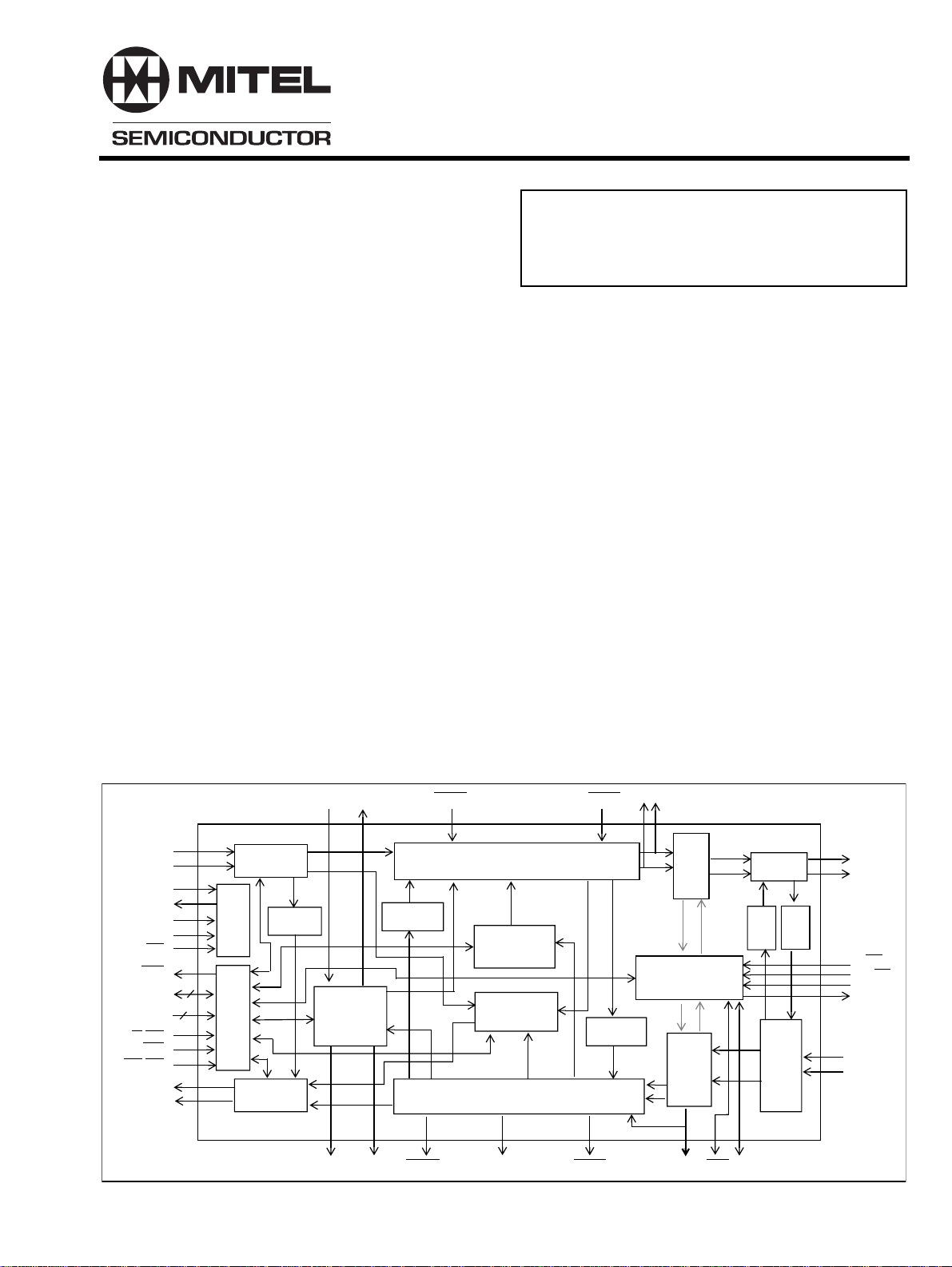
DSTi
CSTi
Tdi
Tdo
Tms
Tclk
Trst
IRQ
D7~D0
AC4
AC0
R/W/WR
CS
DS/RD
DSTo
CSTo
ST-BUS
Interface
ST Loop
IEEE
1149.1
Interface
Microprocessor
ST-BUS
Interface
RxDLCLK RxDL
TxDL TxDLCLK
Data Link,
HDLC0
HDLC1
Alarm Detection, 2 Frame Slip Buffer
Figure 1 - MT9076 Functional Block
TxMF
Transmit Framing, Error,
Test Signal Generation and Slip Buffer
PL Loop
National
Bit Buffer
CAS
Buffer
Receive Framing, Performance Monitoring,
TxAO TxB TxA
DG Loop
RxFP
Pulse
Generator
Jitter Attenuator
& Clock Control
Recovery
Clock,Data
Exclk
F0b C4bRxMF/TxFP LOS
Line
Driver
RM
Loop
MT
Rx Equalizer
& Data Slicer
Loop
TTIP
TRING
S/FR
BS/LS
OSC1
OSC2
RTIP
RRING
1
Page 2
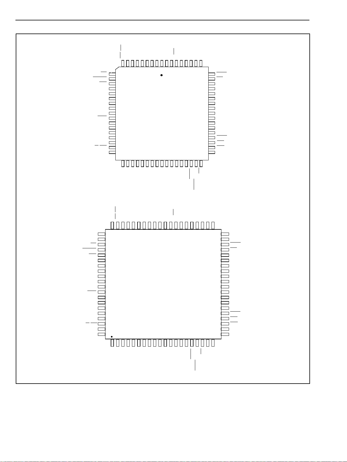
MT9076 Preliminary Information
FR/Exclki
DS/RD
DSTi
CSTi
DSTo
CSTo
VDD4
VSS4
OSC2
OSC1
VSS3
S/
VDD3
TxDLCK
TxDL
IC3
IC2
LOS
RESET
INT/
VDD5
R/
INT/
R/
NC
NC
CS
IRQ
D0
D1
D2
D3
VSS5
IC4
MOT
D4
D5
D6
D7
W/WR
AC0
NC
CS
RESET
IRQ
D0
D1
D2
D3
VSS5
IC4
MOT
VDD5
D4
D5
D6
D7
W/WR
AC0
8 6 4 2 68 66 64 62
10
12
14
16
AC3
CSTi
AC4
GNDARx
CSTo
68 PIN PLCC
RTIP
VDD1
RRING
VDDArx
VSS3
OSC1
OSC2
VSS4
VDD4
80 PIN LQFP
TXA
VSS1
VDD3
TXB
RxDCLK
FR/Exclki
TXDL
S/
18
20
22
24
26
28 30 32 34 36 38 40 42
AC1
AC2
NC
DS/RD
DSTo
DSTi
62
64
66
68
70
72
74
76
78
80
RxDL
TxMF
RxMF/TxFP
IC3
IC2
TCDLCK
60
58
56
54
52
50
48
46
44
LS
BS/
LOS
42444648505254565860
NC
NC
2018161412108642
TxAO
Trst
Tclk
Tms
Tdo
Tdi
GNDATX
TRING
TTIP
VDDATX
VDD2
VSS2
IC1
RxFP
F0b
C4b
Exclk
40
38
36
34
32
30
28
26
24
22
NC
NC
TxAO
Trst
Tclk
Tms
Tdo
Tdi
GNDATX
TRING
TTIP
VDDATX
VDD2
VSS2
IC1
RxFP
F0b
C4b
Exclk
NC
NC
AC1
AC3
AC2
AC4
RTIP
RRING
VDARx
GNDARx
VSS1
VDD1
TXA
TXB
RXDLCK
TxMF
RXDL
NC
BS/LS
RxMF/TxFP
NC
Figure 2 - Pin Connections
2
Page 3

Preliminary Information MT9076
Pin Description
Pin #
Name Description
PLCC LQFP
1 51 OSC1 Oscillator (3V Input). This pin is either connected via a 20.000 MHz crystal to OSC2
where a crystal is used, or is directly driven when a 20.000 MHz. oscillator is employed.
2 52 OSC2 Oscillator (3V Output). Connect a 20.0 MHz crystal between OSC1 and OSC2. Not
suitable for driving other devices.
353V
454V
5 55 CSTo Control ST-BUS (5V tolerant Output). CSTo carries serial streams for CAS and CCS
6 56 CSTi Control ST-BUS (5V tolerant Input). CSTi carries serial streams for CAS and CCS
7 57 DSTo Data ST-BUS (5V tolerant Output). A 2.048 Mbit/s serial stream which contains the
8 58 DSTi Data ST-BUS (5V tolerant Input). A 2.048 Mbit/s serial stream which contains the
959DS/RD Data/Read Strobe (5V tolerant Input).
SS4
DD4
Negative Power Supply . Digital ground.
Positive Power Supply . Digital supply (+3.3V ± 5%).
respectively a 2.048 Mbit/s ST-BUS status stream which contains the 30 receive
signaling nibbles (ABCDZZZZ or ZZZZABCD). The most significant nibbles of each ST-
BUS time slot are valid and the least significant nibbles of each ST-BUS time slot are
tristated when control bit MSN (page 01H, address 1AH, bit 1) is set to 1. If MSN=0, the
position of the valid and tristated nibbles are reversed.
respectively a 2.048 Mbit/s ST-BUS control stream which contains the 30 transmit
signaling nibbles (ABCDXXXX or XXXXABCD) when RPSIG=0. When RPSIG=1 this
pin has no function. The most significant nibbles of each ST-BUS time slot are valid and
the least significant nibbles of each ST-BUS time slot are ignored when control bit MSN
(page 01H, address 1AH, bit 1) is set to 1. If MSN=0, the position of the valid and
ignored nibbles is reversed.
24/30 PCM(T1/E1) or data channels received on the PCM 24/30 (T1/E1) line.
24/30 (T1/E1) PCM or data channels to be transmitted on the PCM 24/30 (T1/E1)
line.
In Motorola mode (DS), this input is the active low data strobe of the processor
interface. In Intel mode (RD), this input is the active low read strobe of the processor
interface.
10 63 CS Chip Select (5V tolerant Input). This active low input enables the non-multiplexed
parallel microprocessor interface of the MT9076. When CS is set to high, the
microprocessor interface is idle and all bus I/O pins will be in a high impedance state.
11 64 RESET RESET (5V tolerant Input). This active low input puts the MT9076 in a reset condition.
RESET should be set to high for normal operation. The MT9076 should be reset after
power-up. TheRESET pin must be held low for a minimum of 1µsec. to reset the device
properly .
12 65 IRQ Interrupt Request (5V tolerant Output). A low on this output pin indicates that an
interrupt request is presented. IRQ is an open drain output that should be connected to
VDD through a pull-up resistor. An active low CS signal is not required for this pin to
function.
13 -1666-69 D0 - D3 Data 0 to Data 3 (5V tolerant Three-state I/O). These signals combined with D4-D7
form the bidirectional data bus of the parallel processor interface (D0 is the least
significant bit).
17 70 VSS5 Negative Power Supply. Digital ground.
18 71 IC4 Internal Connection (3V Input). Tie to VSS (Ground) for normal operation.
3
Page 4

MT9076 Preliminary Information
Pin Description (continued)
Pin #
Name Description
PLCC LQFP
19 72 INT/MOT Intel/Motorola Mode Selection (5V tolerant Input). A high on this pin configures the
processor interface for the Intel parallel non-multiplexed bus type. A low configures the
processor interface for the Motorola parallel non-multiplexed type.
20 73 VDD5 Positive Power Supply. Digital supply (+3.3V ± 5%).
21 -2474-77 D4 - D7 Data 4 to Data 7 (5V tolerant Three-state I/O). These signals combined with D0-D3
form the bidirectional data bus of the parallel processor interface (D7 is the most
significant bit).
25 78 R/W/WR Read/Write/Write Strobe (5V tolerant Input). In Motorola mode (R/W), this input
controls the direction of the data bus D[0:7] during a microprocessor access. When R/W
is high, the parallel processor is reading data from the MT9076. When low, the parallel
processor is writing data to the MT9076. For Intel mode (WR), this active low write
strobe configures the data bus lines as output.
26 -3079,
31 6 GNDARx Receive Analog Ground. Analog ground for the LIU receiver.
32
33
34 9 VDDARx Receive Analog Power Supply. Analog supply for the LIU receiver (+3.3V ± 5%).
35 10 VDD1 Positive Power Supply. Digital supply (+3.3V ± 5%).
36 11 VSS1 Negative Power Supply. Digital ground.
37 12 TxA Transmit A (5V tolerant Output). When the internal LIU is disabled (digital framer
38 13 TxB Transmit B (5V tolerant Output). When the internal LIU is disabled and control bit
39 14 RxDLCLK Data Link Clock (5V tolerant Output). A gapped clock signal derived from the
AC0 - AC4 Address/Control 0 to 4 (5V tolerant Inputs). Address and control inputs for the
2-5
7
8
RTIP
RRING
non-multiplexed parallel processor interface. AC0 is the least significant input.
Receive TIP and RING (3V Input). Differential inputs for the receive line signal - must
be transformer coupled (See Figure 6). In digital framer mode these pins accept digital
3 volt signals from a physical layer device. They may accept a split phase unipolar
signal (RTIP and RRING employed) or an NRZ signal (RTIP only used).
only mode), if control bit NRZ=1, an NRZ output data is clocked out on pin TxA with the
rising edge of Exclk (TxB has no function when NRZ format is selected). If NRZ=0, pins
TxA and TxB are a complementary pair of signals that output digital dual-rail data
clocked out with the rising edge of Exclk.
NRZ=0, pins TxA and TxB are a complementary pair of signals that output digital dualrail data clocked out with the rising edge of Exclk.
extracted line clock, available for an external device to clock in RxDL data (at 4, 8, 12,
16 or 20 kHz) on the rising edge.
40 15 RxDL Receive Data Link (5V tolerant Output). A serial bit stream containing received line
data after zero code suppression. This data is clocked out with the rising edge of Exclk.
41 16 TxMF Transmit Multiframe Boundary (5V tolerant Input). An active low input used to set
the transmit multiframe boundary (CAS or CRC multiframe). The MT9076 will generate
its own multiframe if this pin is held high. This input is usually pulled high for most
applications.
4
Page 5

Preliminary Information MT9076
Pin Description (continued)
Pin #
Name Description
PLCC LQFP
42 17 RxMF/
TxFP
Receive Multiframe Boundary / Transmit Frame Boundary (5V tolerant Output). If
the control bit Tx8KEN (page 02H address 10H bit 2) is low, this negative output pulse
delimits the received multiframe boundary. The next frame output on the data stream
(DSTo) is basic frame zero on the T1 or PCM 30 link. In E1 mode this receive
multiframe signal can be related to either the receive CRC multiframe (page 01H,
address 17H, bit 6, MFSEL=1) or the receive signaling multiframe (MFSEL=0). If the
control bit Tx8KEN is set high, this positive output pulse delimits the frame boundary
(the first bit transmit in the frame) for the digital output stream on pins TXA and TXB.
43 18 BS/LS Bus/Line Syncronization Mode Selection (5V tolerant Input). If high, C4b and F0b
will be inputs; if low, C4b and F0b will be outputs.
44 22 Exclk 2.048 MHz in E1 mode or 1.544MHz in T1 mode, Extracted Clock (5V tolerant
Output). The clock extracted from the received signal and used internally to clock in
data received on RTIP and RRING.
45 23 C4b 4.096 MHz System Clock (5V tolerant Input/Output). C4b is the clock for the ST-BUS
sections and transmit serial PCM data of the MT9076. In the free-run (S/FR/Exclki=0) or
line synchronous mode (S/FR/Exclki=1 and BS/LS=0) this signal is an output, while in
bus synchronous mode (S/FR/Exclki=1 and BS/LS=1) this signal is an input clock.
46 24 F0b Frame Pulse (5V tolerant Input/Output). This is the ST-BUS frame synchronization
signal, which delimits the 32 channel frame of CSTi, CSTo, DSTi, DSTo and the
PCM30 link. In the free-run (S/FR/Exclki=0) or line synchronous mode (S/FR/Exclki=1
and BS/LS=0) this signal is an output, while in bus synchronous mode (S/FR/Exclki=1
and BS/LS=1) this signal is an input.
47 25 RxFP Receive Frame Pulse/Receive CCS Clock (5V tolerant Output). An 8kHz pulse
signal, which is low for one extracted clock period. This signal is synchronized to the
receive DS1 or PCM 30 basic frame boundary.
48 26 IC1 Internal Connection. Must be left open for normal operation.
49 27 V
50 28 V
SS2
DD2
51 29 VDD
525330
31
TTIP
TRING
54 32 GND
Negative Power Supply. Digital ground.
Positive Power Supply. Digital supply (+3.3V ± 5%).
Transmit Analog Power Supply. Analog supply for the LIU transmitter (+3.3V ±5%).
ATx
Transmit TIP and RING(Output). Differential outputs for the transmit line signal - must
be transformer coupled (See Figure 6).
Transmit Analog Ground . Analog ground for the LIU transmitter.
ATx
55 33 Tdi IEEE 1149.1a Test Data Input (3V Input). If not used, this pin should be pulled high.
56 34 Tdo IEEE 1149.1a Test Data Output (5V tolerant Output). If not used, this pin should be
left unconnected.
57 35 Tms IEEE 1149.1a Test Mode Selection (3V Input). If not used, this pin should be pulled
high.
58 36 Tclk IEEE 1149.1a Test Clock Signal (3V Input). If not used, this pin should be pulled high.
59 37 Trst IEEE 1149.1a Reset Signal (3V Input). If not used, this pin should be held low.
60 38 TxAO Transmit All Ones (Input). High - TTIP, TRING will transmit data normally. Low - TTIP,
TRING will transmit an all ones signal.
5
Page 6

MT9076 Preliminary Information
Pin Description (continued)
Pin #
Name Description
PLCC LQFP
61 43 LOS Loss of Signal or Synchronization (5V tolerant Output). When high, and LOS/LOF
(page 01H address 19H bit 0) is zero, this signal indicates that the receiv e portion of the
MT9076 is either not detecting an incoming signal (bit LLOS on page 03H address 16H
is one) or is detecting a loss of basic frame alignment condition (bit TSYNC (T1), SYNC
(E1) on page 03H address 10H is one). If LOS/LOF=1, a high on this pin indicates a
loss of signal condition.
62 44 IC2 Internal Connection (3V Input). Tie to VSS (Ground) for normal operation.
63 45 IC3 Internal Connection (3V Input). Tie to VSS (Ground) for normal operation.
64 46 TxDLCLK Transmit Data Link Clock (5V tolerant Output). A gapped clock signal derived from a
gated 2.048 Mbit/s clock for transmit data link at 4, 8, 12, 16 or 20 kHz. The transmit
data link data (TxDL) is clocked in on the rising edge of TxDLCLK. TxDLCLK can also
be used to clock DL data out of an external serial controller.
65 47 TxDL Transmit Data Link (5V tolerant Input). An input serial stream of transmit data link
data at 4, 8, 12, 16 or 20 kbit/s.
66 48 S/FR/
Exclki
67 49 VDD3 Positive Power Supply. Digital supply (+3.3V ± 5%).
68 50 VSS3 Negative Power Supply. Digital ground.
Synchronization/ Freerun / Extracted Clock (5V tolerant Input). If low, and the
internal LIU is enabled, the MT9076 is in free run mode. Pins 45 C4b and 46 F0b are
outputs generating sytem clocks. Slips will occur in the receive slip buffer as a result of
any deviation between the MT9076's internal PLL (which is free - running) and the
frequency of the incoming line data. If high, and the internal LIU is enabled, the MT9076
is in Bus or Line Synchronization mode depending on the BS/LS pin. If the internal LIU
is disabled, in digital framer mode, this pin (Exclki) tak es an input cloc k 1.544Mhz (T1) /
2.048Mhz (E1) that clocks in the received digital data on pins RXA and RXB with its
rising edge.
Device Overview
The MT9076 is a T1/E1/J1 single chip transceiver that incorporates an advanced framer, a long-haul LIU (Line
Interface Unit), a low jitter PLL (Phase Locked Loop) and 3 HDLCs (High-level Data Link Controller). The T1,
E1 and J1 operating modes are selectable under software control.
Standards Compliance
In T1 mode, the MT9076 meets or supports the latest recommendations including Telcordia GR-303-CORE,
AT&T PUB43801, TR-62411, ANSI T1.102, T1.403 and T1.408. In T1 ESF mode the CRC-6 calculation and
yellow alarm can be configured to meet the requirements of a J1 interface.
In E1 mode, the MT9076 meets or supports the latest ITU-T Recommendations for PCM 30 and ISDN primary
rate including G.703, G.704, G.706, G.732, G.775, G.796, G.823, G.964 (V5.1), G.965 (V5,2) and I.431. It also
meets or supports ETSI ETS 300 011, ETS 300 166, ETS 300 233, ETS 300 324 (V5.1) and ETS 300 347
(V5.2).
Microprocessor Port
The MT9076 registers are accessible via an 8-bit parallel Motorola or Intel non-multiplexed microprocessor
interface.
6
Page 7

Preliminary Information MT9076
LIU
The MT9076 LIU interfaces the digital framer functions to either the DS1 (T1 mode) or PCM 30 (E1 mode)
transformer-isolated four wire line.
In T1 mode, the LIU can pre-equalize the transmit signal to meet the T1.403 and T1.102 pulse templates after
attenuation by 0 - 655 feet of 22 AWG PIC cable, alternatively it can provide line build outs of 7.5dB, 15dB and
22.5dB. In T1 mode the receiver can recover signals attenuated by up to 43dB at 772kHz.
In E1 mode, the LIU transmits signals that meet the G.703 2.048 Mbit/s pulse template and the receiver can
recover signals attenuated by up to 43dB at 1024kHz.
Digitial Framer Only Mode
To accommodate some special applications, the MT9076 suppor ts a digital framer only mode that provides
direct access to the transmit and receive data in digital format, i.e. by-passing the analog LIU front-end. In
digital framer only mode, the MT9076 supports unipolar non-return to zero or bipolar return to zero data.
PLL and Slip Buffers
The MT9076 PLL attenuates jitter from 2.5 Hz with a roll-off of 20 dB/decade. The intrinsic jitter is less than
0.02 UI. The device can operate in one of three timing modes: System Bus Synchronous Mode, Line
Synchronous Mode, or Free-run Mode. In all three timing modes the low jitter output of the PLL provides timing
to the transmit side of the LIU.
In T1 mode, the receive and transmit paths both include two-frame slip buffers. The transmit slip buffer features
programmable delay and serves as a Jitter Attenuator (JA) FIFO and a rate converter between the ST-BUS and
the 1.544 Mbit/s T1 line rate.
In E1 mode, the receive path includes a two-frame slip buffer and the transmit path contains a 128 bit Jitter
Attenuator (JA) FIFO with programmable depth.
Interface to the System Backplane
On the system side the MT9076 framers can interface to a 2.048Mbit/s or 8.192Mbit/s ST-BUS backplane.
There is an asynchronous mode for Inverse MUX for ATM (IMA) applications, this enables the framer to
interface to a 1.544Mbit/s (T1) or 2.048Mbit/s (E1) serial bus with asynchronous transmit and receive timing.
Framing Modes
The MT9076 framers operate in termination mode or transparent mode. In the receive transparent mode, the
received line data is channelled to the DSTo pin with arbitrary frame alignment. In the transmit transparent
mode, no framing or signaling is imposed on the data transmitted from the DSTi pin onto the line.
In T1 mode, the framers operate in any of the following framing modes: D4, Extended Superframe (ESF) or
SLC-96.
In E1 mode, the framers run three framing algorithms: basic frame alignment, signaling multiframe alignment
and CRC-4 multiframe alignment. The Remote Alarm Indication (RAI) bit is automatically controlled by an
internal state machine.
7
Page 8

MT9076 Preliminary Information
Access to the Maintenance Channel
The T1 ESF Facility Data Link (FDL) bits can be accessed in the following three ways: Through the data link
pins TxDL, RxDL, RxDLC and TxDLC; through internal registers for Bit Oriented Messages; through an
embedded HDLC.
In E1 mode, the Sa bits (bits 4-8 of the non-frame alignment signal) can be accessed in four ways: Through
data link pins TxDL, RxDL, RxDLC and TxDLC, through single byte transmit and receive registers; through five
byte transmit and receive national bit buffers; through an embedded HDLC.
Robbed Bit Signaling/Channel Associated Signaling
Robbed bit signaling and channel associated signaling information can be accessed two ways: Via the
microport; via the CSTi and CSTo pins. Signaling information is frozen upon loss of multiframe alignment.
In T1 mode, the MT9076 supports AB and ABCD robbed bit signaling. Robbed bit signaling can be enabled on
a channel by channel basis.
In E1 mode the MT9076 supports Channel Associated Signaling (CAS) multiframing.
HDLCs
The MT9076 provides three embedded HDLCs with 128 byte deep transmit and receive FIFOs.
In T1 mode, the embedded HDLCs can be assigned to any channel and can operate at 56 kbit/s or 64 kbit/s. In
T1 ESF mode, HDLCO can be assigned to the 4 kbit/s FDL.
In E1 mode, the embedded HDLCs can be assigned to any timeslot and can operate at 64kbit/s. HDLCO can
be assigned to timeslot 0 Sa bits (bits 4-8 of the non-frame alignment signal) and can operate at 4,8,12,16 or
20kbit/s.
Performance Monitoring and Debugging
The MT9076 has a comprehensive suite of performance monitoring and debugging features. These include
error counters, loopbacks, deliberate error insertion and a 215 –1 QRS/PRBS generator/detector.
Interrupts
The MT9076 provides a comprehensive set of maskable interrupts. Interrupt sources consist of
synchronization status, alarm status, counter indication and overflow, timer status, slip indication, maintenance
functions and receive signaling bit changes.
8
Page 9

Preliminary Information MT9076
MT9076 Detailed Feature List
Standards Compliance and Support
T1/J1 Mode E1 Mode
ANSI:
T1.102,T1.231, T1.403, T1.408
AT&T:
TR 62411, PUB43801
Telcordia:
GR-303-CORE
TTC:
JT-G703, JT-G704, JT-G706
Line Interface Unit (LIU)
• T1 and E1 modes use the same 1:2.4 transmit and receive transformers
• Internal register allows termination imepedance to be changed under software control.
• Programmable pulse shapes and pulse amplitudes
• Automatic or manual receiver equalization
• Receive signal peak amplitude is reported with 8-bit resolution
• Output pin to indicate Loss Of Signal/ Loss Of Frame synchronization
• LIU output is disabled at power-up until enabled by software
• Input pin to force transmission of AIS
ETSI:
ETS 300 011, ETS 300 166, ETS 300 233,
ETS 300 324, ETS 300 347
ITU:
G.703, G.704, G.706, G.732 G.775,
G.796, G.823, I.431, G.964, G.965
T1/J1 Mode E1 Mode
• Reliably recovers signals with cable
attenuation up to 43dB @ 772 kHz
• Transmit pulse meets T1.403 and T1.102
pulse templates
• Indicates analog Los Of Signal if the received
signal is more than 20 dB or 40dB below
nominal for more than 1ms
• Receiver tolerates jitter as required by AT&T
TR62411
• Transmit Pre-equalization and Line Build Out
options:
0-133 feet
133-266 feet
266-399 feet
399-533 feet
533-655 feet
-7.5dB
-15dB
-22.5dB
• Reliably recovers signals with cable
attenuation up to 43 dB @ 1024 kHz
• Transmit pulse meets G.703 pulse template
• Indicates analog Los Of Signal if the received
signal is more than 20dB or 40dB below
nominal for more than 1ms
• Receiver tolerates jitter as required by ETSI
ETS 300 011
9
Page 10

MT9076 Preliminary Information
Digital Framer Mode
• The LIU can be disabled and bypassed to allow the MT9076 to be used as a digital framer
• Single phase NRZ or two phase NRZ modes are software selectable
• Line coding is software selectable
Phase Lock Loop
• Locks to a 4.096 MHz input clock, or to the 1.544MHz / 2.048MHz extracted clock
• IMA mode locks to 1,544MHz or 2,048MHz external clock
• Attenuates jitter from less than 2.5 Hz with a roll off of 20 dB/decade
• Attenuates jitter in the transmit or receive direction
• Intrinsic jitter less than 0.02 UI
• Meets the jitter characteristics as specified in AT&T TR62411
• Meets the jitter characteristics as specified in ETS 300 011
• Can be operated in Free-run, Line Synchronous or System Bus Synchronous modes
Access and Control
• MT9076 registers can be accessed via an 8-bit non-multiplexed parallel microprocessor port
• The parallel port can be configured for Motorola or Intel style control signals
Backplane Interfaces
• 2.048Mbit/s or 8.192Mbit/s ST-BUS
• IMA mode, 1.544Mbit/s (T1) or 2.048Mbit/s (E1) serial bus with asynchronous transmit and receive
timing for Inverse MUX for ATM (IMA) applications. Slip buffers are bypassed and signaling is disabled.
• CSTo/CSTi pins can be used to access the receive/transmit signaling data
• RxDL pin can be used to access the entire B8ZS/HDB3 decoded receive stream including framing bits
• TxDL pin can be used to transmit data on the FDL (T1) or the Sa bits (E1)
T1/J1 Mode E1 Mode
• PCM-24 channels 1-24 are mapped to STBUS channels 0-23 respectively
• The framing-bit is mapped to ST-BUS
channel 31
• PCM-30 timeslots 0-31 are mapped to STBUS channels 0-31 respectively
10
Page 11

Preliminary Information MT9076
Data Link
T1/J1 Mode E1 Mode
• Three methods are provided to access the
datalink:
1. TxDL and RxDL pins support transmit and
receive datalinks
2. Bit Oriented Messages are supported via
internal registers
3. An internal HDLC can be assigned to transmit/
receive over the FDL in ESF mode
Access and Monitoring for National (Sa) Bits (E1 mode only)
• In addition to the datalink functions, the Sa bits can be accessed using:
• Single byte register
• Five byte transmit and receive national bit buffers
• A maskable interrupt is generated on the change of state of any Sa bit
Three Embedded Floating HDLCs (HDLC0, HDLC1, HDLC2)
• Successive writes/reads can be made to the transmit/receive FIFOs at 160 ns or 80ns intervals
• Flag generation and Frame Check Sequence (FCS) generation and detection, zero insertion and
deletion
• Continuous flags, or continuous 1s are transmitted between frames
• Transmit frame-abor t
• Transmit end-of-packet after a programmable number of bytes (up to 65,536 bytes)
• Invalid frame handling:
• Frames yielding an incorrect FCS are tagged as bad packets
• Frames with fewer than 25 bits are ignored
• Frames with fewer than 32 bits between flags are tagged as bad packets
• Frames interrupted by a Frame-Abort sequence remain in the FIFO and an interrupt is generated
• Access is provided to the receive FCS
• FCS generation can be inhibited for terminal adaptation
• Recognizes single byte, dual byte and all call addresses
• Independent, 16-128 byte deep transmit and receive FIFOs
• Receive FIFO maskable interrupts for near full (programmable levels) and overflow conditions
• Transmit FIFO maskable interrupts for nearly empty (programmable levels) and underflow conditions
• Maskable interrupts for transmit end-of-packet and receive end-of-packet
• Maskable interrupts for receive bad-frame (includes frame abort)
• Transmit-to-receive and receive-to-transmit loopbacks are provided
• Transmit and receive bit rates and enables are independent
• Frame aborts can be sent under software control and they are automatically transmitted in the event of
a transmit FIFO underrun
• Two methods are provided to access the
datalink:
1. TxDL and RxDL pins support transmit and
receive datalinks over the Sa4~Sa8 bits
2. An internal HDLC can be assigned to transmit/
receive data via the Sa4~Sa8 bits
• In transparent mode, if the Sa4 bit is used for
an intermediate datalink, the CRC-4
remainder can be updated to reflect changes
to the Sa4 bit
11
Page 12

MT9076 Preliminary Information
T1/J1 Mode E1 Mode
HDLC0
• Assignable to the ESF Facility Data Link or
any channel
• Operates at 4 kbps, 56 kbps or 64 kbps
HDLC1, HDLC2
• Assignable to any channel
• Operates at 56 kbps or 64 kbps
Slip Buffers
T1/J1 Mode E1 Mode
Transmit Slip Buffer
• Two-frame slip buffer capable of performing a
controlled slip
• Intended for rate conversion and jitter
attenuation in the transmit direction
• Programmable delay • Indication of slip direction
• Transmit slips are independent of receive
slips
• Indication of slip direction
HDLC0
• Assigned to timeslot-0, bits Sa4~Sa8 or any
other timeslot
• Operates at 4, 8, 12, 16 or 20 kbps
depending on which Sa bits are selected for
HDLC0 use
HDLC1, HDLC
• Assigned to any timeslot except timeslot-0
• Operates at 64 kbps
Receive Slip Buffer
• Two-frame slip buffer capable of performing a
controlled slip
• Wander tolerance of 208 UI peak-to-peak
Receive Slip Buffer
• Two-frame slip buffer capable of performing a
controlled slip
• Wander tolerance of 142 UI (92 µs) peak
• Indication of slip direction
Jitter Attenuator FIFO
• A jitter attenuator FIFO is available on the transmit side in E1 mode and in IMA mode. The depth of the
JA FIFO can be configured to be from16 bits deep to 128 bits deep in 16 bit increments
Inverse Mux for ATM (IMA) Mode
T1/J1 Mode E1 Mode
• Transmit and receive datastreams are
independently timed
• The transmit clock synchronizes to a
1,544MHz clock
• Transmit and receive slip buffers are
bypassed
• Transmit and receive datastreams are
independently timed
• Receive slip buffer is bypassed
• CAS and HDLCs are disabled
• Robbed bit signaling and HDLCs are disabled
12
Page 13

Preliminary Information MT9076
Framing Algorithm
T1/J1 Mode E1 Mode
• Synchronizes with D4 or ESF protocols
• Supports SLC-96 framing
• Framing circuit is off-line
• Transparent transmit and receive modes
• In D4 mode the Fs bits can optionally be
cross checked with the Ft bits
• The start of the ESF multiframe can be
determined by the following methods:
• Free-run
• Software reset
• Synchronized to the incoming multiframe
• An automatic reframe is initiated if the
framing bit error density exceeds the
programmed threshold
• In transparent mode, no reframing is forced
by the device
• Software can force a reframe at any time
• In ESF mode the CRC-6 bits can be
optionally confirmed before forcing a new
frame alignment
• During a reframe the signaling bits are frozen
and error counting for Ft, Fs, ESF framing
pattern and CRC-6 bits is suspended
• If J1 CRC-6 is selected the Fs bits are
included in the CRC-6 calculation
• J1 CRC-6 and J1 Yellow Alarm can be
independently selected
• Supports robbed bit signaling
• MT9076 contains 3 distinct and independent
framing algorithms
1. Basic frame alignment
2. Signaling multiframe alignment
3. CRC-4 multiframe alignment
• Transparent transmit and receive modes
• Automatic interworking between interfaces
with and without CRC-4 processing
capabilities is supported
• An automatic reframe is forced if 3
consecutive frame alignment patterns or
three consecutive non-frame alignment bits
are received in error
• In transparent mode, no reframing is forced
by the device
• Software can force a reframe at any time
• Software can force a multiframe reframe at
any time
• E-bits can optionally be set to zero until CRC
synchronization is achieved
• Optional automatic RAI
• Supports CAS multiframing
• Optional automatic Y-bit to indicate CAS
multiframe alignment
Line Coding
T1/J1 Mode E1 Mode
• B8ZS or AMI line coding
• Pulse density enforcement
• Forced ones insertion
• HDB3 or AMI line coding
13
Page 14

MT9076 Preliminary Information
Channel Associated Signaling
• ABCD or AB bits can be automatically inserted and extracted
• Transmit ABCD or AB bits can be passed via the micropor t or via the CSTi pin
• Receive ABCD or AB bits are accessible via the microport or via the CSTo pin
• Most significant or least significant CSTi/CSTo nibbles can be selected to carr y signaling bits
• Unused nibble positions in the CSTi/CSTo bandwidth are tri-stated
• An interrupt is provided in the event of changes in any of the signaling bits
• Receive signaling bits are frozen if signaling multiframe alignment is lost
T1/J1 Mode E1 Mode
• Signaling bits can be debounced by 6 ms • Signaling bits can be debounced by14 ms
Alarms
T1/J1 Mode E1 Mode
D4 Yellow Alarm, two types
1. Bit position 2 is zero for virtually every DS0
over 48ms
2. Two consecutive ones in the S-bit position of
the twelfth frame
ESF Yellow Alarm, two types
1. Reception of 0000000011111111 in seven
or more codewords out of ten (T1)
2. Reception of 1111111111111111 in seven
or more codewords out of ten (J1)
Alarm Indication Signal (AIS)
• Declared if fewer than six zeros are detected
during a 3 ms interval
Loss Of Signal (LOS
• Analog Loss Of Signal is declared if the
received signal is more than 20 dB or 40 dB
below nominal for at least 1 ms
• Digital Loss Of Signal is declared if 192 or 32
consecutive zeros are received
• Output pin indicates LOS and/or loss of
frame alignment
)
Remote Alarm Indication (RAI)
• Bit 3 of the receive NFAS
Alarm Indication Signal (AIS
• Unframed all ones signal for at least a double
frame or two double frames
)
Timeslot 16 Alarm Indication Signal
• All ones signal in timeslot 16
Loss Of Signal (LOS)
• Analog Loss Of Signal is declared if the
received signal is more than 20 dB or 40 dB
below nominal for at least 1 ms
• Digital Loss Of Signal is declared if 192 or 32
consecutive zeros are received
• Output pin indicates LOS and/or loss of
frame alignment
Remote Signaling Multiframe Alarm
• Y-bit of the multiframe alignment signal
14
Page 15

Preliminary Information MT9076
Maskable Interrupts
T1/J1 Mode E1 Mode HDLC Interrupts
• Change of state of terminal
synchronization
• Change of state of multiframe
synchronization
• Change of received bit
oriented message
• Change of state of reception
of AIS
• Change of state of reception
of LOS
• Reception of a severely
errored frame
• Transmit slip
• Receive slip
• Receive framing bit error
• Receive CRC-6 error
• Receive yellow alarm
• Change of receive frame
alignment
• Receive line code violation
• Receive PRBS error
• Pulse density violation
• Framing bit error counter
overflow
• CRC-6 error counter overflow
• Out of frame alignment
counter overflow
• Change of frame alignment
counter overflow
• Line code violation counter
overflow
• PRBS error counter overflow
• PRBS multiframe counter
overflow
• Multiframes out of alignment
counter overflow
• Loop code detected
• One second timer
• Five second timer
• Receive new bit oriented
message (debounced)
• Signaling (AB or ABCD) bit
change
• Change of state of basic
frame alignment
• Change of state of multiframe
synchronization
• Change of state of CRC-4
multiframe synchronization
• Change of state of reception
of AIS
• Change of state of reception
of LOS
• Reception of consecutively
errored FASs
• Receive remote signaling
multiframe alarm
• Receive slip
• Receive FAS error
• Receive CRC-4 error
• Receive E-bit
• Receive AIS in timeslot 16
• Line code violation
• Receive PRBS error
• Receive auxiliary pattern
• Receive RAI
• FAS error counter overflow
• CRC-4 error counter overflow
• Out of frame alignment
counter overflow
• Receive E-bit counter
overflow
• Line code violation counter
overflow
• PRBS error counter overflow
• PRBS multiframe counter
overflow
• Change of state of any Sa bit
or Sa nibble
• Jitter attenuator within 4 bits
of overflow/underflow
• One second timer
• Two second timer
• Signaling (CAS) bit change
• Go ahead pattern received
• End of packet received
• End of packet transmitted
• End of packet read from
receive FIFO
• Transmit FIFO low
• Frame abort received
• Transmit FIFO underr un
• Receive FIFO full
• Receive FIFO overflow
15
Page 16

MT9076 Preliminary Information
Error Counters
• All counters can be preset or cleared under software control
• Maskable occurrence interrupt
• Maskable overflow interrupt
• Counters can be latched on one second intervals
T1/J1 Mode E1 Mode
• PRBS Error Counter (16-bit)
• CRC Multiframe Counter (16-bit)
• Framing Bit Error Counter (8-bit)
• Out of Frame Alignment Counter (4-bit)
• Change of Frame Alignment Counter (4-bit)
• Multiframes Out of Sync Counter (8-bit)
• Line Code Violation / Excessive Zeros
Counter (16-bit)
• CRC-6 Error Counter (16-bit)
Error Insertion
T1/J1 Mode E1 Mode
• Bipolar Violations
• CRC-6 Errors
• Ft Errors
• Fs Errors
• Payload Errors
• Loss of Signal Error
Loopbacks
• Errored FAS Counter (8-bit)
• E-bit Counter (10-bit)
• Line Code Violation / Excessive Zeros
Counter (16-bit)
• CRC-4 Error Counter (16-bit)
• PRBS Error Counter (8-bit)
• CRC Multiframe Counter (8-bit)
• Bipolar Violations
• CRC-4 Errors
• FAS Errors
• NFAS Errors
• Payload Errors
• Loss of Signal Error
• Digital loopback
• Remote loopback
• ST-BUS loopback
• Payload loopback
• Metallic loopback
• Local timeslot loopback
• Remote timeslot loopback
Per Timeslot Control
The following features can be controlled on a per timeslot basis:
• Clear Channel Capability (only used in T1/J1)
• Choice of sourcing transmit signaling bits from microport or CSTi pin
• Remote timeslot loopback
• Local timeslot loopback
• PRBS insertion and reception
• Digital milliwatt pattern insertion
• Per channel inversion
• Transmit message mode
16
Page 17

MT9076
1.0 MT9076 Line Interface Unit (LIU)..................................................................................17
1.1 Receiver .................................................................................................................................................17
1.2 Transmitter .............................................................................................................................................18
1.3 20 Mhz Clock..........................................................................................................................................21
1.4 Phase Lock Loop (PLL)..........................................................................................................................22
2.0 Clock Jitter Attenuation Modes....................................................................................23
2.1 Jitter Attenuator FIFO.............................................................................................................................24
2.2 IMA Mode...............................................................................................................................................24
2.2.1 T1 Mode ......................................................................................................................................... 24
2.2.2 E1 Mode......................................................................................................................................... 24
3.0 The Digital Interface ......................................................................................................24
3.1 T1 Digital Interface .................................................................................................................................24
3.2 Frame and Superframe Structure in T1 mode........................................................................................25
3.2.1 Multiframing.................................................................................................................................... 25
3.3 E1 Digital Interface.................................................................................................................................27
3.3.1 Basic Frame Alignment .................................................................................................................. 28
3.3.2 CRC-4 Multiframing in E1 mode..................................................................................................... 29
3.3.3 CAS Signaling Multiframing in E1 mode......................................................................................... 30
4.0 MT9076 Access and Control.........................................................................................30
4.1 The Control Port Interface......................................................................................................................30
4.2 Control and Status Register Access.......................................................................................................31
4.3 Identification Code..................................................................................................................................31
4.4 ST-BUS Streams....................................................................................................................................31
5.0 Reset Operation (Initialization).....................................................................................32
6.0 Transmit Data All Ones (TxAO) Operation ..................................................................33
7.0 Data Link Operation ......................................................................................................33
7.1 Data Link Operation in E1 mode ............................................................................................................33
7.2 Data Link Operation in T1 mode ............................................................................................................33
7.2.1 External Data Link.......................................................................................................................... 35
7.2.2 Bit - Oriented Messaging................................................................................................................ 35
8.0 Floating HDLC Channels ..............................................................................................35
8.1 Channel Assignment ..............................................................................................................................35
8.2 HDLC Description...................................................................................................................................36
8.2.1 HDLC Frame structure ................................................................................................................... 36
8.2.2 Data Transparency (Zero Insertion/Deletion)................................................................................. 36
8.2.3 Invalid Frames................................................................................................................................ 36
8.2.4 Frame Abort.................................................................................................................................... 37
xvii
Page 18

MT9076
8.2.5 Interframe Time Fill and Link Channel States ................................................................................ 37
8.2.6 Go-Ahead....................................................................................................................................... 37
8.3 HDLC Functional Description.................................................................................................................37
8.3.1 HDLC Transmitter........................................................................................................................... 37
8.3.2 HDLC Receiver............................................................................................................................... 38
9.0 Slip Buffers .................................................................................................................... 40
9.1 Slip Buffer in T1 Mode............................................................................................................................40
9.2 Slip Buffer in E1 mode............................................................................................................................42
10.0 Framing Algorithm ........................................................................................................ 43
10.1 Frame Alignment in T1 Mode.................................................................................................................43
10.2 Frame Alignment in E1 mode.................................................................................................................44
10.2.1 Notes for Synchronization State Diagram (Figure 16).................................................................... 46
10.3 Reframe..................................................................................................................................................46
10.3.1 E1 Mode........................................................................................................................................ 46
10.3.2 T1 Mode ......................................................................................................................................... 46
11.0 MT9076 Channel Signaling........................................................................................... 46
11.1 Channel Signaling in T1 Mode...............................................................................................................46
11.2 Channel Signaling in E1 Mode...............................................................................................................47
12.0 Loopbacks .....................................................................................................................48
13.0 Performance Monitoring............................................................................................... 49
13.1 Error Counters........................................................................................................................................49
13.2 T1 Counters............................................................................................................................................49
13.2.1 Framing Bit Error Counter (FC7-0)................................................................................................. 49
13.2.2 Out Of Frame / Change Of Frame Alignment Counter (OOF3-0/COFA3-0) .................................. 49
13.2.3 Multiframes out of Sync Counter (MFOOF7-MFOOF0).................................................................. 50
13.2.4 CRC-6 Error Counter (CC15-0)...................................................................................................... 50
13.2.5 Line Code Violation Error Counter (LCV15-LCV0)......................................................................... 50
13.2.6 PRBS Error Counter (PS7-0).......................................................................................................... 50
13.2.7 CRC Multiframe Counter for PRBS (PSM7-0)................................................................................ 50
13.3 E1 Counters ...........................................................................................................................................50
13.4 Errored FAS Counter (EFAS7-EFAS0)..................................................................................................50
13.5 E-bit Counter (EC15-0)...........................................................................................................................51
13.6 Line Code Violation Error Counter (LCV15-LCV0).................................................................................51
13.7 CRC-4 Error Counter (CC15-0)..............................................................................................................51
13.8 PRBS Error Counter (PS7-0) .................................................................................................................51
13.9 CRC Multiframe Counter for PRBS (PSM7-0)........................................................................................51
xviii
Page 19

MT9076
14.0 Error Insertion................................................................................................................52
15.0 Per Time Slot Control Words........................................................................................52
15.1 Clear Channel Capability........................................................................................................................52
15.2 Microport signaling .................................................................................................................................52
15.3 Per Time Slot Looping............................................................................................................................52
15.4 PRBS Testing.........................................................................................................................................53
15.5 Digital Milliwatt........................................................................................................................................53
15.6 Per Channel Inversion............................................................................................................................53
15.7 Transmit Message..................................................................................................................................54
16.0 Alarms ............................................................................................................................54
16.1 Automatic Alarms ...................................................................................................................................54
17.0 Detected Events.............................................................................................................55
17.1 T1 mode .................................................................................................................................................55
17.1.1 Severely Errored Frame Event....................................................................................................... 55
17.1.2 Loop Code Detect........................................................................................................................... 55
17.1.3 Pulse Density Violation Detect ....................................................................................................... 55
17.1.4 Timer Outputs................................................................................................................................. 55
17.2 E1 mode.................................................................................................................................................55
17.2.1 Consecutive Frame Alignment Patterns (CONFAP)....................................................................... 55
17.2.2 Receive Frame Alignment Signals ................................................................................................. 55
17.2.3 Receive Non Frame Alignment Signal............................................................................................ 55
17.2.4 Receive Multiframe Alignment Signals........................................................................................... 55
18.0 Interrupts........................................................................................................................55
18.1 Interrupts on T1 Mode............................................................................................................................56
18.2 Interrupts on E1 Mode............................................................................................................................56
19.0 Digital Framer Mode......................................................................................................57
19.1 T1 Mode .................................................................................................................................................57
19.1.1 E1 mode......................................................................................................................................... 57
20.0 Control and Status Registers.......................................................................................58
20.1 T1 Mode .................................................................................................................................................58
20.1.1 Master Control 1 (Page 01H) (T1).................................................................................................. 58
20.1.2 Master Control 2 (Page 02H) (T1).................................................................................................. 69
20.1.3 Master Status 1 (Page03H) (T1) .................................................................................................... 75
20.1.4 Master Status 2 (Page04H) (T1).................................................................................................... 80
20.1.5 Per Channel Transmit signaling (Pages 5 and 6) (T1) 88
20.2 Per Time Slot Control Words (Pages 7 and 8) (T1) ...............................................................................90
20.2.1 Per Channel Receive signaling (T1 and E1 mode) (Pages 9 and 0AH)......................................... 91
20.3 E1 Mode.................................................................................................................................................92
xix
Page 20

MT9076
20.3.1 Master Control 1 (Page 01H) (E1).................................................................................................. 92
20.4 Master Control 2 (Page-2)....................................................................................................................103
20.4.1 Master Control 2 (Page 02H) (E1)................................................................................................ 103
20.5 Master Status 1 (Page03H) (E1)..........................................................................................................109
20.6 Master Status 1 (Page03H) (E1)..........................................................................................................110
21.0 Master Status 2 (Page-4)............................................................................................117
21.1 Master Status 2 (Page 04H) (E1).........................................................................................................117
21.2 Per Channel Transmit signaling (Pages 5 and 6) (E1)........................................................................124
21.3 Per Time Slot Control Words (Pages 7 and 8) (E1).............................................................................125
21.4 Per Channel Receive signaling (Pages 9 and 0AH) (E1).....................................................................126
22.0 HDLC Control and Status (Page B for HDLC0, Page C for HDLC1 and Page D for
HDLC2) .........................................................................................................................127
23.0 Transmit National Bit Buffer (Page 0EH)...................................................................137
24.0 Receive National Bit Buffer (Page 0FH).....................................................................137
25.0 AC/DC Electrical Characteristics............................................................................... 138
xx
Page 21

Preliminary Information MT9076
1.0 MT9076 Line Interface Unit (LIU)
1.1 Receiver
The receiver portion of the MT9076 LIU consists of an input signal peak detector, an optional equalizer with
separate high pass sections, a smoothing filter, data and clock slicers and a clock extractor. Receive
equalization gain can be set manually (i.e., software) or it can be determined automatically by peak detectors.
The output of the receive equalizer is conditioned by a smoothing filter and is passed on to the clock and data
slicer. The clock slicer output signal drives a phase locked loop, which generates an extracted clock (Exclk).
This extracted clock is used to sample the output of the data comparator.
In T1 mode, the receiver portion of the LIU can recover clock and data from the line signal for loop lengths of 0
- 6000 ft. and tolerate jitter to the maximum specified by AT&T TR 62411(Figure 3).
The LOS output pin function is selectable to indicate any combination of loss of signal and/or loss of basic
frame synchronization condition.
The LLOS (Loss of Signal) status bit indicates when the receive signal level is lower than the analog threshold
for at least 1 millisecond, or when the number of consecutiv e received zeros exceeds the digital loss threshold.
In E1 mode, the analog threshold is either of -20 dB or -40 dB. The digital loss threshold is either 32 or 192.
In T1 mode, the receive LIU circuit requires a terminating resistor of 17.4Ω across the device side of the
receive 2.4:1 transformer.
In E1 mode, the receive LIU circuit requires a terminating resistor of either 20.8Ω or 13Ω across the device side
of the receive 2.4:1 transformer.
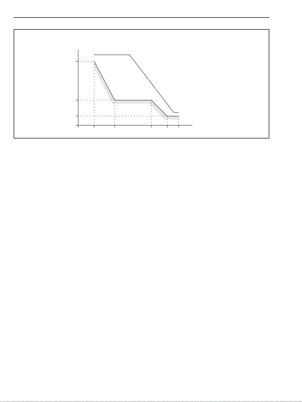
The jitter tolerance of the clock extractor circuit exceeds the requirements of TR 62411 in T1 mode (see Figure
3) and G.823 in E1 mode (see Figure 4).
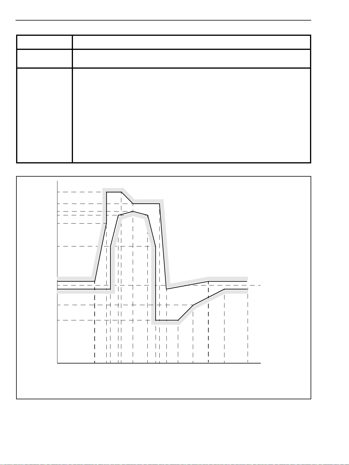
Peak to Peak
Jitter Amplitude
(log scale)
138UI
100UI
28UI
10UI
1.0UI
0.4UI
1.0Hz 10Hz 1.0kHz 10kHz 100kHz
0.1Hz 100Hz
4.9Hz
Jitter Frequency
(log scale)
Figure 3 - Input Jitter Tolerance as Recommended by TR-62411 (T1)
17
Page 22
MT9076 Preliminary Information
Peak to Peak
Jitter Amplitude
(log scale)
18UI
MT9076
Tolerance
1.5UI
0.2UI
1.667Hz 20Hz 2.4kHz 18kHz 100kHz
Jitter Frequency
(log scale)
Figure 4 - Input Jitter Tolerance as Recommended by G.823 and ETSI 300 011 (E1)
1.2 Transmitter
The transmit portion of the MT9076 LIU consists of a high speed digital-to-analog converter and
complementary line drivers.
When a pulse is to be transmitted, a sequence of digital values (dependent on transmit equalization) are read
out of a ROM by a high speed clock. These values drive the digital-to-analog converter to produce an analog
signal, which is passed to the complementary line drivers.
The complementary line drivers are designed to drive a 1:2.4 step-up transformer in T1 mode (see Figure 4 for
T1 mode) and either a 1:2 or 1:2.4 step-up transformer in E1 mode (see Figure 5 for E1 mode). A 0.47uF
capacitor is required between the TTIP and the transmit transformer. Resistors RT (as shown in Figure 4) are
for termination for transmit return loss. The values of RT may be optimized for T1 mode, E1 120Ω lines, E1 75Ω
lines or set at a compromise value to serve multiple applications. Program the Tx LIU Control Word (page 02H,
address 11H) to adjust the pulse amplitude accordingly.
Alternatively, the pulse level and shape may be discretely programmed by writing to the Custom Pulse Level
registers (page 2, addresses 1CH to 1FH) and setting the Custom Transmit Pulse bit high (bit 3 of the Tx LIU
Control Word). In this case the output of each of the registers directly drives the D/A converter going to the line
driver. Tables 1 and 2 show recommended transmit pulse amplitude settings.
In T1 mode, the template for the transmitted pulse (the DSX-1 template) is shown in Figure 8. The nominal
peak voltage of a mark is 3 volts. The ratio of the amplitude of the transmit pulses generated by TTIP and
TRING lie between 0.95 and 1.05.
In E1 mode, the template for the transmitted pulse, as specified in G.703, is shown in Figure 8. The nominal
peak voltage of a mark is 3 volts for 120 Ω twisted pair applications and 2.37 volts for 75 Ω coax applications.
The ratio of the amplitude of the transmit pulses generated by TTIP and TRING lie between 0.95 and 1.05.
18
Page 23
Preliminary Information MT9076
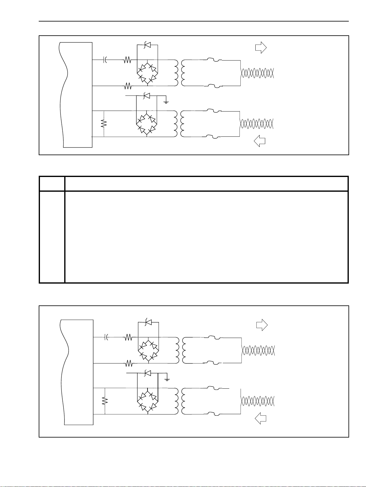
TTIP
TRING
RTIP
RRING
0.47uF
+3.3 V
17.36 Ω
R
T
R
T
1:2.4
1:2.4
Fuse
Tx
Fuse
RT: 2.4 Ω
Fuse
Fuse
Rx
Figure 5 - Analog Line Interface (T1)
Name Functional Description
TXL2-0 Transmit Line Build Out 2 - 0. Setting these bits shapes the transmit pulse as detailed in the table
below:
TXL2 TXL1 TXL0 Line Build Out
0 0 0 0 to 133 feet/ 0 dB
0 0 1 133 to 266 feet
0 1 0 266 to 399 feet
0 1 1 399 to 533 feet
1 0 0 533 to 655 feet
1 0 1 -7.5 dB
1 1 0 -15 dB
1 1 1 -22.5 dB
After reset these bits are zero.
TTIP
TRING
RTIP
RRING
0.47uF
20.83 Ω
RT
+3.3V
Table 1 - Transmit Line Build Out (T1)
1:2.4 (WR=0)
1:2 (WR=1)
RT
1:2.4
Fuse
Fuse
Fuse
Fuse
Figure 6 - Analog Line Interface (E1)
Tx
RT: Termination resistor. Please check
Table 2 for specific
resistor values.
Rx
19
Page 24
MT9076 Preliminary Information
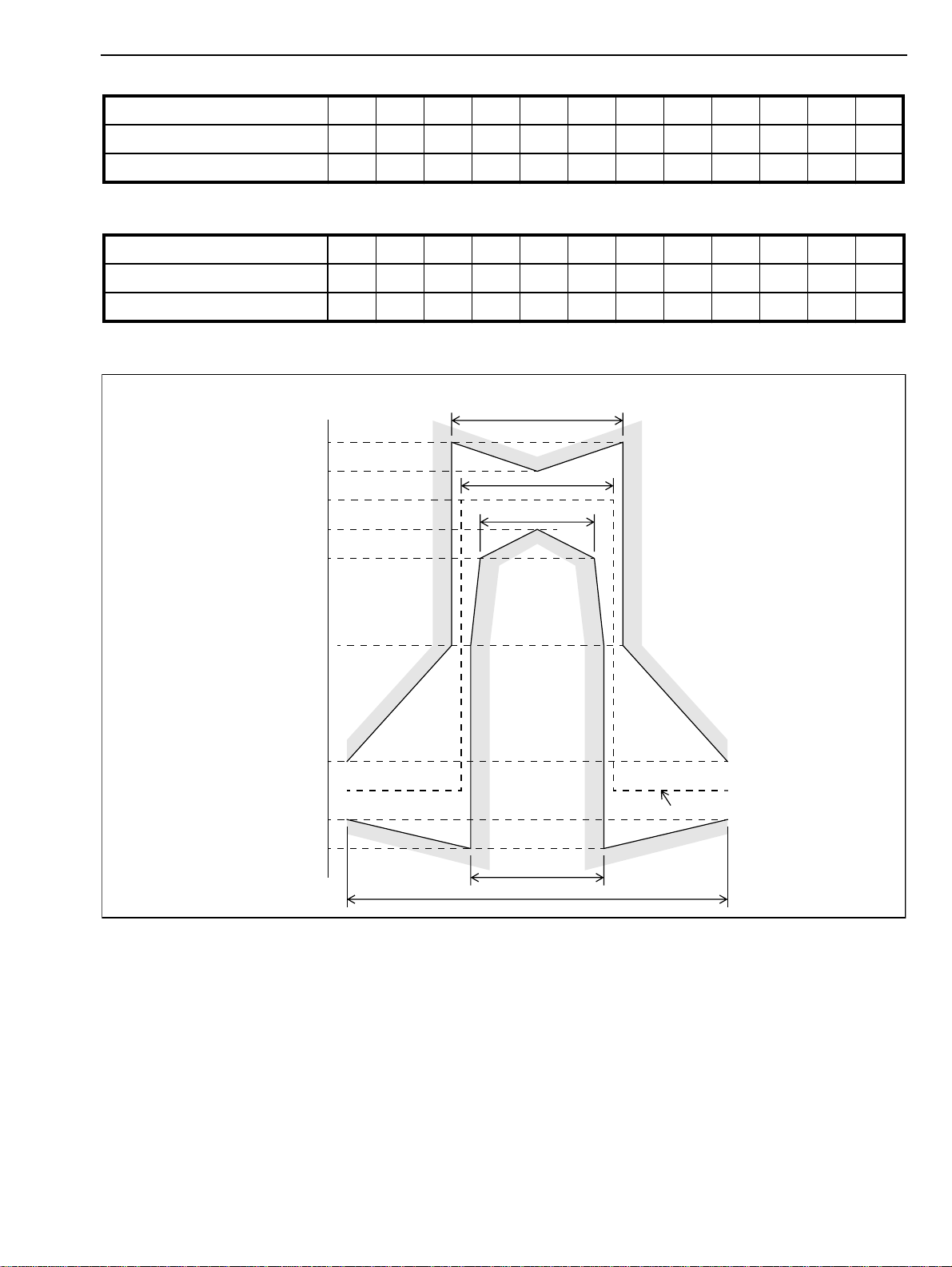
Name Functional Description
WR Winding Ratio. Set this pin low if a 1:2.4 transformer is used on the transmit side. Set this
pin high if a 1:2 transformer is used.
TX2-0 Transmit pulse amplitude. Select the TX2 –TX0 bits according to the line type, value of
termination resistors (RT), and transformer turns ratio used
TX2 TX1 TX0 Line Impedance(Ω) RT (Ω) Transformer Ratio
WR=0 WR=1 WR=0 WR=1
0 0 0 120 0 0 1:2.4 1:2
0 0 1 120 0 0 1:1 1:1
0 1 0 120 10.4 15 1:2.4 1:2
0 1 1 120 / 75 8.4 12.1 1:2.4 1:2
1 0 0 75 0 0 1:2.4 1:2
1 0 1 75 0 0 1:1 1:1
1 1 1 75 6.5 9.1 1:2.4 1:2
1 1 1 75 / 120 8.4 12.1 1:2.4 1:2
After reset these bits are zero.
Table 2 - Transmit Pulse Amplitude (E1)
1.20
1.05
0.95
0.90
0.80
0.50
0.05
0
-0.05
NORMALIZED AMPLITUDE
-0.26
-0.45
NOTE: 1 Unit Interval = 648 nanoseconds
20
-0.39
-0.27
-0.23
--0.12
--0.15
Time, in unit intervals (UI)
Figure 7 - Pulse Template (T1.403)(T1)
0
0.15
0.23
0.27
0.34
0.46
0.61
0.77
0.93
1.16
Page 25
Preliminary Information MT9076
Time (Nanoseconds) -499 -253 -175 -175 -78 0 175 220 499 752 --- ---
Time U.I. -.77 -.39 -.27 -.27 -.12 0 .27 .34 .77 1.16 --- ---
Normalized Amplitude .05 .05 .8 1.2 1.2 1.05 1.05 -.05 .05 .05 --- ---
Table 3 - Maximum Curve for Figure 8
Time (Nanoseconds) -499 -149 -149 -97 0 97 149 149 298 395 603 752
Time U.I. -.77 -.23 -.23 -.15 0 .15 .23 .23 .46 .61 .93 1.16
Normalized Amplitude -.05 -.05 .5 .9 .95 .9 .5 -.45 -.45 -.26 -.05 -.05
Table 4 - Minimum Curve for Figure 8
Percentage of Nominal
Peak Voltage
120
269nS
110
100
90
80
50
20
-10
-20
244nS
194nS
0
Nominal Pulse
219nS
488nS
Figure 8 - Pulse Template (G.703)(E1)
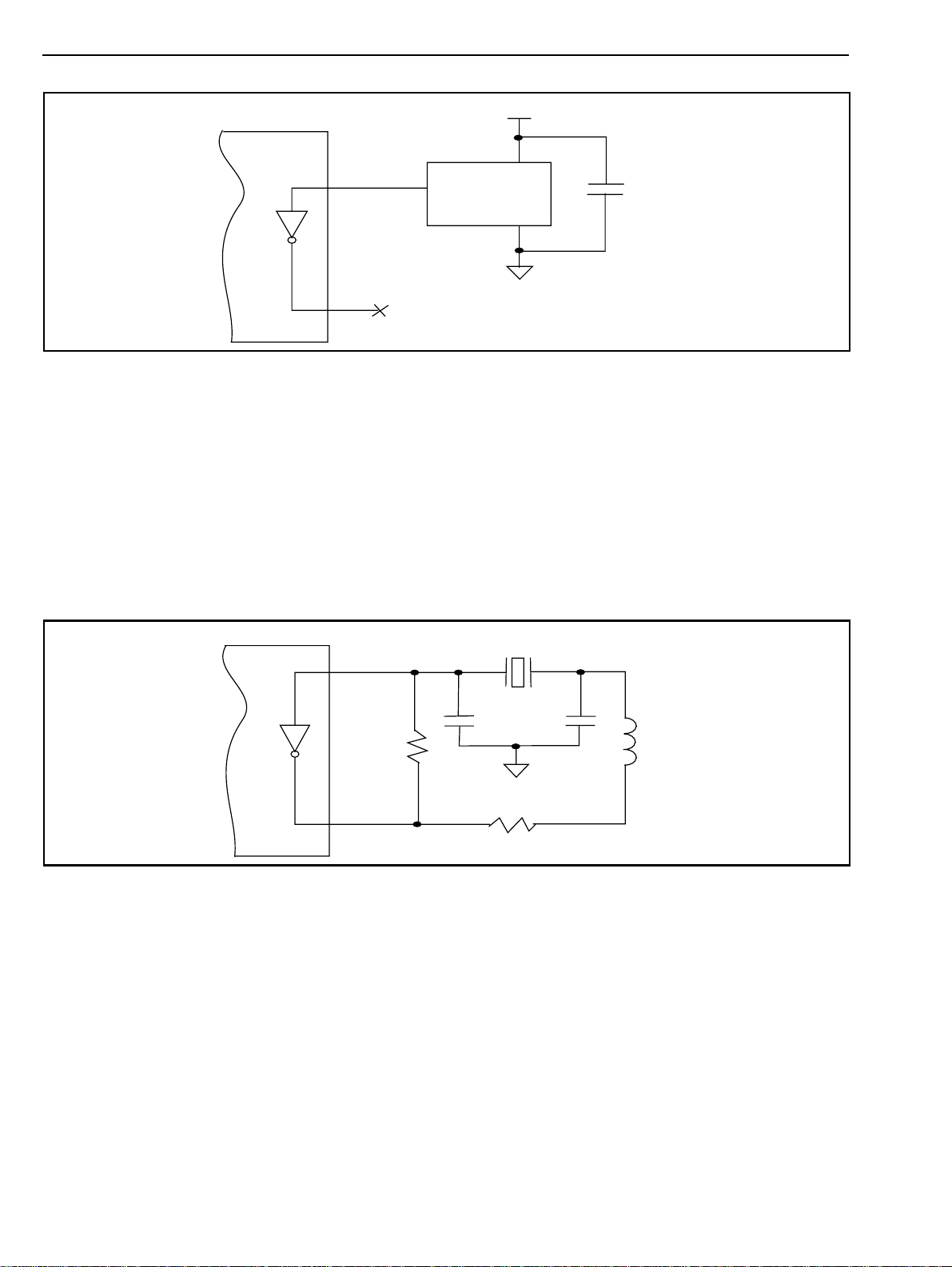
1.3 20 Mhz Clock
The MT9076 requires a 20 Mhz a clock. This may provided by a 50 ppm oscillator as per Figure 10.
21
Page 26
MT9076 Preliminary Information
+3.3V
OSC1
OSC2
20MHz
OUT
(open)
Vdd
GND
.1µF
Figure 9 - Clock Oscillator Circuit
Alternatively, a crystal oscillator may be used. A complete oscillator circuit made up of a crystal, resistors and
capacitors is shown in Figure 10. The crystal specification is as follows.
Frequency: 20MHz
Tolerance: 50ppm
Oscillation Mode: Fundamental
Resonance Mode: Parallel
Load Capacitance: 32pF
Maximum Series Resistance: 35
Ω
Approximate Drive Level: 1mW
20MHz
OSC1
56pF
1MΩ
OSC2
39pF
1µH*
100Ω
Note: the 1µH inductor is optional
Figure 10 - Crystal Oscillator Circuit
1.4 Phase Lock Loop (PLL)
The MT9076 contains a PLL, which can be locked to either an input 4.096 Mhz clock or the extracted line
clock.The PLL will attenuate jitter from less than 2.5 Hz and roll-off at a rate of 20 dB/decade. Its intrinsic jitter
is less than 0.02 UI. The PLL will meet the jitter transfer characteristics as specified by AT&T document
TR 62411and the relevant recommendations as shown in Figure 12.
22
Page 27
Preliminary Information MT9076
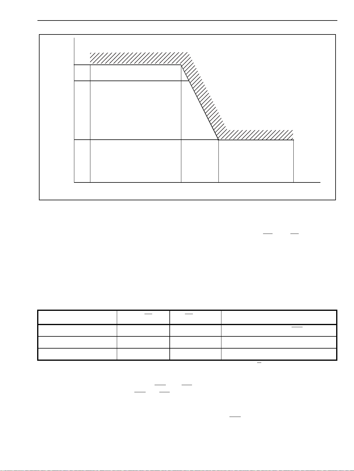
dB
-0.5
0
-20 dB/decade
JITTER ATTENUATION (dB)
19.5
10 40 400 10K
Frequency (Hz)
Figure 11 - TR 62411 Jitter Attenuation Curve
2.0 Clock Jitter Attenuation Modes
MT9076 has three basic jitter attenuation modes of operation, selected by the BS/LS and S/FR/Exclki control
pins.
• System Bus Synchronous Mode
• Line Synchronous Mode
• Free-run mode
Depending on the mode selection above, the PLL can either attenuate transmit clock jitter or the receive clock
jitter. Table 5 shows the appropriate configuration of each control pin to achieve the appropriate mode and
Jitter attenuation capability of the MT9076.
Mode Name BS/LS S/FR/Exclki Note
System Bus Synchronous 1 1 PLL locked to C4b.
Line Synchronous 0 1 PLL locked to Exclk.
Free-Run x 0 PLL free - running.
Table 5 - Selection of clock jitter attenuation modes using the M/S and MS/FR pins
In System Bus Synchronous mode, pins C4b and F0b are always configured as inputs, while in the Line
Synchronous and Free-Run modes C4b and F0b are configured as outputs.
Referring to the mode names given in Table 5 the basic operation of the jitter attenuation modes are:
•In
System Bus Synchronous
mode an external clock is applied to C4b. The applied clock is dejittered by
the internal PLL before being used to synchronize the transmitted data. The clock extracted (with no
jitter attenuation performed) from the receive data can be monitored on pin Exclk.
23
Page 28

MT9076 Preliminary Information
•In
Line Synchronous
and then output on pin C4b. Pin Exclk provides the extracted receive clock before it has been dejittered.
The transmit data is synchronous to the clean receive clock.
•In
Free-Run
is output on pin C4b. The clock signal extracted from the receive data is not dejittered and is output
directly on Exclk.
2.1 Jitter Attenuator FIFO
In System Bus Synchronous operation, a data buffer is required between the jittered input clock and the clean
transmit clock. In normal T1 mode, the transmit slip buffer performs this function. In T1 IMA mode, the transmit
slip buffer is unused, instead a jitter attenuator FIFO is employed. In an E1 mode System Bus Synchronous
configuration, the jitter attenuator FIFO is always used. In this case the C4b signal clocks the data into the
FIFO, the PLL de-jitters the C4b clock and the resulting clean C4b signal clocks the data out of the FIFO.
The JA meets the jitter transfer characteristics as proposed by ETSI ETS 300 011, G.735 and the relevant
recommendations as shown in Figure 12. The JA FIFO depth can be selected to be from 16 to 128 words deep ,
in multiples of 16 (2-bit) words. Its read pointer can be centered by changing the JFC bit (address 13H of page
02H) to provide maximum jitter tolerance. If the read pointer should come within 4 bits of either end of the
FIFO, the read clock frequency will be increased or decreased by 0.0625 UI to correct the situation. The
maximum time needed to centre is T
this time the JA will not attenuate jitter.
mode the transmit data is synchronized to the internally generated clock. The internal clock
mode, the clock extracted from the receive data is dejittered using the internal PLL
= 3904∗Depth ns, where Depth is the selected JA FIFO depth. During
max
2.2 IMA Mode
2.2.1 T1 Mode
In T1 IMA Mode, neither the transmit nor the receive slip buffers are activated. Channel Associated signaling
(CAS) and HDLC operation is not supported. The input pin C4b accepts a 1.544 MHz clock and it clocks
incoming data from DSTi into a jitter attenuator FIFO. This clock is dejittered with the internal PLL. The
dejittered clock clocks data out of the FIFO for transmission onto the line. Receive clock (1.544 MHz) and data
is extracted from the line and routed to pins Exclk and DSTo respectively. The receive clock Exclk is not
dejittered before being driven off chip. For operation in IMA mode, the MT9076 should be programmed in
System Bus Synchronous mode (BS/LS and S/FR/Exclki set high).
2.2.2 E1 Mode
In E1 IMA Mode neither the transmit nor the receive slip buffers are activated. The input pin C4b accepts a
2.048 MHz clock and it clocks incoming data from DSTi into a jitter attenuator FIFO. This clock is dejittered with
the internal PLL. The dejittered clock clocks data out of the FIFO for transmission onto the line. Receive clock
(2.048 MHz) and data is extracted from the line and routed to pins Exclk and DSTo respectively. The receive
clock Exclk is not dejittered before being driven off chip. For operation in IMA mode, the MT9076 should be
programmed in System Bus Synchronous mode (BS/LS and S/FR/Exclki set high).
3.0 The Digital Interface
3.1 T1 Digital Interface
In T1 mode, DS1 frames are 193 bits long and are transmitted at a frame repetition rate of 8000 Hz, which
results in an aggregate bit rate of 193 bits x 8000/sec= 1.544 Mbits/sec. The actual bit rate is 1.544 Mbits/sec
+/-50 ppm optionally encoded in B8ZS format. The Zero Suppression control register (page 1, address 15H,)
selects either B8ZS encoding, forced one stuffing or alternate mark inversion (AMI) encoding. Basic frames are
divided into 24 time slots numbered 1 to 24. Each time slot is 8 bits in length and is transmitted most significant
bit first (numbered bit 1). This results in a single time slot data rate of 8 bits x 8000/sec. = 64 kbits/sec.
24
Page 29

Preliminary Information MT9076
It should be noted that the Mitel ST-BUS has 32 channels numbered 0 to 31. When mapping to the DS1
payload only the first 24 time slots and the last (time slot 31, for the overhead bit) of an ST-BUS are used (see
Table 6). All unused channels are tristate.
When signaling information is written to the MT9076 in T1 mode using ST-BUS control links (as opposed to
direct writes by the microport to the on - board signaling registers), the CSTi channels corresponding to the
selected DSTi channels streams are used to transmit the signaling bits.
Since the maximum number of signaling bits associated with any channel is 4 (in the case of ABCD), only half
a CSTi channel is required for sourcing the signaling bits. The choice of which half of the channel to use is
selected by the control bit MSN (page 01H address 14H). The same control bit selects which half of the CSTo
channel will contain receive signaling information (the other nibble in the channel being tristate). Unused
channels are tristate.
The most significant bit of an eight bit ST-BUS channel is numbered bit 7 (see Mitel Application Note MSAN-
126). Therefore, ST-BUS bit 7 is synonymous with DS1 bit 1; bit 6 with bit 2: and so on.
DS1 Timeslots 12345678910111213141516
Voice/Data Channels
(DSTi/o and CSTi/o)
Ds1 Timeslots 17 18 19 20 21 22 23 24 ------- Voice/Data Channels
(DSTi/o and CSTi/o)
3.2 Frame and Superframe Structure in T1 mode
3.2.1 Multiframing
In T1 mode, DS1 trunks contain 24 bytes of serial voice/data channels bundled with an o verhead bit. The frame
overhead bit contains a fixed repeating pattern used to enable DS1 receivers to deliniate frame boundaries.
Overhead bits are inserted once per frame at the beginning of the transmit frame boundary. The DS1 frames
are further grouped in bundles of frames, generally 12 (for D4 applications) or 24 frames (for ESF - extended
superframe applications) deep. Table 7 and 8 illustrate the D4 and ESF frame structures respectively.
For D4 links the frame structure contains an alternating 101010... pattern inser ted into every second overhead
bit position. These bits are intended for determination of frame boundaries, and they are referred to as Ft bits.
A separate fixed pattern, repeating every superframe, is interleaved with the Ft bits. This fixed pattern
(001110), is used to deliniate the 12 frame superframe. These bits are referred to as the Fs bits. In D4 frames
# 6 and #12, the LSB of each channel byte may be replaced with A bit (frame #6) and B bit (frame #12)
signaling information.
0123456779101112131415
16 17 18 19 20 21 22 23 24x25x26x27x28x29x30x31
Sbit
Table 6 - ST-BUS vs. DS1 to Channel Relationship(T1)
For ESF links the 6 bit framing pattern 001011, inserted into every 4th overhead bit position, is used to
deliniate both frame and superframe boundaries. Frames #6, 12, 18 and 24 contain the A, B, C and D signaling
bits, respectively. A 4 kHz data link is embedded in the overhead bit position, interleaved between the framing
pattern sequence (FPS) and the transmit CRC-6 remainder (from the calculation done on the previous
superframe), see Table 8.
The SLC-96 frame structure is similar to the D4 frame structure, except a facility management overlay is
superimposed over the erstwhile Fs bits, see Table 9.
The protocol appropriate for the application is selected via the Framing Mode Selection Word, address 10H of
Master Control page 1. In T1 mode, MT9076 is capable of generating the overhead bit framing pattern and (for
ESF links) the CRC remainder for transmission onto the DS1 trunk. The beginning of the transmit multiframe
may be determined by any of the following criteria:
25
Page 30

MT9076 Preliminary Information
(i) It may free - run with the internal multiframe counters;
(ii) The multiframe counters may be reset with the external hardware pin TxMF. If this signal is not
synchronous with the current transmit frame count it may cause the far end to go temporarily out of sync.
(iii) Under software control (by setting the TxSYNC bit in page 01 address 12H) the transmit multiframe
counters will be synchronized to the framing pattern present in the overhead bits multiplexed into channel
31 bit 0 of the incoming 2.048 Mb/s digital stream DSTi. Note that the overhead bits extracted from the
receive signal are multiplexed into outgoing DSTo channel 31 bit 0.
(iv) In SLC - 96 mode the transmit frame counters synchronize to the framing pattern clocked in on the TXDL
input
Frame # Ft Fs Signaling
11
20
30
40
51
61A
70
81
91
10 1
11 0
12 0 B
Table 7 - D4 Superframe Structure(T1)
Frame # FPS FDL CRC Signaling
1X
2 CB1
3X
40
5X
6 CB2 A
7X
80
9X
10 CB3
11 X
12 1 B
13 X
14 CB4
15 X
16 0
17 X
18 CB5 C
19 X
20 1
21 X
22 CB6
23 X
24 1 D
Table 8 - ESF Superframe Structure (T1)
26
Page 31

Preliminary Information MT9076
Frame # Ft Fs Notes Frame # Ft Fs Notes Frame # Ft Fs Notes
1 1 25 1 C 49 1
2 0 R 26 X o 50 S S = Spoiler Bits
3 0 e270 n510
4 0s28Xc52S
5 1 y291 e531
6 0 n 30 X n 54 C C = Maintenance Field Bits
7 0 c310 t 550
81h32Xr56C
9 1 r 331 a571
10 1 o 34 X t 58 C
11 0 n 35 0 o 59 0
12 1 i 36 X r 60 A A = Alarm Field Bits
13 1 z 37 1 61 1
14 0 a 38 X F 62 A
15 0 t 39 0 i 63 0
16 0 i 40 X e 64 L L = Line Switch Field Bits
17 1 o 41 1 l 65 1
18 0 n 42 X d 66 L
19 0 43 0 67 0
20 1 d 44 X B 68 L
21 1 a 45 1 i 69 1
22 1 t 46 X t 70 L
23 0 a 47 0 s 71 0
24 1 48 S 72 S S = Spoiler Bits
Table 9 - SLC-96 Framing Structure(T1)
3.3 E1 Digital Interface
PCM 30 (E1) basic frames are 256 bits long and are transmitted at a frame repetition rate of 8000 Hz, which
results in an aggregate bit rate of 256 bits x 8000/sec = 2.048 Mbits/sec. The actual bit rate is 2.048 Mbits/sec
+/-50 ppm encoded in HDB3 format. The HDB3 control bit (page 01H, address 15H, bit 5) selects either HDB3
encoding or alternate mark inversion (AMI) encoding. Basic frames are divided into 32 time slots numbered 0
to 31, see Figure 31. Each time slot is 8 bits in length and is transmitted most significant bit first (numbered bit
1). This results in a single time slot data rate of 8 bits x 8000/sec. = 64 kbits/sec.
It should be noted that the Mitel ST-BUS also has 32 channels numbered 0 to 31, but the most significant bit of
an eight bit channel is numbered bit 7 (see Mitel Application Note MSAN-126). Therefore, ST-BUS bit 7 is
synonymous with PCM 30 bit 1; bit 6 with bit 2: and so on (Figure 31).
PCM 30 time slot 0 is reserved for basic frame alignment, CRC-4 multiframe alignment and the
communication of maintenance information. In most configurations time slot 16 is reserved for either Channel
Associated signaling (CAS or ABCD bit signaling) or Common Channel signaling (CCS). The remaining 30
time slots are called channels and carry either PCM encoded voice signals or digital data. Channel alignment
and bit numbering is consistent with time slot alignment and bit numbering. However, channels are numbered 1
to 30 and relate to time slots as per Table 10.
PCM 30 Timeslots 0 1,2,3...15 16 17,18,19,... 31
Voice/Data Channels
(DSTi/o and CSTi/o)
0 1,2,3...15 16 17,18,19,... 31
Table 10 - ST-BUS vs. PCM-30 to Channel Relationship(E1)
27
Page 32

MT9076 Preliminary Information
a
3.3.1 Basic Frame Alignment
Time slot 0 of every basic frame is reserved for basic frame alignment and contains either a Frame Alignment
Signal (FAS) or a Non-Frame Alignment Signal (NFAS). FAS and NFAS occur in time slot zero of consecutive
basic frames as shown in Table 12. Bit two is used to distinguish between FAS (bit two = 0) and NFAS (bit two
= 1).
Basic frame alignment is initiated by a search for the bit sequence 0011011 which appears in the last seven bit
positions of the FAS, see the Frame Algorithm section. Bit position one of the FAS can be either a CRC-4
remainder bit or an international usage bit.
Bits four to eight of the NFAS (i.e., Sa4 - Sa8) are additional spare bits which may be used as follows:
•Sa4 to Sa8 may be used in specific point-to-point applications (e.g. transcoder equipments conforming to
G.761)
•Sa4 may be used as a message-based data link for operations, maintenance and performance
monitoring
•Sa5to Sa8 are for national usage
A maintenance channel or data link at 4,8,12,16,or 20 kHz for selected Sa bits is provided by the MT9076 in E1
mode to implement these functions. Note that for simplicity all Sa bits including Sa4 are collectively called
national bits throughout this document.
Bit three (designated as “A”), the Remote Alarm Indication (RAI), is used to indicate the near end basic frame
synchronization status to the far end of a link. Under normal operation, the A (RAI) bit should be set to 0, while
in alarm condition, it is set to 1.
Bit position one of the NFAS can be either a CRC-4 multiframe alignment signal, an E-bit or an international
usage bit. Refer to an approvals laboratory and national standards bodies for specific requirements.
CRC
Sub Multi Frame 1
Sub Multi Frame 2
CRC
Frame/Type
0/FAS C
12345678
1
0011011
1/NFAS 01ASa4S
2/FAS C
2
0011011
3/NFAS 01ASa4S
4/FAS C
3
0011011
5/NFAS 11ASa4S
6/FAS C
4
0011011
7/NFAS 01ASa4S
8/FAS C
1
0011011
9/NFAS 11ASa4S
10/FAS C
2
0011011
11/NFAS 11ASa4S
12/FAS C
13/NFAS E
14/FAS C
15/NFAS E
3
1
4
2
0011011
1ASa4S
0011011
1ASa4S
PCM 30 Channel Zero
a5
a5
a5
a5
a5
a5
a5
a5
S
a6
S
a6
S
a6
S
a6
S
a6
S
a6
S
a6
S
a6
S
a7
S
a7
S
a7
S
a7
S
a7
S
a7
S
a7
S
a7
S
a8
S
a8
S
a8
S
a8
S
a8
S
a8
S
a8
S
a8
Table 11 - FAS and NFAS Structure
28
indicates position of CRC-4 multiframe alignment sign
Page 33

Preliminary Information MT9076
3.3.2 CRC-4 Multiframing in E1 mode
The primary pur pose for CRC-4 multiframing is to provide a verification of the current basic frame alignment,
although it can also be used for other functions such as bit error rate estimation. The CRC-4 multiframe
consists of 16 basic frames numbered 0 to 15, and has a repetition rate of 16 frames X 125 microseconds/
frame = 2 msec.
CRC-4 multiframe alignment is based on the 001011 bit sequence, which appears in bit position one of the first
six NFASs of a CRC-4 multiframe.
The CRC-4 multiframe is divided into two submultiframes, numbered 1 and 2, which are each eight basic
frames or 2048 bits in length.
The CRC-4 frame alignment verification functions as follows. Initially, the CRC-4 operation must be activated
and CRC-4 multiframe alignment must be achieved at both ends of the link. At the local end of a link, all the bits
of every transmit submultiframe are passed through a CRC-4 polynomial (multiplied by X4 then divided by X4 +
X + 1), which generates a four bit remainder. This remainder is inserted in bit position one of the four FASs of
the following submultiframe before it is transmitted (see Table 12).
The submultiframe is then transmitted and, at the far end, the same process occurs. That is, a CRC-4
remainder is generated for each received submultiframe. These bits are compared with the bits received in
position one of the four FASs of the next received submultiframe. This process takes place in both directions of
transmission.
When more than 914 CRC-4 errors (out of a possible 1000) are counted in a one second interval, the framing
algorithm will force a search for a new basic frame alignment. See Frame Algorithm section for more details.
The result of the comparison of the received CRC-4 remainder with the locally generated remainder will be
transported to the far end by the E-bits. Therefore, if E1 = 0, a CRC-4 error was discovered in a submultiframe
1 received at the far end; and if E2 = 0, a CRC-4 error was discovered in a submultiframe 2 received at the far
end. No submultiframe sequence numbers or re-transmission capabilities are supported with layer 1 PCM 30
protocol. See ITU-T G.704 and G.706 for more details on the operation of CRC-4 and E-bits.
There are two CRC multiframe alignment algorithm options selected by the AUTC control bit (address 10H,
page 01H). When AUTC is zero, automatic CRC-to-non-CRC interworking is selected. When AUTC is one and
ARAI is low, if CRC-4 multiframe alignment is not found in 400 msec, the transmit RAI will be continuously high
until CRC-4 multiframe alignment is achieved.
The control bit for transmit E bits (TE, address 11H of page 01H) will have the same function in both states of
AUTC. That is, when CRC-4 synchronization is not achieved the state of the transmit E-bits will be the same as
the state of the TE control bit. When CRC-4 synchronization is achieved the transmit E-bits will function as per
ITU-T G.704. Table 12 outlines the operation of the AUTC, ARAI and TALM control bits of the MT9076.
29
Page 34

MT9076 Preliminary Information
AUTC ARAI TALM Description
0 0 X Automatic CRC-interworking is activated. If no valid CRC MF AS is being receiv ed,
transmit RAI will flicker high with every reframe (8msec.), this cycle will continue
for 400 msec., then transmit RAI will be low continuously. The device will stop
searching for CRC MFAS, continue to transmit CRC-4 remainders, stop CRC-4
processing, indicate CRC-to-non-CRC operation and transmit E-bits to be the
same state as the TE control bit (page 01H, address 16H).
0 1 0 Automatic CRC-interworking is activated. Transmit RAI is low continuously.
0 1 1 Automatic CRC-interworking is activated. Transmit RAI is high continuously.
1 0 X Automatic CRC-interworking is de-activated. If no valid CRC MFAS is being
received, transmit RAI flickers high with every reframe (8 msec.), this cycle
continues for 400 msec, then transmit RAI becomes high continuously. The
device continues to search f or CRC MFAS and transmit E-bits are the same state
as the TE control bit. When CRCSYN = 0, the CRC MFAS search is terminated
and the transmit RAI goes low.
1 1 0 Automatic CRC-interworking is de-activated. Transmit RAI is low continuously.
1 1 1 Automatic CRC-interworking is de-activated. Transmit RAI is high continuously.
Table 12 - Operation of AUTC, ARAI and TALM Control Bits (E1 Mode)
3.3.3 CAS Signaling Multiframing in E1 mode
The purpose of the signaling multiframing algorithm is to provide a scheme that will allow the association of a
specific ABCD signaling nibble with the appropriate PCM 30 channel. Time slot 16 is reserved for the
communication of Channel Associated signaling (CAS) information (i.e., ABCD signaling bits for up to 30
channels). Refer to ITU-T G.704 and G.732 for more details on CAS multiframing requirements.
A CAS signaling multiframe consists of 16 basic frames (numbered 0 to 15), which results in a multiframe
repetition rate of 2 msec. It should be noted that the boundaries of the signaling multiframe may be completely
distinct from those of the CRC-4 multiframe. CAS multiframe alignment is based on a multiframe alignment
signal (a 0000 bit sequence), which occurs in the most significant nibble of time slot 16 of basic frame 0 of the
CAS multiframe. Bit 6 of this time slot is the multiframe alarm bit (usually designated Y). When CAS
multiframing is acquired on the receive side, the transmit Y-bit is zero; when CAS multiframing is not acquired,
the transmit Y-bit is one. Bits 5, 7 and 8 (usually designated X) are spare bits and are normally set to one if not
used.
Time slot 16 of the remaining 15 basic frames of the CAS multiframe (i.e., basic frames 1 to 15) are reserved
for the ABCD signaling bits for the 30 payload channels. The most significant nibbles are reserved for channels
1 to 15 and the least significant nibbles are reserved for channels 16 to 30. That is, time slot 16 of basic frame
1 has ABCD for channel 1 and 16, time slot 16 of basic frame 2 has ABCD for channel 2 and 17, through to
time slot 16 of basic frame 15 has ABCD for channel 15 and 30.
4.0 MT9076 Access and Control
4.1 The Control Port Interface
The control and status registers of the MT9076 are accessible through a non-multiplexed parallel
microprocessor port. The parallel por t may be configured for Motorola style control signals (by setting pin INT/
MOT low) or Intel style control signals (by setting pin INT/MOT high).
30
Page 35

Preliminary Information MT9076
4.2 Control and Status Register Access
The controlling microprocessor gains access to specific registers of the MT9076 through a two step process.
First, writing to the Command/Address Register (CAR) selects one of the 15 pages of control and status
registers (CAR address: AC4 = 0, AC3-AC0 = don't care, CAR data D7 - D0 = page number). Second, each
page has a maximum of 16 registers that are addressed on a read or write to a non-CAR address (non-CAR:
address AC4 = 1, AC3-AC0 = register address, D7-D0 = data). Once a page of memory is selected, it is only
necessary to write to the CAR when a different page is to be accessed. See the AC Electrical Characteristics
section.
Page Address D7 - D
0
00000001 (01H) Master
00000010 (02H) R/W
Control
00000011 (03H) Master
00000100 (04H) R/W
Status
Register Description Processor Access ST-BUS Access
R/W
- - -
R
- - -
00000101 (05H) Per Channel Transmit signaling R/W CSTi
00000110 (06H) Per Channel Transmit signaling R/W CSTi
00000111 (07H) Per Time Slot Control - - 00001000 (08H) Per Time Slot Control R/W - - -
00001001 (09H) Per Channel Receive signaling R/W CSTo
00001010 (0AH) Per Channel Receive signaling R/W CSTo
00001011 (0BH) HDLC0 Control and Status R/W - 00001011 (0CH) HDLC1 Control and Status R/W --00001011 (0DH) HDLC2 Control and Status R/W --00001011 (0EH) Tx National Bit Buffer R/W ---
00001011 (0FH) Rx National Bit Buffer R ---
Table 13 - Page Summary
Please note that for microprocessors with read/write cycles less than 200 ns, a wait state or a dummy oper ation
(for C programming) between two successive read/write operations to the HDLC FIFO is required.
Table 13 associates the MT9076 control and status pages with access and page descriptions.
4.3 Identification Code
The MT9076 shall be identified by the code 01111000, read from the identification code status register (page
03H, address 1FH).
4.4 ST-BUS Streams
In T1 mode, there is one control and one status ST-BUS stream that can be used to program / access channel
associated signaling nibbles. CSTo contains the received channel associated signaling bits, and for those
channels whose Per Time Slot Control word bit 1 "RPSIG" is set low, CSTi is used to control the transmit
channel associated signaling. The DSTi and DSTo streams contain the transmit and receive voice and digital
data. Only 24 of the 32 ST-BUS channels are used for each of DSTi, DSTo, CSTi and CSTo. In each case
individual channel mapping is as illustrated in Table 6, “ST-BUS vs. DS1 to Channel Relationship(T1),” on
page 25.
In E1 mode, ST-BUS streams can also be used to access channel associated signaling nibbles. CSTo contains
the received channel associated signaling bits (e.g., ITU-T R1 and R2 signaling) ,and f or those channels whose
31
Page 36

MT9076 Preliminary Information
Per Time Slot Control word bit 1 "RPSIG" is set low, CSTi is used to control the transmit channel associated
signaling. The DSTi and DSTo streams contain the transmit and receive voice and digital data.
Only 30 of the 32 ST-BUS channels are used for each of DSTi, DSTo, CSTi and CSTo. In each case individual
channel mapping is as illustrated in Table 10 Time slot to Channel Relationship.
5.0 Reset Operation (Initialization)
The MT9076 can be reset using the hardware RESET pin (pin 11 in PLCC, pin 64 in LQFP) or the software
reset bit RST (page 1H, address 1AH) . When the device emerges from its reset state it will begin to function
with the default settings described in Table 14 (T1) and Table 15 (E1). All control registers are set to 00H. A
reset operation takes 1 full frame (125 us) to complete.
Function Status
Mode D4
Loopbacks Deactivated
SLC-96 Deactivated
Zero Coding Deactivated
Line Codes Deactivated
Data Link Serial Mode
signaling CAS Registers
AB/ABCD Bit Debounce Deactivated
Interrupts masked
Error Insertion Deactivated
HDLCs Deactivated
Counters Cleared
Transmit Data All Ones
Table 14 - Reset Status(T1)
Function Status
Mode Termination
Loopbacks Deactivated
Transmit FAS Cn0011011
Transmit non-FAS 1/Sn1111111
Transmit MFAS (CAS) 00001111
Data Link Deactivated
CRC Interworking Activated
signaling CAS Registers
ABCD Bit Debounce Deactivated
Interrupts Masked
RxMF Output signaling Multiframe
Error Insertion Deactivated
HDLCs Deactivated
Counters Cleared
Transmit Data All Ones
Table 15 - Reset Status (E1)
32
Page 37

Preliminary Information MT9076
6.0 Transmit Data All Ones (TxAO) Operation
The TxAO (Transmit all ones) pin allows the PRI interface to transmit an all ones signal under hardware control.
7.0 Data Link Operation
7.1 Data Link Operation in E1 mode
In E1 mode, MT9076 has a user defined 4, 8, 12, 16 or 20 kbit/s data link for transport of maintenance and
performance monitoring information across the PCM 30 link. This channel functions using the Sa bits (Sa4~Sa8)
of the PCM 30 timeslot zero non-frame alignment signal (NFAS). Since the NFAS is transmitted every other
frame - a periodicity of 250 microseconds - the aggregate bit rate is a multiple of 4 kb/s. As there are five S
bits independently available for this data link, the bit rate will be 4, 8, 12, 16 or 20 kb/s, depending on the bits
selected for the Data Link (DL).
The Sa bits used for the DL are selected by setting the appropriate bits, Sa4~Sa8, to one in the Data Link Select
Word (page 01H, address 17H, bits 4-0). Access to the DL is provided by pins TxDLCLK, TxDL, RxDLCLK and
RxDL, which allow easy interfacing to an external controller.
Data to be transmit onto the line in the Sa bit position is clocked in from the TxDL pin (pin 65 in PLCC, pin 47 in
LQFP) with the clock TxDLCLK (pin 64 in PLCC, pin 46 pin LQFP). Although the aggregate clock rate equals
the bit rate, it has a nominal pulse width of 244 ns, and it clocks in the TxDL as if it were a 2.048 Mb/s data
stream. The clock can only be active during bit times 4 to 0 of the STBUS frame. The TxDL input signal is
clocked into the MT9076 by the rising edge of TxDLCLK. If bits are selected to be a part of the DL, all other
programmed functions for those Sa bit positions are overridden.
a
The RxDLCLK signal (pin 39 - PLCC, pin 14 - LQFP) is derived from the receive extracted clock and is aligned
with the receive data link output RxDL. The HDB3 decoded receive data, at 2.048 Mbit/s, is clocked out of the
device on pin RxDL (pin 40 in PLCC, pin 15 in LQFP). In order to facilitate the attachment of this data stream to
a Data Link controller, the clock signal RxDLCLK consists of positive pulses, of nominal width of 244 ns, during
the Sa bit cell times that are selected for the data link.This selection is made by programming address 17H of
master control page 01H. No DL data will be lost or repeated when a receive frame slip occurs. See AC
Electrical Characteristics for timing requirements.
7.2 Data Link Operation in T1 mode
SLC-96 and ESF protocol allow for carrier messages to be embedded in the overhead bit position. The
MT9076 provides 3 separate means of controlling these data links. See Data Link Control Word - address 12H,
page 1H.
• The data links (transmit and receive) may be sourced (sunk) from an external controller using dedicated
pins on the MT9076 in T1 mode (enabled by setting the bit 7 - EDL of the Data link Control Word).
• Bit Oriented Messages may be transmit and received via a dedicated TxBOM register (page 1H,
address 13H) and a RxBOM (page 3H, address 15H). Transmission is enabled by setting bit 6 - BIOMEn
in the Data link Control Word. Bit - oriented messages may be periodically interrupted (up to once per
second) for a duration of up to 100 milliseconds. This is to accommodate bursts of message - oriented
protocols. See Table 16 for message structure.
33
Page 38

MT9076 Preliminary Information
Octet # 8 7 6 5 4 3 2 1 Content
1 F L A G 01111110
2 S A P I C / R EA 00111000
or
00111010
3 T E I EA 00000001
4 C O N T R O L 00000011
5 G3LVG4U1U2G5SLG6 t0
6 FE SE LB G1 R G2 Nm NI t0
7 G3LVG4U1U2G5SLG6 t0-1
8 FE SE LB G1 R G2 Nm NI t0-1
9 G3LVG4U1U2G5SLG6 t0-2
10 FE SE LB G1 R G2 Nm NI t0-2
11 G3 LV G4 U1 U2 G5 SL G6 t0-3
12 FE SE LB G1 R G2 Nm NI t0-3
13 F C S VARIABLE
14
Table 16 - Message Oriented Performance Report Structure (T1.403 and T1.408)
Note: ADDRESS INTERPRETATION
00111000 SAPI = 14, C/R = 0 (CI) EA = 0
00111010 SAPI = 14, C/R = 1(Carrier) EA = 0
00000001 TEI = 0, EA =1
CONTROL INTERPRETATION
00000011 Unacknowledged Information Transfer
ONE SECOND REPORT INTERPRETATION
G1 = 1 CRC Error Event =1
G2 =1 1 < CRC Error Event < 5
G3 =1 5 < CRC Error Event < 10
G4 =1 10 < CRC Error Event < 100
G5 =1 100 < CRC Error Event < 319
G6 =1 CRC Error Event > 320
SE = 1 Severely - Errored Framing Event >=1
FE = 1 Frame Synchronization Bit Error Event >=1
LV = 1 Line code Violation Event >=1
SL = 1 Slip Event >=1
LB = 1 Payload Loopback Activated
U1,U2 = 0 Under Study for sync.
R = 0 Reserved - set to 0
NmNI = 00, 01, 10, 11 One Second Module 4 counter
FCS INTERPRETATION
VARIABLE CRC16 Frame Check Sequence
34
Page 39

Preliminary Information MT9076
7.2.1 External Data Link
In T1 mode, MT9076 has two pairs of pins (TxDL and TxDLCLK, RxDL and RxDLCLK) dedicated to
transmitting and receiving bits in the selected overhead bit positions. Pins TxDLCLK and RxDLCLK are clock
outputs available for clocking data into the MT9076 (for transmit) or external device (for receive information).
Each clock operates at 4 Khz. In the SLC-96 mode the optional serial data link is multiplexed into the Fs bit
position. In the ESF mode, the serial data link is multiplexed into odd frames, i.e. the FDL bit positions.
7.2.2 Bit - Oriented Messaging
In T1 mode, MT9076 Bit oriented messaging may be selected by setting bit 6 (BIOMEn) in the Data Link
Control Word (page 1H, address 12H). The transmit data link will contain the repeating serial data stream
111111110xxxxxx0 where the byte 0xxxxxx0 originates from the user programmed register "Transmit Bit
Oriented Message" - page 1H address 13H. The receive BIOM register "Receive Bit Oriented Message" - page
3H, address 15H, will contain the last received valid message (the 0xxxxxx0 portion of the incoming serial bit
stream). To prevent spurious inputs from creating false messages, a new message must be present in 7 of the
last 10 appropriate byte positions before being loaded into the receive BIOM register. When a new message
has been received, a maskable interrupt (maskable by setting bit 1 low in Interrupt Mask Word Three - page
1H, address 1EH) may occur.
8.0 Floating HDLC Channels
MT9076 has three embedded HDLC controllers (HDLC0, HDLC1, HDLC2) each of which includes the following
features:
• Independent transmit and receive FIFO's;
• Receive FIFO maskable interrupts for nearly full (programmable interrupt levels) and overflow
conditions;
• Transmit FIFO maskable interrupts for nearly empty (programmable interrupt levels) and underflow
conditions;
• Maskable interrupts for transmit end-of-packet and receive end-of-packet;
• Maskable interrupts for receive bad-frame (includes frame abort);
• Transmit end-of-packet and frame-abort functions.
Each controller may be attached to any of the active 64 Kkb/s channels (24 in the case of T1, 31 in the case of
E1). HDLC0 may also be attached to the FDL in a T1 ESF link by connecting it to phantom channel 31 when
programming the HDLC Select Word. If HDLC0 is attached to channel 0 in E1 mode, only the activated Sa bits
(as per the Multiframe and Data Selection Word) will be transmit and received by the controller.
8.1 Channel Assignment
In T1 mode, any DS1 channel can be connected to either of HDLC0,1 or 2, operating at 56 or 64 Kb/s. Setting
control bit H1R64 (address 12 H on page 01H) high selects 64 Kb/s operation for all HDLCs. Setting this bit lo w
selects 56 Kb/s for all HDLC. Interrupts from any of the HDLCs are masked when they are disconnected.
In E1 mode, all PCM-30 channels except channel 0 can be connected to either of HDLC0,1 or 2. HDLC1 and
HDLC2 operate at 64 Kb/s. HDLC0 operates at 64 kb/s when connected to any of channels 1 to 31. When
connected to channel 0 HDLC0 operates at 4, 8, 12, 16 or 20 Kb/s depending on the number of activated Sa
bits.
HDLCs can be activated by programming the HDLC Select Words (page 02H, addresses 19H, 1AH and 1BH
for HDLC0, HDLC1 and HDLC2 respectively).
35
Page 40

MT9076 Preliminary Information
8.2 HDLC Description
The HDLC handles the bit oriented packetized data transmission as per X.25 level two protocol defined by
CCITT. It provides flag and abor t sequence generation and detection, zero insertion and deletion, and Frame
Check Sequence (FCS) generation and detection. A single byte, dual byte and all call address in the received
frame can be recognized. Access to the receive FCS and inhibiting of transmit FCS for terminal adaptation are
also provided. Each HDLC controller has a 128 byte deep FIFO associated with it. The status and interrupt
flags are programmable for FIFO depths that can vary from 16 to 128 bytes in steps of 16 bytes. These and
other features are enabled through the HDLC control registers on page 0BH and 0CH.
8.2.1 HDLC Frame structure
In T1 mode or E1 mode, a valid HDLC frame begins with an opening flag, contains at least 16 bits of address
and control or information, and ends with a 16 bit FCS followed by a closing flag. Data formatted in this manner
is also referred to as a “packet”. Refer to Table 17: HDLC Frame Format
Flag (7E) Data Field FCS Flag (7E)
One Byte
01111110
All HDLC frames start and end with a unique flag sequence “01111110”. The transmitter generates these flags
and appends them to the packet to be transmitted. The receiver searches the incoming data stream for the
flags on a bit- by-bit basis to establish frame synchronization.
The data field consists of an address field, control field and information field. The address field consists of one
or two bytes directly following the opening flag. The control field consists of one byte directly following the
address field. The information field immediately follows the control field and consists of N bytes of data. The
HDLC does not distinguish between the control and information fields and a packet does not need to contain an
information field to be valid.
The FCS field, which precedes the closing flag, consists of two bytes. A cyclic redundancy check utilizing the
CRC-CCITT standard generator polynomial “X16+X12+X5+1” produces the 16-bit FCS. In the transmitter the
FCS is calculated on all bits of the address and data field. The complement of the FCS is transmitted, most
significant bit first, in the FCS field. The receiver calculates the FCS on the incoming packet address, data and
FCS field and compares the result to “F0B8”. If no transmission errors are detected and the packet between the
flags is at least 32 bits in length then the address and data are entered into the receive FIFO minus the FCS
which is discarded.
8.2.2 Data Transparency (Zero Insertion/Deletion)
Transparency ensures that the contents of a data packet do not imitate a flag, go-ahead, frame abort or idle
channel. The contents of a transmitted frame, between the flags, is examined on a bit-by-bit basis and a 0 bit is
inserted after all sequences of 5 contiguous 1 bits (including the last five bits of the FCS). Upon receiving five
contiguous 1s within a frame the receiver deletes the following 0 bit.
n Bytes
n ≥ 2
Table 17 - HDLC Frame Format
Two Bytes One Byte
01111110
8.2.3 Invalid Frames
A frame is invalid if one of the following four conditions exists (Inserted zeros are not part of a valid count):
• If the FCS pattern generated from the received data does not match the “F0B8” pattern then the last
data byte of the packet is written to the received FIFO with a ‘bad packet’ indication.
• A short frame exists if there are less than 25 bits between the flags. Short frames are ignored by the
receiver and nothing is written to the receive FIFO.
• Packets which are at least 25 bits in length but less than 32 bits between the flags are also invalid. In
this case the data is written to the FIFO but the last byte is tagged with a “bad packet” indication.
• If a frame abort sequence is detected the packet is invalid. Some or all of the current packet will reside
in the receive FIFO, assuming the packet length before the abort sequence was at least 26 bits long.
36
Page 41

Preliminary Information MT9076
8.2.4 Frame Abor t
The transmitter will abort a current packet by substituting a zero f ollo w ed b y seven contiguous 1s in place of the
normal packet. The receiver will abort upon reception of seven contiguous 1s occurring between the flags of a
packet which contains at least 26 bits.
Note that should the last received byte before the frame abort end with contiguous 1s, these are included in the
seven 1s required for a receiver abort. This means that the location of the abort sequence in the receiver may
occur before the location of the abort sequence in the originally transmitted packet. If this happens then the last
data written to the receive FIFO will not correspond exactly with the last byte sent before the frame abort.
8.2.5 Interframe Time Fill and Link Channel States
When the HDLC transmitter is not sending packets it will wait in one of two states
• Interframe Time Fill state: This is a continuous series of flags occurring between frames indicating that
the channel is active but that no data is being sent.
• Idle state: An idle Channel occurs when at least 15 contiguous 1s are transmitted or received.
• In both states the transmitter will exit the wait state when data is loaded into the transmitter FIFO.
8.2.6 Go-Ahead
A go ahead is defined as the pattern "011111110" (contiguous 7Fs) and is the occurance of a frame abort
sequence followed by a zero, outside of the boundaries of a normal packet. Being able to distinguish a proper
(in packet) frame abort sequence from one occurring outside of a packet allows a higher level of signaling
protocol which is not part of the HDLC specifications.
8.3 HDLC Functional Description
The HDLC transceiver can be reset by either the power reset input signal or by the HRST Control bit in the test
control register (software reset). When reset, the HDLC Control Registers are cleared, resulting in the
transmitter and receiver being disabled. The Receiver and Transmitter can be enabled independent of one
another through Control Register 1. The transceiver input and output are enabled when the enable control bits
in Control Register 1 are set. Transmit to receive loopback as well as a receive to transmit loopback are also
supported. Transmit and receive bit rates and enables can operate independently. In MT9076 the transceiver
can operate at a continuous rate independent of RXcen and TXcen (free run mode) by setting the Frun bit of
Control Register 1.
Received packets from the serial interface are sectioned into bytes by an HDLC receiver that detects flags,
checks for go-ahead signals, removes inserted zeros, performs a cyclical redundancy check (CRC) on
incoming data, and monitors the address if required. Packet reception begins upon detection of an opening
flag. The resulting bytes are concatenated with two status bits (RQ9, RQ8) and placed in a receiver first-in-firstout (Rx FIFO); a buffer register that generates status and interrupts for microprocessor read control.
In conjunction with the control circuitry, the microprocessor writes data bytes into a Tx buffer register (Tx FIFO)
that generates status and interrupts. Packet transmission begins when the microprocessor writes a byte to the
Tx FIFO. Two status bits are added to the Tx FIFO for transmitter control of frame aborts (FA) and end of
packet (EOP) flags. Packets have flags appended, zeros inserted, and a CRC, also referred to as frame
checking sequence (FCS), added automatically during serial transmission. When the Tx FIFO is empty and
finished sending a packet, Interframe Time Fill bytes (continuous flags (7E hex)), or Mark Idle (continuous
ones) are transmitted to indicate that the channel is idle.
8.3.1 HDLC Transmitter
Following initialization and enabling, the transmitter is in the Idle Channel state (Mark Idle), continuously
sending ones. Interframe Time Fill state (Flag Idle) is selected by setting the Mark idle bit in Control Register 1
high. The Transmitter remains in either of these two states until data is written to the Tx FIFO. Control Register
1 bits EOP (end of packet) and FA (Frame Abort) are set as status bits before the microprocessor loads 8 bits
of data into the 10 bit wide FIFO (8 bits data and 2 bits status). To change the tag bits being loaded in the FIFO ,
Control Register 1 must be written to before writing to the FIFO. Ho w ever, EOP and FA are reset after writing to
37
Page 42

MT9076 Preliminary Information
the TX FIFO. The Transmit Byte Count Registers may also be used to tag an end of packet. The total packet
size may be programmed to be up to 65,535 bytes. For a packet length of 1 to 255 bytes it is only necessary to
write the packet size into the Lower Transmit Byte Count Register. For a packet length of 256 to 65,535 bytes it
is necessary to write the 16 bit binar y count into the Extended Transmit Byte Count Register (MSByte) and the
Lower Transmit Byte Count Register (LSByte). Note that the order of writing the upper byte before the lower
byte must be observed even when the lower byte is all zero. Internal registers are loaded with the number of
bytes in the packet and decremented after every write to the Tx FIFO. When a count of one is reached, the next
byte written to the FIFO is tagged as an end of packet. The register may be made to cycle through the same
count if the packets are of the same length by setting Control Register 2 bit Cycle.
If the transmitter is in the Idle Channel state when data is written to the Tx FIFO, then an opening flag is sent
and data from Tx FIFO follows. Otherwise, data bytes are transmitted as soon as the current flag byte has been
sent. Tx FIFO data bytes are continuously transmitted until either the FIFO is empty or an EOP or FA status bit
is read by the transmitter. After the last bit of the EOP byte has been transmitted, a 16-bit FCS is sent followed
by a closing flag. When multiple packets of data are loaded into Tx FIFO, only one flag is sent between
packets.
Frame aborts (the transmission of 7F hex), are transmitted by tagging a byte previously written to the Tx FIFO.
When a byte has an FA tag, then an FA is sent instead of that tagged byte. That is, all bytes previous to but not
including that byte are sent. After a Frame Abort, the transmitter returns to the Mar k Idle or Interframe Time Fill
state, depending on the state of the Mark idle control bit.
Tx FIFO underrun will occur if the FIFO empties and the last byte did not have either an EOP or FA tag. A
frame abort sequence will be sent when an underrun occurs.
Below is an example of the transmission of a three byte packet (’AA’ ’03’ ’77’ hex) (Interframe time fill). TXcen
can be enabled before or after this sequence.
(a) Write ’04’hex to Control Register 1 -Mark idle bit set
(b) Write ’AA’ hex to TX FIFO -Data byte
(c) Write ’03’hex to TX FIFO -Data byte
(d) Write ’34’hex to Control Register 1 -TXEN; EOP; Mark idle bits set
(e) Write ’77’hex to TX FIFO -Final data byte
The transmitter may be enabled independently of the receiver. This is done by setting the TXEN bit of the
Control Register. Enabling happens immediately upon writing to the register. Disabling using TXen will occur
after the completion of the transmission of the present packet; the contents of the FIFO are not cleared.
Disabling will consist of stopping the transmitter clock. The Status and Interrupt Registers may still be read and
the FIFO and Control Registers may be written to while the transmitter is disabled. The transmitted FCS may
be inhibited using the Tcrci bit of Control Register 2. In this mode the opening flag followed by the data and
closing flag is sent and zero insertion still included, but no CRC. That is, the FCS is injected by the
microprocessor as part of the data field. This is used in V.120 terminal adaptation for synchronous protocol
sensitive UI frames.
8.3.2 HDLC Receiver
After initialization and enabling, the receiver clocks in serial data, continuously checking for Go-aheads (0 1111
1110), flags (0111 1110), and Idle Channel states (at least fifteen ones). When a flag is detected, the receiver
synchronizes itself to the serial stream of data bits, automatically calculating the FCS. If the data length
between flags after zero removal is less than 25 bits, then the packet is ignored so no bytes are loaded into Rx
FIFO. When the data length after zero removal is between 25 and 31 bits, a first byte and bad FCS code are
loaded into the Rx FIFO (see definition of RQ8 and RQ9 below). For an error-free packet, the result in the CRC
register should match the HEX pattern of ’F0B8’ when a closing flag is detected.
If address recognition is required, the Receiver Address Recognition Registers are loaded with the desired
address and the Adrec bit in the Control Register 1 is set high. Bit 0 of the Address Registers is used as an
enable bit for that b yte , thus allo wing either or both of the first tw o bytes to be compared to the expected values .
Bit 0 of the first byte of the address received (address e xtension bit) will be monitored to determine if a single or
38
Page 43

Preliminary Information MT9076
dual byte address is being received. If this bit is 0 then a two byte address is being received and then only the
first six bits of the first address byte are compared. An all call condition is also monitored for the second
address byte; and if received the first address byte is ignored (not compared with mask byte). If the address
extension bit is a 1 then a single byte address is being received. In this case, an all call condition is monitored
for in the first byte as well as the mask byte written to the comparison register and the second byte is ignored.
Seven bits of address comparison can be realized on the first byte if this is a single byte address by setting the
Seven bit of Control Register 2.
The following two Status Register bits (RQ8 and RQ9) are appended to each data byte as it is written to the Rx
FIFO. They indicate that a good packet has been received (good FCS and no frame abort), or a bad packet
with either incorrect FCS or frame abort. The Status and Interrupt Registers should be read before reading the
Rx FIFO since status and interrupt information correspond to the byte at the output of the FIFO (i.e. the byte
about to be read). The Status Register bits are encoded as follows:
RQ9 RQ8 Byte status
1 1 last byte (bad packet)
0 1 first byte
1 0 last byte (good packet)
0 0 packet byte
The end-of-packet-detect (EOPD) interrupt indicates that the last byte written to the Rx FIFO was an EOP byte
(last byte in a packet). The end-of-packet-read (EopR) interrupt indicates that the byte about to be read from
the Rx FIFO is an EOP byte (last byte in a packet). The Status Register should be read to see if the packet is
good or bad before the byte is read.
A minimum size packet has an 8-bit address, an 8-bit control byte, and a 16-bit FCS pattern between the
opening and closing flags (see Section 9.3.2). Thus, the absence of a data transmission error and a frame
length of at least 32 bits results in the receiver writing a valid packet code with the EOP byte into Rx FIFO. The
last 16 bits before the closing flag are regarded as the FCS pattern and will not be transferred to the receiver
FIFO. Only data bytes (Address, Control, Information) are loaded into the Rx FIFO.
In the case of an Rx FIFO overflow, no clocking occurs until a new opening flag is received. In other words, the
remainder of the packet is not clocked into the FIFO. Also, the top byte of the FIFO will not be written over. If
the FIFO is read before the reception of the next packet then reception of that packet will occur. If two
beginning of packet conditions (RQ9=0;RQ8=1) are seen in the FIFO, without an intermediate EOP status,
then overflow occurred for the first packet.
The receiver may be enabled independently of the transmitter. This is done by setting the RXEN bit of Control
Register 1. Enabling happens immediately upon writing to the register. Disabling using RXEN will occur after
the present packet has been completely loaded into the FIFO. Disabling can occur during a packet if no bytes
have been written to the FIFO yet. Disabling will consist of disabling the internal receive clock. The FIFO,
Status, and Interrupt Registers may still be read while the receiver is disabled. Note that the receiver requires a
flag before processing a frame, thus if the receiver is enabled in the middle of an incoming packet it will ignore
that packet and wait for the next complete one.
The receive CRC can be monitored in the Rx CRC Registers. These registers contain the actual CRC sent by
the other transmitter in its original form; that is, MSB first and bits inverted. These registers are updated by
each end of packet (closing flag) received and therefore should be read when an end of packet is received so
that the next packet does not overwrite the registers.
39
Page 44

MT9076 Preliminary Information
9.0 Slip Buffers
9.1 Slip Buffer in T1 Mode
In T1 mode, MT9076 contains two slip buffers, one on the transmit side, and one on the receive side. Both
sides may perform a controlled slip. The mechanisms that govern the slip function are a function of backplane
timing and the mapping between the ST-BUS channels and the DS1 channels. The slip mechanisms are
different for the transmit and receive slip buffers. The extracted 1.544 Mhz clock (Exclk) and the internally
generated transmit 1.544 Mhz clock are distinct. Slips on the transmit side are independent from slips on the
receive side. In IMA mode neither the transmit nor receive slip buffer is activated.
The transmit slip buffer has data written to it from the near end 2.048 Mb/s stream. The data is clocked out of
the buffer using signals derived from the transmit 1.544 Mhz clock. The transmit 1.544 Mhz clock is always
phase locked to the DSTi 2.048 Mb/s stream. If the system 4.096 Mhz clock (C4b) is internally generated (pin
BS/LS low), then it is hard locked to the 1.544 Mhz clock. No phase drift or wander can exist between the two
signals - therefore no slips will occur. The delay through the transmit elastic buffer is then fixed, and is a
function of the relative mapping between the DSTi channels and the DS1 timeslots. These delays vary with the
position of the channel in the frame. For example, DS1 timeslot 1 sits in the elastic buffer for approximately 1
usec and DS1 timeslot 24 sits in the elastic buffer for approximately 32 usec.
0 uS
Write
Pointer
Read Pointer
221 uS
Read Pointer
4 uS
92 uS
Wander Tolerance
512 Bit
188 uS
Read Vectors
Minimum Delay
Write Vectors
Read Vectors - Maximum Delay
Elastic
Store
129 uS
Read Pointer
Frame 0 Frame 1
Read Pointer
Frame 0 Frame 1
96 uS
62 uS
92 uS
Frame 0
Frame 1
Figure 12 - Read and Write Pointers in the Transmit Slip Buffers
If the system 4.096 Mhz clock (C4b) is externally generated (pin BS/LS high), the transmit 1.544 Mhz clock is
phase locked to it, but the PLL is designed to filter jitter present in the C4b clock. As a result phase drift will
result between the two signals. The delay through the transmit elastic buffer will vary in accordance with the
input clock drift, as well as being a function of the relative mapping between the DSTi channels and the DS1
timeslots. If the read pointers approach the write pointers (to within approximately 1 usec) or the delay through
the transmit buffer exceeds 218 usecs a controlled slip will occur. The contents of a single frame of DS1 data
will be skipped or repeated; a maskable interrupt (masked by setting bit 1 - TxSLPI high in Interrupt Mask Word
Zero - page 1H, address 1bH) will be generated, and the status bit TSLIP (page 3H, address 17H) of MSB
Transmit Slip Buffer register will toggle. The direction of the slip is indicated by bit 6 of the same register
(TSLPD). The relative phase delay between the system frame boundary and the transmit elastic frame read
40
Page 45

Preliminary Information MT9076
boundary is measured every frame and reported in the Transmit Slip Buffer Delay register- (page 3H, address
17H). In addition the relative offset between these frame boundaries may be programmed by writing to this
register. Every write to Transmit Elastic Buffer Set Delay Word resets the transmit elastic frame count bit
TxSBMSB (address 17H, page 3H). After a write the delay through the slip buffer is less than 1 frame in
duration. Each write operation will result in a disturbance of the transmit DS1 frame boundary, causing the far
end to go out of sync. Writing BC (hex) into the TxSBDLY register maximizes the wander tolerance before a
controlled slip occurs. Under normal operation no slips should occur in the transmit path. Slips will only occur if
the input C4b clock has excess wander, or the Transmit Elastic Buffer Set Delay Word register is initialized too
close to the slip pointers after system initialization.
The two frame receive elastic b uffer is attached between the 1.544 Mbit/s DS1 receive side and the 2.048 Mbit/
s ST-BUS side of the MT9076. Besides performing rate conversion, this elastic buffer is configured as a slip
buffer which absorbs wander and low frequency jitter in multi-trunk applications. The received DS1 data is
clocked into the slip buffer with the Exclk clock and is clocked out of the slip buffer with the system C4b clock.
The Exclk extracted clock is generated from, and is therefore phase-locked with, the receive DS1 data. In the
case of Internal mode (pin BS/LS set low) operation, the Exclk clock may be phase-locked to the C4b clock by
an internal phase locked loop (PLL). Therefore, in a single trunk system the receive data is in phase with the
Exclk clock, the C4b clock is phase locked to the E1.5o clock, and the read and write positions of the slip buffer
track each other.
In a multi-trunk slave or loop-timed system (i.e., PABX application) a single trunk will be chosen as a network
synchronizer, which will function as described in the previous paragraph. The remaining trunks will use the
system timing derived from the synchronizer to clock data out of their slip buffers. Even though the DS1 signals
from the network are synchronous to each other, due to multiplexing, transmission impairments and route
diversity, these signals may jitter or wander with respect to the synchronizing trunk signal. Therefore, the Exclk
clocks of non-synchronized trunks may wander with respect to the Exclk clock of the synchronizer and the
system bus. Network standards state that, within limits, trunk interfaces must be able to receive error-free data
in the presence of jitter and wander (refer to network requirements for jitter and wander tolerance). The
MT9076 will allow 92 usec (140 UI, DS1 unit intervals) of wander and low frequency jitter before a frame slip
will occur.
When the C4b and the Exclk clocks are not phase-locked, the rate at which data is being written into the slip
buffer from the DS1 side may differ from the rate at which it is being read out onto the ST-BUS. If this situation
persists, the delay limits stated in the previous paragraph will be violated and the slip buffer will perform a
controlled frame slip. That is, the buffer pointers will be automatically adjusted so that a full DS1 frame is either
repeated or lost. All frame slips occur on frame boundaries.
The minimum delay through the receive slip buffer is approximately 1 usec and the maximum delay is
approximately 249 uS. Figure 14 illustrates the relationship between the read and write pointers of the receive
slip buffer (contiguous time slot mapping). Measuring clockwise from the write pointer, if the read page pointer
comes within 8 usec of the write page pointer a frame slip will occur, which will put the read page pointer 157
usec from the write page pointer. Conversely, if the read page pointer moves more than 249 usec from the write
page pointer, a slip will occur, which will put the read page pointer 124 usec from the write page pointer. This
provides a worst case hysteresis of 92 usec peak = 142 U.I.
41
Page 46

MT9076 Preliminary Information
0 uS
Write
Pointer
Read Pointer
221 uS
Read Pointer
4 uS
92 uS
Wander Tolerance
512 Bit
188 uS
Read Vectors
Minimum Delay
Write Vectors
Read Vectors - Maximum Delay
Elastic
Store
129 uS
Read Pointer
Frame 0 Frame 1
Read Pointer
Frame 0 Frame 1
96 uS
62 uS
92 uS
Frame 0
Frame 1
Figure 13 - Read and Write Pointers in the Transmit Slip Buffers
The RSLIP and RSLPD status bits (page 3H, address 13H, bits 7 and 6 respectively) give indication of a
receive slip occurance and direction. A maskable interrupt RxSLPI (page 1H, address 1BH, bit 0 - set high to
mask) is also provided. RSLIP changes state in the event of a slip. If RSLPD=0, the slip buffer has overflowed
and a frame was lost; if RSLPD=1, a underflow condition occurred and a frame was repeated.
9.2 Slip Buffer in E1 mode
In E1 mode, in addition to the elastic buffer in the jitter attenuator(JA), another elastic buffer (two frames deep)
is present, attached between the receive side and the ST-BUS side of the MT9076. This elastic buffer is
configured as a slip buffer which absorbs wander and low frequency jitter in multi-trunk applications. The
received PCM 30 data is clocked into the slip buffer with the Exclk clock and is cloc ked out of the slip buffer with
the C4b clock. The Exclk extracted clock is generated from, and is therefore phase-locked with, the receive
PCM 30 data. In normal operation, the C4b clock will be phase-locked to the Exclk clock by a phase locked loop
(PLL). Therefore, in a single trunk system the receive data is in phase with the Exclk clock, the C4b clock is
phase-locked to the Exclk clock, and the read and write positions of the slip b uffer will remain fixed with respect
to each other.
In a multi-trunk slave or loop-timed system (i.e., PABX application) a single trunk will be chosen as a network
synchronizer, which will function as described in the previous paragraph. The remaining trunks will use the
system timing derived from the synchronizer to clock data out of their slip buffers. Even though the PCM 30
signals from the network are synchronous to each other, due to multiplexing, transmission impairments and
route diversity, these signals may jitter or wander with respect to the synchronizing trunk signal. Therefore, the
Exclk clocks of non-synchronizer trunks may wander with respect to the Exclk clock of the synchronizer and the
system bus.
Network standards state that, within limits, trunk interfaces must be able to receive error-free data in the
presence of jitter and wander (refer to network requirements for jitter and wander tolerance). The MT9076 will
allow a maximum of 26 channels (208 UI, unit intervals) of wander and low frequency jitter before a frame slip
will occur.
42
Page 47

Preliminary Information MT9076
The minimum delay through the receive slip buffer is approximately two channels and the maximum delay is
approximately 60 channels (see Figure 14).
When the C4b and the Exclk clocks are not phase-locked, the rate at which data is being written into the slip
buffer from the PCM 30 side may differ from the rate at which it is being read out onto the ST-BUS. If this
situation persists, the delay limits stated in the previous paragraph will be violated and the slip buffer will
perform a controlled frame slip. That is, the buffer pointers will be automatically adjusted so that a full PCM 30
frame is either repeated or lost. All frame slips occur on PCM 30 frame boundaries.
Two status bits, RSLIP and RSLPD (page03H, address13H) give indication of a slip occurance and direction.
RSLIP changes state in the event of a slip. If RSLPD=0, the slip buffer has overflowed and a frame was lost; if
RSLPD=1, a underflow condition occurred and a frame was repeated. A maskable interrupt SLPI (page 01H,
address 1BH) is also provided.
Figure 14 illustrates the relationship between the read and write pointers of the receive slip buffer. Measuring
clockwise from the write pointer, if the read pointer comes within two channels of the write pointer a frame slip
will occur, which will put the read pointer 34 channels from the write pointer. Conversely, if the read pointer
moves more than 60 channels from the write pointer, a slip will occur, which will put the read pointer 28
channels from the write pointer. This provides a worst case hysteresis of 13 channels peak (26 channels peakto-peak) or a wander tolerance of 208 UI.
Read Pointer
60 CH
47 CH
34 CH
Read Pointer
512 Bit
Elastic
Store
Write
Pointer
Read Pointer
2 CH
28 CH
Read Pointer
13 CH
Wander Tolerance
15 CH
26 Channels
-13 CH
Figure 14 - Read and Write Pointers in the Slip Buffers
10.0 Framing Algorithm
10.1 Frame Alignment in T1 Mode
In T1 mode, MT9076 will synchronize to DS1 lines formatted with either the D4 or ESF protocol. In either mode
the framer maintains a running 3 bit history of received data for each of the candidate bit positions. Candidate
bit positions whose incoming patterns fail to match the predicted pattern (based on the 3 bit history) are
winnowed out. If, after a 10 bit history has been examined, only one candidate bit position remains within the
framing bit period, the receive side timebase is forced to align to that bit position. If no candidates remain after
a 10 bit history, the process is re-initiated. If multiple candidates exist after a 24 bit history timeout period, the
framer forces the receive side timebase to synchronize to the next incoming valid candidate bit position. In the
event of a reframe, the framer starts searching at the next bit position over. This prevents persistent locking to
a mimic as the controller may initiate a software controlled reframe in the event of locking to a mimic.
Under software control the framing criteria may be tuned (see Framing Mode Select Register, page 1H,
address 10H). Selecting D4 framing invites a further decision whether or not to include a cross check of Fs bits
along with the Ft bits. If Fs bits are checked (by setting control bit CXC high - bit 5 of the Framing Mode Select
43
Page 48

MT9076 Preliminary Information
Word, page 1H, address 10H), multiframe alignment is forced at the same time as terminal frame alignment. If
only Ft bits are checked, multiframe alignment is forced separately, upon detection of the Fs bit history of
00111 (for normal D4 trunks) or 000111000111 (for SLC-96 trunks). For D4 trunks, a reframe on the multifr ame
alignment may be forced at any time without affecting terminal frame alignment.
In ESF mode, the circuit will optionally confirm the CRC-6 bits before forcing a new frame alignment. This is
programmed by setting control bit CXC high (bit 5 of the Framing Mode Select Word, page 1H, address 10H). A
CRC-6 confirmation adds a minimum of 6 milliseconds to the reframe time. If no CRC-6 match is found after 16
attempts, the framer moves to the next valid candidate bit position (assuming other bit positions contain a
match to the framing pattern) or re-initiates the whole framing procedure (assuming no bit positions have been
found to match the framing pattern).
The framing circuit is off - line. During a reframe, the rest of the circuit operates synchronous with the last frame
alignment. Until such time as a new frame alignment is achieved, the signaling bits are frozen in their states at
the time that frame alignment was lost, and error counting for Ft, Fs, ESF framing pattern or CRC-6 bits is
suspended.
10.2 Frame Alignment in E1 mode
In E1 mode, MT9076 contains three distinct framing algorithms: basic frame alignment, signaling multiframe
alignment and CRC-4 multiframe alignment. Figure 16 is a state diagram that illustrates these algorithms and
how they interact.
After power-up, the basic frame alignment framer will search for a frame alignment signal (FAS) in the PCM 30
receive bit stream. Once the FAS is detected, the corresponding bit 2 of the non-frame alignment signal (NFAS)
is checked. If bit 2 of the NFAS is zero a new search for basic frame alignment is initiated. If bit 2 of the NFAS
is one and the next FAS is correct, the algorithm declares that basic frame synchronization has been found
(i.e., page 03H, address 10H, bit 7, SYNC i s zero).
Once basic frame alignment is acquired the signaling and CRC-4 multiframe searches will be initiated. The
signaling multiframe algorithm will align to the first multiframe alignment signal pattern (MFAS = 0000) it
receives in the most significant nibble of channel 16 (page 3, address 10H, bit 6, MFSYNC = 0). signaling
multiframing will be lost when two consecutive multiframes are received in error.
The CRC-4 multiframe alignment signal is a 001011 bit sequence that appears in PCM 30 bit position one of
the NFAS in frames 1, 3, 5, 7, 9 and 11 (see Table 11). In order to achieve CRC-4 synchronization two
consecutive CRC-4 multiframe alignment signals must be received without error (page 03H, address 10H
CRCSYN = 0).
The E1 framing algorithm supports automatic interworking of interfaces with and without CRC-4 processing
capabilities. That is, if an interface with CRC-4 capability, achieves valid basic frame alignment, but does not
achieve CRC-4 multiframe alignment by the end of a predefined period, the distant end is considered to be a
non-CRC-4 interface. When the distant end is a non-CRC-4 interface, the near end automatically suspends
receive CRC-4 functions, continues to transmit CRC-4 data to the distant end with its E-bits set to zero, and
provides a status indication. Naturally, if the distant end initially achieves CRC-4 synchronization, CRC-4
processing will be carried out by both ends. This feature is selected when control bit AUTC (page 01H, address
10H) is set to zero.
44
Page 49

Preliminary Information MT9076
Out of synchronization
>914 CRC errors
in one second
No CRC
multiframe alignment.
8 msec. timer expired*
CRC-4 multi-frame alignment
Start 400 msec timer.
Note 7.
YES
Search for primary basic frame
alignment signal RAI=1, Es=0.
YES
NO
Verify Bit 2 of non-frame
alignment signal.
YES
Verify second occurrence of
frame alignment signal.
YES
Primary basic frame synchronization
acquired. Enable traffic RAI=0, E’s=0. Start
loss of primary basic frame alignment
checking. Notes 7 & 8.
NO
3 consecutive
incorrect frame
alignment
signals
NO
Signalling multi-frame alignment
Search for multiframe
alignment signal.
Note 7.
Start 8 msec timer.
Note 7.
Basic frame
alignment acquired
Find two CRC frame
alignment signals.
Note 7.
CRC multiframe
alignment
CRC-to-CRC interworking. Re-align to new basic
frame alignment. Start CRC-4 processing. E-bits set
as per G.704 and I.431. Indicate CRC synchronization
achieved.
Notes 7& 8.
* only if CRC-4 synchronization is selected and automatic CRC-4
interworking is de-selected.
** only if automatic CRC-4 interworking is selected.
8 msec.
timer expired**
NO
RAI = 0
NO
No CRC
multiframe
alignment.
Parallel search for new basic frame
alignment signal.
Notes 6 & 7.
CRC-to-non-CRC interworking. Maintain primary
basic frame alignment. Continue to send CRC-4
data, but stop CRC processing. E-bits set to ‘0’.
Indicate CRC-to-non-CRC operation. Note 7.
Multiframe synchronization
acquired as per G.732.
Check for two consecutive errored
multiframe alignment signals.
400 msec timer expired
YES
Note 7.
YES
Notes 7 & 8.
Figure 15 - Synchronization State Diagram
45
Page 50

MT9076 Preliminary Information
10.2.1 Notes for Synchronization State Diagram (Figure 16)
1) The basic frame alignment, signaling multiframe alignment, and CRC-4 multiframe alignment functions
operate in parallel and are independent.
2) The receive channel associated signaling bits and signaling multiframe alignment bit will be frozen when
multiframe alignment is lost.
3) Manual re-framing of the receive basic frame alignment and signaling multiframe alignment functions can be
performed at any time.
4) The transmit RAI bit will be one until basic frame alignment is established, then it will be zero.
5) E-bits can be optionally set to zero until the equipment interworking relationship is established. When this
has been determined one of the following will take place:
a) CRC-to-non-CRC operation - E-bits = 0,
b) CRC-to-CRC operation - E-bits as per G.704 and I.431.
6) All manual re-frames and new basic frame alignment searches start after the current frame alignment signal
position.
7) After basic frame alignment has been achieved, loss of frame alignment will occur any time three
consecutive incorrect basic frame alignment signals are received. Loss of basic frame alignment will reset
the complete framing algorithm.
8) When CRC-4 multiframing has been achieved, the primary basic frame alignment and resulting multiframe
alignment will be adjusted to the basic frame alignment determined during CRC-4 synchronization.
Therefore, the primary basic frame alignment will not be updated during the CRC-4 multiframing search, but
will be updated when the CRC-4 multiframing search is complete.
10.3 Reframe
10.3.1 E1 Mode
The MT9076 will automatically force a reframe, if three consecutive frame alignment patterns or three
consecutive non-frame alignment bits are in error.
10.3.2 T1 Mode
The MT9076 will automatically force a reframe if the framing bit error density exceeds the threshold
programmed by control bits RS1-0 (Framing Mode Select Word page 1H, address 10H). RS1 = RS0 = 0 forces
a reframe for 2 errors out of a sliding window of 4 framing bits. RS1 = 0, RS0 = 1 forces a reframe with 2 errors
out of 5. RS1 = 1, RS0 = 0 forces a reframe with 2 errors out of 6. RS1 = RS0 = 1 disables the automatic
reframe.
In ESF mode, all framing bits are checked. In D4 mode, either Ft bits only (if control bit 2 - FSI - of Framing
Mode Select Register is set low) or Ft and Fs bits are checked (FSI set high). If the D4 secondary yellow alarm
is enabled (control bit 1 - D4SECY of Transmit Alarm Control Word page 1H, address 11H) then the Fs bit of
frame 12 is not verified for the loss of frame circuit.
In E1 or T1 mode, receive transparent mode (selected when bit 3 page 1 address 12H is high) no reframing is
forced by the device.
The user may initiate a software reframe at any time by setting bit 1, page 1, address 10H high (ReFR). Once
the circuit has commenced reframing the signaling bits are frozen until multiframe synchronization has been
achieved.
11.0 MT9076 Channel Signaling
11.1 Channel Signaling in T1 Mode
In T1 mode, when control bit RBEn (page 1H, address 14H) is low the MT9076 will insert ABCD or AB
signaling bits into bit 8 of every transmit DS0 channel every 6th frame. The AB or ABCD signaling bits from
received frames 6 and 12 (AB) or from frames 6, 12, 18 and 24 (ABCD) will be loaded into an internal storage
46
Page 51

Preliminary Information MT9076
ram. The transmit AB/ ABCD signaling nibbles can be passed either via the micro-ports (for channels with bit 1
set high in the Per Time Slot Control Word - pages 7H and 8H) or through related channels of the CSTi serial
links, see “ST-BUS vs. DS1 to Channel Relationship(T1)” on page 25. The receive signaling bits are always
mapped to the equivalent ST-BUS channels on CSTo. Memory pages five and six contain the transmit AB or
ABCD nibbles and pages eight and nine the receive AB or ABCD nibbles for micro-port CAS access.
The serial control streams that contain the transmit / receive signaling information (CSTi and CSTo
respectively) are clocked at 2.048 Mhz. The number of signaling bits to be transmit / received = 24 (timeslots)
x 4 bits per timeslot (ABCD) = 24 nibbles. This leaves many unused nibble positions in the 2.048 Mhz CSTi /
CSTo bandwidth. These unused nibble locations are tristated. The usage of the bit stream is as follows: the
signaling bits are inserted / repor ted in the same CSTi / CSTo channels that correspond to the DS1 channels
used in DSTi / DSTo - see Table 6, “ST-BUS vs. DS1 to Channel Relationship(T1),” on page 25. The control bit
MSN (signaling Control Word, page 01H, address 14H) allows for the ABCD bit to use the most significant
nibble of CSTi / CSTo (MSN set high) or the least significant nibble (MSN set low). Unused nibbles and
timeslots are tristate. In order to facilitate multiplexing on the CSTo control stream, an additional control bit
CSToEn (signaling Control Word, page 01H, address 14H) will tristate the whole stream when set low. This
control bit is forced low with the reset pin. In the case of D4 trunks, only AB bits are reported. The control bits
SM1-0 allow the user to program the 2 unused bits reported on CSTo in the signaling nibble otherwise occupied
by CD signaling bits in ESF trunks.
A receive signaling bit debounce of 6 msec. can be selected (DBEn set high - signaling Control Word, page
01H, address 14H). It should be noted that there may be as much as 3 msec. added to this duration because
signaling equipment state changes are not synchronous with the D4 or ESF multiframe.
If multi - frame synchronization is lost (page 3H, address 10H, bit 6 MFSYNC = 1) all receive signaling bits are
frozen. They will become unfrozen when multi - frame synchronization is acquired (this is the same as terminal
frame synchronization for ESF links).
When the SIGI interrupt is unmasked, IRQ will become active when a signaling state change is detected in any
of the 24 receive channels. The SIGI interrupt mask is located on page 1, address 1EH, bit 0 (set high to
enable interrupt); and the SIGI interrupt vector is located on page 4, address 1EH.
11.2 Channel Signaling in E1 Mode
In E1 mode, when control bit TxCCS is set to one, the MT9076 is in Common Channel signaling (CCS) mode.
When TxCCS is low it is in Channel Associated signaling mode (CAS). The CAS mode ABCD signaling nibbles
can be passed either via the micro-ports (when RPSIG = 1) or through related channels of the CSTo and CSTi
serial links (when RPSIG = 0). Memory pages 09H and 0AH contain the receive ABCD nibbles and pages 05H
and 06H the transmit ABCD nibbles for micro-port CAS access.
In CAS operation, an ABCD signaling bit debounce of 14 msec. can be selected by writing a one to DBNCE
control bit. This is consistent with the signaling recognition time of ITU-T Q.422. It should be noted that there
may be as much as 2 msec. added to this duration because signaling equipment state changes are not
synchronous with the PCM 30 multiframe.
If multiframe synchronization is lost (page 03H, address 10H, when MFSYNC = 1) all receive CAS signaling
nibbles are frozen. Receive CAS nibbles will become unfrozen when multiframe synchronization is acquired.
When the CAS signaling interrupt is unmasked (page 01H, address 1EH, SIGI=0), pin IRQ (pin 12 in PLCC, 65
in LQFP) will become active when a signaling nibble state change is detected in any of the 30 receive
channels.
In CCS mode, the data transmit on channel 16 is either sourced from channel 16 data on DSTi or from the pin
CSTi. Data received from channel 16 is clocked out on CSTo (pin 5 in PLCC, pin 55 in LQFP). By dividing down
the extracted 2.048 MHz clock.
47
Page 52

MT9076 Preliminary Information
12.0 Loopbacks
In order to meet PRI Layer 1 requirements and to assist in circuit fault sectioning, the MT9076 has six loopback
functions. These are as follows:
a) Digital loopback (DSTi to DSTo at the framer/LIU interface). Bit DLBK = 0 normal; DLBK = 1 activate.
MT9076
DSTi
System
DSTo
b) Remote loopback (RTIP and RRING to TTIP and TRING respectiv ely at the Line side). Bit RLBK = 0 normal;
RLBK = 1 activate.
MT9076
System
DSTo
c) ST-BUS loopback (DSTi to DSTo at the system side). Bit SLBK = 0 normal; SLBK = 1 activate.
Tx
Tx
Rx
Line
Line
MT9076
System
DSTi
DSTo
Tx
Line
d) Payload loopback (RTIP and RRING to TTIP and TRING respectively at the system side). Bit PLBK = 0
normal; PLBK = 1 activate. The payload loopback is effectively a physical connection of DSTo to DSTi
within the MT9076. Sbit information and the DL originate at the point of loopback.
MT9076
System
DSTi
DSTo
Tx
Rx
Line
e) Metallic Loopback. MLBK = 0 normal; MLBK = 1 activate, will isolate the external signals RTIP and RRING
from the receiver and internally connect the analog output TTIP and TRING to the receiver analog input.
MT9076
System
DSTi
DSTo
Tx
Rx
Line
f) Per time slot local and remote loopback. Remote time slot loopback control bit RTSL = 0 normal; RTSL = 1
activate, will loop around transmit ST-BUS time slots to the DSTo stream. Local time slot loopback bits LTSL
= 0 normal; LTSL = 1 activate, will loop around receive PCM 30 time slots towards the remote PCM 30 end.
MT9076
System
DSTi
DSTo
Tx
Line
Rx
The digital, remote, ST-BUS, payload and metallic loopbacks are located on page 1, address 15H - Coding and
Loopback Control Word. The remote and local time slot loopbacks are controlled through control bits 5 and 4 of
the Per Time Slot Control Words, pages 7H and 8H.
48
Page 53

Preliminary Information MT9076
13.0 Performance Monitoring
13.1 Error Counters
In T1 mode, MT9076 has eight error counters, which can be used for maintenance testing and ongoing
measurement of the quality of a DS1 link and to assist the designer in meeting specifications such as TR62411
and T1.403. All counters can be preset or cleared by writing to the appropriate locations.
Associated with each counter is a maskable event occurance interrupt and a maskable counter overflow
interrupt. Overflow interrupts are useful when cumulative error counts are being recorded. For example, every
time the framing bit error counter overflow interrupt (FERO) occurs, 256 frame errors have been received since
the last FERO (page 04H, address 1DH)interrupt. All counters are cleared and held low by programming the
counter clear bit -CNTCLR - high (bit 4 of the Reset Control Word, page 1H, address 1AH). An alternative
approach to event reporting is to mask error events and to enable the 1 second sample bit (SAMPLE - bit 3 of
the Reset Control Word). When this bit is set the counters for change of frame alignment, loss of frame
alignment, line code violation errors, crc errors, errored framing bits, and multiframes out of sync are updated
on one second intervals coincident with the maskable one second interrupt timer.
In E1 mode, MT9076 has six error counters, which can be used for maintenance testing, and ongoing
measurement of the quality of a PCM 30 link and to assist the designer in meeting specifications such as ITUT I.431 and G.821. All counters can be preset or cleared by writing to the appropriate locations.
Associated with each counter is a maskable event occurance interrupt and a maskable counter overflow
interrupt. Overflow interrupts are useful when cumulative error counts are being recorded. For example, every
time the frame error counter overflow (FERO) interrupt occurs, 256 frame errors have been received since the
last FERO interrupt. All counters are cleared and held low by programming the counter clear bit (master control
page 01H, address 1A, bit 4) high. Counter overflows set bits in the counter overflow latch (page 04H, address
1FH); this latch is cleared when read.
The overflow reporting latch (page 04H, address 1FH) contains a register whose bits are set when individual
counters overflow. These bits stay high until the register is read.
13.2 T1 Counters
13.2.1 Framing Bit Error Counter (FC7-0)
This eight bit counter counts errors in the framing pattern. In ESF mode, any error in the 001011 framing
pattern increments the counter. In SLC-96 mode any error in the Ft bit position is counted. In D4 mode Ft errors
are always counted, Fs bits (except for the Sbit in frame 12) may optionally be counted (if control bit FSI is set
high - page 1H, address 10H, bit 2). The counter is located on page 4H, address 13H.
There are two maskable interrupts associated with the Framing bit error measurement. A single error may
generate an interrupt (enable by setting FERI high - bit 7 of the Interrupt Mask Word One, page 1H, address
1CH). A counter overflow interrupt may be enabled by setting control bit FEOM high - bit 2 of Interrupt Mask
Word Two (page 1H, address 1DH).
13.2.2 Out Of Frame / Change Of Frame Alignment Counter (OOF3-0/COFA3-0)
This register space is shared by two nibbles. One is the count of out of frame events. The other independent
counter is incremented when, after a resynchronization, the frame alignment has moved. This count is reported
in page 4, address 13H.
There are two interrupts associated with the Change of Frame Alignment counter. A single error may generate
an interrupt (enable by setting COFAI high - bit 4 of the Interrupt Mask Word One, page 1H, address 1CH). A
counter overflow interrupt may be enabled by setting control bit COFAO high - bit 4 of Interrupt Mask Word Two
(page 1H, address 1DH).
49
Page 54

MT9076 Preliminary Information
There is one interrupt associated with the Out of Frame counter. A counter overflow interrupt may be enabled
by setting control bit OOFO high - bit 5 of Interrupt Mask Word Two (page 1H, address 1DH).
13.2.3 Multiframes out of Sync Counter (MFOOF7-MFOOF0)
This eight bit counter MFOOF7 - MFOOF0 is located on page 4 address 15H, and is incremented once per
multiframe (1.5 ms for D4 and 3 ms for ESF) during the time that the framer is out of terminal frame
synchronization.
There is a maskable interrupt associated with the measurement. A counter overflow interrupt may be enabled
by setting control bit MFOOFO high - bit 1 of Interrupt Mask Word Two (page 1H, address 1DH).
13.2.4 CRC-6 Error Counter (CC15-0)
CRC-6 errors are recorded by this counter for ESF links. This 16 bit counter is located on page 4, addresses
18H and 19H.
There are two maskable interrupts associated with the CRC error measurement. A single error may generate
an interrupt (enable by setting CRCI high - bit 6 of the Interrupt Mask Word One, page 1H, address 1CH). A
counter overflow interrupt may be enabled by setting control bit CRCO high - bit 6 of Interrupt Mask Word Two
(page 1H, address 1DH).
13.2.5 Line Code Violation Error Counter (LCV15-LCV0)
If the control bit EXZ (page 1 address 12H bit 5) is set low, the line code violation error counter will count
bipolar violations that are not part of B8ZS encoding. If the control bit EXZ (page 1 address 12H bit 5) is set
high, the line code violation error counter will count both bipolar violations that are not part of B8ZS encoding
and each occurance of excess zeros (more than 7 successive zeros in a received B8ZS encoded data stream
and more than 15 successive zeros in a non-B8ZS encoded stream). This counter LCV15-LCV0 is 16 bits long
(page 4H, addresses 16H and 17H) and is incremented once for every line code violation received. It should be
noted that when presetting or clearing the LCV error counter, the least significant LCV counter address should
be written to before the most significant location. This counter will suspend operation when terminal frame
synchronization is lost if the control bit OOFP is set (bit 2, address 1AH - Reset Control Word).
There are two maskable interrupts associated with the line code violation error measurement. A single error
may generate an interrupt (enable by setting LCVI high - bit 3 of the Interrupt Mask Word One, page 1H,
address 1CH). A counter overflow interrupt may be enabled by setting control bit LCVO high - bit 3 of Interrupt
Mask Word Two (page 1H, address 1DH).
13.2.6 PRBS Error Counter (PS7-0)
There are two 8 bit counters associated with PRBS comparison; one for errors and one for time. Any errors that
are detected in the receive PRBS will increment the PRBS Error Rate Counter of page 04H, address 10H.
Writes to this counter will clear an 8 bit counter, PSM7-0 (page 01H, address 11H) which counts receive CRC
multiframes. A maskable PRBS counter overflow (PRBSO) interrupt (page 1, address 1DH) is associated with
this counter.
13.2.7 CRC Multiframe Counter for PRBS (PSM7-0)
This eight bit counter counts receive CRC multiframes. It can be directly loaded via the microport. The counter
will also be automatically cleared in the event that the PRBS error counter is written to by the microport. This
counter is located on page 04H, address 11H.
13.3 E1 Counters
13.4 Errored FAS Counter (EFAS7-EFAS0)
An eight bit Frame Alignment Signal Error counter EFAS7 - EFAS0 is located on page 04H address 13H, and is
incremented once for every receive frame alignment signal that contains one or more errors.
50
Page 55

Preliminary Information MT9076
There are two maskable interrupts associated with the frame alignment signal error measurement. FERI (page
01H, address 1CH) is initiated when the least significant bit of the errored frame alignment signal counter
toggles, and FERRO (page 01H, address 1DH) is initiated when the counter changes from FFH to 00H.
13.5 E-bit Counter (EC15-0)
E-bit errors are counted by the MT9076 in order to support compliance with ITU-T requirements. This sixteen
bit counter is located on page 04H, addresses 14H and 15H respectively. It is incremented by single error
events, with a maximum rate of twice per CRC-4 multiframe.
There are two maskable interrupts associated with the E-bit error measurement. EBI (page 1, address 1CH) is
initiated when the least significant bit of the counter toggles, and FEBEO (page 01H, address 1DH) is initiated
when the counter overflows.
13.6 Line Code Violation Error Counter (LCV15-LCV0)
If the control bit EXZ (page 1 address 12H bit 5) is set low, the line code violation error counter will count
bipolar violations that are not part of HDB3 encoding. If the control bit EXZ (page 1 address 12H bit 5) is set
high, the line code violation error counter will count both bipolar violations that are not part of HDB3 encoding
and each occurance of excess zeros (more than 3 successive zeros in a received HDB3 encoded data stream
and more than 15 successive zeros in a non-HDB3 encoded stream). This counter LCV15-LCV0 is 16 bits long
(page 4H, addresses 16H and 17H) and is incremented once for every line code violation received. It should be
noted that when presetting or clearing the LCV error counter, the least significant LCV counter address should
be written to before the most significant location. This counter will suspend operation when terminal frame
synchronization is lost if the control bit OOFP is set (bit 2, address 1AH - Reset Control Word).
In E1 mode, there are two maskable interrupts associated with the line code violation error measurement. LCVI
(page 01H, address 1CH) is initiated when the l significant bit of the LCV error counter toggles. LCVO (page
01H, address 1DH) is initiated when the counter changes from FFFFH to 0000H.
13.7 CRC-4 Error Counter (CC15-0)
CRC-4 errors are counted by the MT9076 in order to support compliance with ITU-T requirements. This sixteen
bit counter is located on page 04H, addresses 18H and 19H in E1 mode. It is incremented by single error
events, which is a maximum rate of twice per CRC-4 multiframe.
There is a maskable interrupt associated with the CRC error measurement. CRCIM (page 01H, address 1CH)
is initiated when the least significant bit of the counter toggles, and CRCOM (page 01H, address 1DH) is
initiated when the counter overflows.
13.8 PRBS Error Counter (PS7-0)
There are two 8 bit counters associated with PRBS comparison; one for errors and one for time. Any errors that
are detected in the receive PRBS will increment the PRBS Error Rate Counter of page 04H, address 10H.
Writes to this counter will clear an 8 bit counter, PSM7-0 (page 01H, address 11H) which counts receive CRC
multiframes. A maskable PRBS counter overflow (PRBSO) interrupt (page 1, address 1DH) is associated with
this counter.
13.9 CRC Multiframe Counter for PRBS (PSM7-0)
This eight bit counter counts receive CRC-4 multiframes. It can be directly loaded via the microport. The
counter will also be automatically cleared in the event that the PRBS error counter is written to by the
microport. This counter is located on page 04H, address 11H.
51
Page 56

MT9076 Preliminary Information
14.0 Error Insertion
In T1 mode, six types of error conditions can be inserted into the transmit DS1 data stream through control bits,
which are located on page 1, address 19H - Error Insertion Word. These error events include the bipolar
violation errors (BPVE), CRC-6 errors (CRCE), Ft errors (FTE), Fs errors (FSE), payload (PERR) and a loss of
signal condition (LOSE). The LOSE function overrides the B8ZS encoding function.
In E1 mode, six types of error conditions can be inserted into the transmit PCM 30 data stream through control
bits, which are located on page 01H, address 19H. These error events include the bipolar violation errors
(BPVE), CRC-4 errors (CRCE), FAS errors (FASE), NFAS errors (NFSE), payload (PERR) and a loss of signal
error (LOSE). The LOSE function overrides the HDB3 encoding function.
15.0 Per Time Slot Control Words
There are two per time slot control pages (addresses AH and BH) (T1/E1) occupying a total of 24 unique
addresses in T1 mode or a total of 32 unique addresses in E1 mode. Each address controls a matching
timeslot on the 24 DS1 channels (T1) or 32 PCM-30 channels (E1) and the equivalent channel data on the
receive (DSTo) data. For example address 0 of the first per time slot control page contains program control for
transmit timeslot 0 and DSTo channel 0.
Per Time Slot Control Word
Bit 7 Bit 0
T1 Mode
TXMSG PCI RTSL LTSL TTST RRST RPSIG CC
E1 Mode
TXMSG ADI RTSL LTSL TTST RRST RPSIG - - -
15.1 Clear Channel Capability
In T1 mode, when bit zero (CC) in the per time slot control word is set no bit robbing for the purpose of
signaling will occur in this channel. This bit is not used in E1 mode.
15.2 Microport signaling
When bit one (RPSIG) is set, the transmit signaling for the addressed channel can only be programmed by
writing to the transmit signaling page (pages 5H and 6H) via the microport. If zero, the transmit signaling
information is constantly updated with the information from the equivalent channel on CSTi.
15.3 Per Time Slot Looping
Any channel or combination of channels may be looped from transmit (sourced from DSTi) to receive (output
on DSTo) STBUS channels. When bit four (LTSL) in the Per Time Slot Control Word is set the data from the
equivalent transmit timeslot is looped back onto the equivalent receive channel.
Any channel or combination of channels may be looped from receive (sourced from the line data) to transmit
(output onto the line) channels. When bit five (RTSL) in the Per Time Slot Control Word is set the data from the
equivalent receive timeslot is looped back onto the equivalent transmit channel.
Remote Timeslot Loopback and Local Timeslot should not be simultaneously activated in the same timeslot.
52
Page 57

Preliminary Information MT9076
15.4 PRBS Testing
If the control bit ADSEQ is zero (from master control page 1 - access control word), any channel or combination
of transmit channels may be programmed to contain a generated pseudo random bit sequence (215 -1). The
channels are selected by setting bit three (TTST), in the per time slot control word.
If the control bit ADSEQ is zero, any combination of receive channels may be connected to the PRBS decoder
(215-1). Each error in the incoming sequence causes the PRBS error counter to increment. The receive
channels are selected by setting bit 2 (RRST) in the per time slot control word.
If PRBS is performed during a metallic or external looparound, per time slot control words with TTST set should
have RRST set as well.
15.5 Digital Milliwatt
If the control bit ADSEQ is one, a digital milliwatt sequence (Table 18) in T1 mode or (Table 19) in E1 mode
may be transmit on any combination of selected channels. The channels are selected by setting bit three
(TTST), in the Per Time Slot Control Word.
Under the same control condition (ADSEQ equal to one), the same digital milliwatt sequence is available to
replace received data on any combination of DSTo channels. This is accomplished by setting bit two (RRST) in
the Per Time Slot Control Word for the corresponding channel.
Bit 1 Bit 2 Bit 3 Bit 4 Bit 5 Bit 6 Bit 7 Bit 8
00011110
00001011
00001011
00011110
10011110
10001011
10001011
10011110
Table 18 - Digital Milliwatt Pattern (T1)
Bit 1 Bit 2 Bit 3 Bit 4 Bit 5 Bit 6 Bit 7 Bit 8
00110100
00100001
00100001
00110100
10110100
10100001
10110001
Table 19 - A-Law Digital Milliwatt Pattern (E1)
15.6 Per Channel Inversion
When bit six (PCI) in the Per Time Slot Control Word is set both transmit and receive data for the selected
channel is inverted before going onto the line / DSTo respectively.
53
Page 58

MT9076 Preliminary Information
15.7 Transmit Message
When bit seven (TXMSG) in the Per Time Slot Control Word is set the data transmit in the selected channel is
sourced from the transmit message word in Master Control page 1.
16.0 Alarms
The following alarms are detected by the receiver in T1 mode. Each may generate a maskable interrupt:
• D4 Yellow Alarm - in D4 mode there are two possible yellow alarm signals. If control bit D4SECY is set low,
(page 1H, address 11H, bit 1) the criteria for a yellow alarm is an excess of ’0’s (more than 285) in bit position
2 of incoming DS0 channels during an integration period of 1.5 milliseconds. It is cleared after more than 3 ’1’s
are detected in bit position 2 of normal data in a 1.5 millisecond integration period. If D4SECY is set high the
secondary yellow alarm is selected. The detection criteria becomes 2 consecutive ’1’s in the Sbit position of the
12th frame.
• ESF Yellow Alarm - In ESF mode, there are two possible yellow alarm signals. If control bit JYEL (page 1H,
address 14H, bit 0) is set low the criteria for a yellow alarm is a pattern 00000000 11111111 in seven or more
code words out of ten, If JYEL is set high, the criteria for a yellow alarm is a pattern 11111111 11111111 in
seven or more code words out of ten.
• All Ones - This bit (page 3H, address 11H, bit 3) is set if less than six zeros are received on the incoming line
data during a 3 ms interval
• Loss of Signal - a loss of signal condition occurs when the receive signal level is lower than 20dB or 40 dB
below the nominal signal lev el for at least a millisecond or when 32 or 192 (control bit L32Z (page 01H, address
19H, bit 1) consecutive zeros have been received. A loss of signal condition will terminate when an average
ones density of at least 12.5% has been received ov er a period of 193 contiguous pulse positions starting with
a pulse. The loss of signal is reported in the Receive Signal Status Word - (page 3, address 16H bit 4).
The following alarms are detected by the receiver in E1 mode. Each may generate a maskable interrupt:
• Remote Alarm Indication (RAI) - bit 3 (A) of the receive NFAS;
• Alarm Indication Signal (AIS) - unframed all ones signal for at least a double frame (512 bits) or two double
frames (1024 bits);
• Channel 16 Alarm Indication Signal - all ones signal in channel 16;
• Auxiliary pattern - 101010... pattern for at least 512 bits;
• Loss of Signal - a loss of signal condition occurs when the receive signal level is lower than 20dB or 40 dB (by
setting the bit ELOS on page 02H, address 10H, bit 3) below the nominal signal level for more than a
millisecond or when more than 32 or 192 (control bit L32Z (page 01H, address 19H 9 bit 1) zeros have been
received in a row. A loss of signal condition will terminate when an average ones density of at least 12.5% has
been received over a period of 192 contiguous pulse positions starting with a pulse.
• Remote signaling Multiframe Alarm - (Y-bit) of the multiframe alignment signal.
The alarm reporting latch (address 12H page 04H) contains a register whose bits are set high for selected
alarms. These bits stay high until the register is read. This allows the controller to record intermittent or
sporadic alarm occurances.
16.1 Automatic Alarms
In E1 mode, the transmission of RAI and signaling multiframe alarms can be made to function automatically
from control bits ARAI and AUTY (page 01H, address 10H). When ARAI = 0 and basic frame synchronization is
lost (SYNC = 1), the MT9076 will automatically transmit the RAI alarm signal to the far end of the link. The
transmission of this alarm signal will cease when basic frame alignment is acquired.
When AUTY = 0 and signaling multiframe alignment is not acquired (MFSYNC = 1), the MT9076 will
automatically transmit the multiframe alarm (Y-bit) signal to the far end of the link. This transmission will cease
when signaling multiframe alignment is acquired.
54
Page 59

Preliminary Information MT9076
17.0 Detected Events
17.1 T1 mode
17.1.1 Severely Errored Frame Event
In T1 mode, bit 5 page 3H address 10H toggles whenever a sliding window detects 2 framing errors events (Ft or
ESF) in a sliding window of 6.
17.1.2 Loop Code Detect
T1.403 defines SF mode line loopback activate and deactivate codes. These codes are either a framed or unframed repeating bit sequence of 00001 for activation or 001 for deactivation. The standard goes on to say that
these codes will persist for five seconds or more before the loopback action is taken. In T1 mode MT9076 will
detect both framed and unframed line activate and de-activate codes even in the presence of a BER of 3 x 10-
3. Line Loopback Disable Detect - LLDD - in the Alarm Status Word (bit 0 address 11H of page 3H) will be
asserted when a repeating 001 pattern (either framed or unframed) has persisted for 48 milliseconds. Line
Loopback Enable Detect LLED in the Alarm Status Word will be asserted when a repeating 00001 pattern
(either framed or unframed) has persisted for 48 milliseconds.
17.1.3 Pulse Density Violation Detect
In T1 mode, bit 2 of address 11H on page 3H (PDV) toggles if the receive data fails to meet ones density
requirements. It will toggle upon detection of 16 consecutive zeros on the line data, or if there are less than N
ones in a window of 8(N+1) bits - where N = 1 to 23.
17.1.4 Timer Outputs
In T1 mode, MT9076 has a one second timer derived from the 20 Mhz oscillator pins. The timer may be used to
trigger interrupts for T1.403/408 performance messaging.
17.2 E1 mode
17.2.1 Consecutive Frame Alignment Patterns (CONFAP)
Two consecutive frame alignment signals in error.
17.2.2 Receive Frame Alignment Signals
These bits are received on the PCM 30 and link in bit positions two to eight of time slot 0 - frame alignment
signal. These signals form the frame alignment signal and should be 0011011.
17.2.3 Receive Non Frame Alignment Signal
This signal is received on the PCM 30 and link in bit position two of time slot 0 - non frame alignment signal.
17.2.4 Receive Multiframe Alignment Signals
These signal are received on the PCM 30 and link in bit position one to four of time slot 16 of frame zero of
every signaling multiframe.
18.0 Interrupts
The MT9076 has an extensive suite of maskable interrupts, which are divided into four categories based on the
type of event that caused the interrupt. Each interrupt has an associated mask and interrupt bit. When an
unmasked interrupt event occurs, IRQ will go low and one or more bits of the appropriate interrupt register will
go high(T1/E1). After each interrupt register is read it is automatically cleared. When all interrupt registers are
cleared IRQ will return to a high impedance state. This function can also be accomplished by toggling the INTA
bit (page 1, address 1AH.)
55
Page 60

MT9076 Preliminary Information
All the interrupts of the MT9076 in T1 and E1 mode are maskable. This is accomplished through interrupt mask
words zero to three, which are located on page 1, addresses 1BH to 1EH and the (optional) HDLC interrupt
mask located at address 16 of page B.
After a MT9076 reset (RESET pin or RST control bit), all interrupts are masked.
All interrupts may be suspended, without changing the interrupt mask words, by making the SPND control bit of
page 1, address 1AH high.
All interrupts are cleared by forcing the pin TxAO low
18.1 Interrupts on T1 Mode
Interrupt Mask Word Zero
Bit 7 Bit 0
TFSYNI MFSYNI TSAI AISI LOSI SEI TxSLPI RxSLPI
Interrupt Mask Word One
Bit 7 Bit 0
FEI CRCI YELI COFAI LCVI PRBSI PDVI - - -
Interrupt Mask Word Two
Bit 7 Bit 0
FEO CRCO OOFO COFAO LCVO PRBSO MFOOFO - - -
Interrupt Mask Word Three
Bit 7 Bit 0
- - - - - - - - - LCDI 1SECI 5SECI BIOMI SIGI
HDLC Interrupt Masks
Bit 7 Bit 0
Ga EOPD TEOP EopR TxFl FATxU RxFf RxOv
18.2 Interrupts on E1 Mode
Interrupt Mask Word Zero
Bit 7 Bit 0
SYNI MFSYI CSYNI AISI LOSI CEFI YI SLPI
Interrupt Mask Word One
Bit 7 Bit 0
FERI CRCI EBI AIS16I LCVI PRBSI AUXPI RAII
Interrupt Mask Word Two
Bit 7 Bit 0
FEOM CRCO EBOI - - - LCVO PRBSO PRBSMO - - -
56
Page 61

Preliminary Information MT9076
Interrupt Mask Word Three
Bit 7 Bit 0
- - - - - - - - - JAI 1SECI 5SECI RCRI SIGI
HDLC Interrupt Masks
Bit 7 Bit 0
Ga EOPD TEOP EopR TxFl FATxU RxFf RxOv
19.0 Digital Framer Mode
19.1 T1 Mode
Setting bit 4 in the Configuration Control Word (address 10H of Master Control Page 2) disables the LIU and
converts the MT9076 into a digital T1 transceiver. The digital 2.048 Mb/s ST-BUS backplane maps into transmit
and receive digital 1.544 Mb/s streams. The 1.544 Mb/s transmit streams may be formatted for single phase
NRZ (by setting bit 7 of the LIU Control Word - Master Page 1 high) or two phase NRZ. The data rate
conversion (between 2.048 Mb/s and 1.544 Mb/s) is done within the MT9076. The transmit 1.544 MHz clock is
internally generated from a PLL that locks onto the input C4b clock. This clock is then output on pin E1.5o/
Exclk (PLCC pin 44 - LQFP pin 22). The digital 1.544 Mb/s transmit data is output on pins TXA and TXB (PLCC
pins 37,38 - LQFP pins 12, 13) with the rising edge of pin Exclk. If the control bit Tx8KEN is set high (page 2H
address 10H bit 2) the pin RxMF/TxFP will generate an 8 KHz positive frame pulse synchronous with the Sbit
clocked out on TXA/TXB. Receive digital data is clocked in on pins RRING and RTIP. This data is clocked in
with the rising edge of the input 1.544 Mhz clock S/FR/Exclki (PLCC pin 66, LQFP pin 48).
19.1.1 E1 mode
Setting bit 4 in the Configuration Control Word (address 10H of Master Control Page 2) disables the LIU and
converts the MT9076 into a digital E1 transceiver. The digital 2.048 Mb/s ST-BUS backplane maps into transmit
and receive digital 2.048 Mb/s streams. The 2.048 Mb/s transmit data streams may be formatted for single
phase NRZ (by setting bit 7 of the LIU Control Word - Master Page 1 high) or two phase NRZ. The transmit
2.048 MHz clock is derived from the input C4b clock. This clock is then output on pin Exclk (PLCC pin 44 LQFP pin 22). The digital 2.048 Mb/s transmit data is output on pins TXA and TXB (PLCC pins 37,38 - LQFP
pins 12, 13) with the rising edge of Exclk. If the control bit Tx8KEN is set high (page 2H address 10H bit 2) the
pin RxMF/TxFP will generate an 8 KHz positive frame pulse synchronous with the Sbit clocked out on TXA/
TXB. Receive digital data is clocked in on pins RRING and RTIP. This data is clocked in with the rising edge of
the input 2.048 Mhz clock S/FR/Exclki (PLCC pin 66, LQFP pin 48).
57
Page 62

MT9076 Preliminary Information
20.0 Control and Status Registers
20.1 T1 Mode
20.1.1 Master Control 1 (Page 01H) (T1)
Address
(A4A3A2A1A0)
10H (Table 21) Framing Mode Select ESF, SCL96, CXC, RS1-0, FSI, ReFR,
11H (Table 22) Transmit Alarm Control Word ESFYEL, TXSECY, D4YEL, TxAO, LUA, LDA,
12H (Table 23) Data Link Control Word EDL, BIOMEn, EXZ, TxPDVS, TxSYNC, TRSP,
13H (Table 24) Transmit Bit Oriented Message BIOMTx7-0
14H (Table 25) signaling Control Word DSToEn, CSToEn, RBEn, DBEn, MSN, SM1-0,
15H (Table 26) Coding and Loopback Control Word RxB8ZS, MLBK,TxB8ZS,FBS, DLBK, RLBK,
16H (Table 27) Reserved Set all bits to zero for normal operation
17H (Table 28) Transmit Elastic buffer Set Delay Word TxTSD7-0
18H (Table 29) Transmit Message Word TXM7-0
19H (Table 30) Error Insertion Word BPVE, CRCE, FTE, FSE, LOSE, PERR, L32Z,
Register Function
MFReFR
D4SECY, SO
JTS, H1R64
JYEL
SLBK, PLBK
LOS/LOF
1AH (Table 31) Reset Control Word RST, SPND, INTA, CNTCLR, SAMPLE, OOFP,
D20
1BH (Table 32) Interrupt Mask Word Zero TFSYNIM, MFSYNIM, BIOMTIM, AISIM,
LOSIM, SEFIM, TxSLPIM, RxSLPIM
1CH (Table 33) Interrupt Mask Word One FEIM, CRCIM, YELIM, LCVIM, COFAIM,
PRBSIM, PDVIM
1DH (Table 34) Interrupt Mask Word Two FEOM, CRCOM, OOFOM, COFAOM, LCVOM,
PRBSOM, PRBSMFOM,MFOOFOM
1EH (Table 35) Interrupt Mask Word Three HDLC0IM,HDLC1IM,HDLC2IM,LCDIM,
1SECIM, 5SECIM, BIOIM, SIGIM
1FH (Table 36) LIU Receiver Word NRZ, Res, RxA1-0, RxEQ2-0
Table 20 - Master Control 1 (Page 1) (T1)
58
Page 63

Preliminary Information MT9076
Bit Name Functional Description
7 ESF Extended Super Frame. Setting this bit enables transmission and reception of the 24 frame
superframe DS1 protocol.
6 SLC96 SLC96 Mode Select. Setting this bit enables input and output of the Fs bit pattern on the TxDL
and RxDL pins. Frame synchronization is the same as in the case of D4 operation. The
transmitter will insert A and B bits every 6 frames after synchronizing to the Fs pattern clocked
into Txdl. Receive Fs bits are not monitored for the Framing Bit Error Counter.
5 CXC Cross Check. Setting this bit in ESF mode enables a cross check of the CRC-6 remainder
before the frame synchronizer pulls into sync. This process adds at least 6 milliseconds to the
frame synchronization time. Setting this bit in D4 (not ESF) mode enables a check of the Fs
bits in addition to the Ft bits during frame synchronization
4 - 3 RS1- 0 Reframe Select 1 - 0. These bits set the criteria for an automatic reframe in the event of
framing bits errors. The combinations available are:
RS1 - 0, RS0 - 0 = sliding window of 2 errors out of 4.
RS1 - 0, RS0 - 1 = sliding window of 2 errors out of 5.
RS1 - 1, RS0 - 0 = sliding window of 2 errors out of 6.
RS1 - 1, RS0 - 1 = no reframes due to framing bit errors.
2 FSI Fs Bit Include. Only applicable in D4 mode (not ESF or SLC96). Setting this bit causes
errored Fs bits to be included as framing bit errors. A bad Fs bit will increment the Framing
Error Bit Counter, and will potentially cause a reframe (if it is the second bad framing bit out of
5). The Fs bit of the receive frame 12 will only be included if D4SECY is set.
1 ReFR Reframe. A low - to - high transition on this bit causes an automatic reframe.
0 MFReFR MultiFrame Reframe. Only applicable in D4 or SLC96 mode. A low - to - high transition on this
bit causes an automatic multiframe reframe. The signaling bits are frozen until multiframe
synchronization is achieved. Terminal frame synchronization is not affected.
Table 21 - Framing Mode Select (T1)
(Page 1, Address 10H)
59
Page 64

MT9076 Preliminary Information
Bit Name Functional Description
7 ESFYEL ESF Yellow Alarm. Setting this bit while in ESF mode causes a repeating pattern of eight 1’s
followed by eight 0’s to be insert onto the transmit FDL (Japan Telecom bit set low - see Data
Link Control Word) or sixteen 1’s (Japan Telecom bit set high).
6 TXSECY Transmit Secondary D4 Yellow Alarm. Setting this bit (in D4 mode) causes the S bit of
transmit frame 12 to be set.
5 D4YEL D4 Yellow Alarm. When set bit 2 of all DS0 channels are forced low.
4 TxAO Transmit All Ones. When low, this control bit forces a framed or unframed (depending on the
state of Transmit Alarm Control bit 0) all ones to be transmit at TTIP and TRING.
3LUALoop Up Activate. Setting this bit forces transmission of a framed or unframed (depending on
the state of Transmit Alarm Control bit 0) repeating pattern of 00001.
2LDALoop Down Activate. Setting this bit forces transmission of a framed or unframed (depending
on the state of Transmit Alarm Control bit 0) repeating pattern of 001.
1 D4SECY D4 Secondary Alarm. Set this bit for trunks employing the secondary Yellow Alarm. The Fs bit
in the 12th frame will not be used for counting errored framing bits. If a one is receiv ed in the Fs
bit position of the 12th frame a Secondary Yellow Alarm Detect bit will be set.
0SOOverhead bits Override. If set, this bit f orces the o v erhead bits to be inserted as an overlay on
any of the following alarm conditions: i) transmit all ones, ii) loop up code insertion, iii) loop
down code insertion.
Table 22 - Transmit Alarm Control Word (T1)
(Page 1, Address 11H)
60
Page 65

Preliminary Information MT9076
Bit Name Functional Description
7 EDL Enable Data Link. Setting this bit multiplexes the serial stream clocked in on pin TxDL into
the FDL bit position (ESF mode) or the Fs position (D4 mode).
6 BIOMEn Bit Oriented Messaging Enable. Setting this bit enables transmission of bit - oriented
messages on the ESF facility data link. The actual message transmit at any one time is
contained in the BIOMTx register (page 1, address 13H). The receive bit - oriented message
register is always active, although the interrupt associated with it may be masked.
5 EXZ Excess Zeros. Setting this bit causes each occurance of received excess zeros to increment
the Line Code Violation Counter. Excess zeros are defined as 8 or more successive zeros for
B8ZS encoded data, or 16 or more successive zeros for non-B8ZS encoded data.
4 TxPDVS Transmit Pulse Density Violation Screen. Setting this bit causes ones to be injected into
the transmit data in the event that a violation of the ones density requirement is detected in
the outgoing data.
3 TxSYNC Transmit Synchronization. Setting this bit causes the transmit multiframe boundary to be
internally synchronized to the incoming Sbits on DSTi channel 31 bit 0.
2 TRSP Transparent Mode. Setting this bit causes unframed data to be transmit from DSTi channels
0 to 23 and channel 31 bit 7 to be transmit transparently onto the DS1 line. Unframed data
received from the DS1 line is piped out on DSTo channels 0 to 23 and channel 31 bit 0.
1 JTS Japan Telecom Synchronization. Setting this bit forces the inclusion of Sbits in the CRC-6
calculation.
0 H1R64 HDLC Rate Select. Setting this pin high while an HDLC is activated on a timeslot enables 64
Kb/s operation. Setting this pin low while an HDLC is activated enab les 56 Kb/s operation (this
prevents data corruption due to forced bit stuffing).
Table 23 - Data Link Control Word (T1)
(Page 1, Address 12H)
Bit Name Functional Description
7 - 0 BIOMTx7-0 Transmit Bit Oriented Message. The contents of this register are concatenated with a
sequence of eight 1’s and continuously transmit in the FDL bit position of ESF trunks.
Normally the leading bit (bit 7) and last bit (bit 0) of this register are set to zero.
Table 24 - Transmit Bit Oriented Message (T1)
(Page 1, Address 13H)
61
Page 66

MT9076 Preliminary Information
Bit Name Functional Description
7 DSToEn DSTo Enable. If zero pin DSTo is tristate. If set the pin DSTo is enabled.
6 CSToEn CSTo Enable. If zero pin CSTo is tristate. If set the pin CSTo is enabled.
5 RBEn Robbed Bit signaling Enable. Setting this bit multiple x es the AB or ABCD signaling bits into
bit position 8 of all DS0 channels every 6th frame.
4 DBEn Debounce Enable. Setting this bit causes incoming signaling bits to be debounced for a
period of 6 to 9 milliseconds before reporting on CSTo or in the Receive signaling Bits Page.
3 MSN Most Significant Nibble. If set to one the most significant nibble of CSTi and CSTo are
activated. The reporting stream CSTo contains the signaling information for the equivalent
channel in the most significant nibble, and least significant nibb le is tristate. If set to zero the
least significant nibble is active for CSTi and CSTo and the most significant nibble of CSTo is
tristate.
2-1 SM1-0 signaling Message. These two bits are used to fill the vacant bit positions available on CSTo
when the 3VJET is operating on a D4 trunk. The first two bits of each reporting nibble of
CSTo contain the AB signaling bits. The last two will contain SM1 and SM0 (in that order).
When the 3VJET is connected to ESF trunks four signaling bits (ABCD) are reported and the
bits SM1-0 become unused.
0 JYEL Japan Yellow Alarm Set this bit high to selects a pattern of 16 ones (111111111111111) as
the ESF yellow alarm, both for the case when an ESF yellow alarm is to be transmit, or in
recognizing a received yellow alarm.
Table 25 - signaling Control Word (T1)
(Page 1, Address 14H)
Bit Name Functional Description
7 RxB8ZS Receive B8ZS Enable. If one, receive B8ZS decoding is enabled.
6 MLBK Metallic Loopback. If one, then RRTIP/RRING are connected directly to TTIP and TRING
respectively. If zero, then this feature is disabled.
5 TxB8ZS Transmit B8ZS Enable. If one, all zero octets are substituted with B8ZS codes.
4 FBS Forced Bit Stuffing. If set any transmit DS0 channel containing all zeros has bit 7 forced
high.
3 DLBK Digital Loopback. If one, then the digital stream to the transmit LIU is looped back in place
of the digital output of the receive LIU. Data coming out of DSTo will be a delayed version of
DSTi. If zero, this feature is disabled.
2 RLBK Remote Loopback. If one, then all time slots received on RRTIP/RRING are connected to
TTIP/TRING on the DS1 side of the 3VJET. If zero, then this feature is disabled.
1 SLBK ST-BUS Loopback. If one, then all time slots of DSTi are connected to DSTo on the ST-BUS
side of the 3VJET. If zero, then this feature is disabled. See Loopbacks section.
0 PLBK Payload Loopback. If one, then all time slots received on RTIP/RRING are connected to
TTIP/TRING on the ST-BUS side of the 3VJET. If zero, then this feature is disabled.
Table 26 - Coding and Loopback Control Word (T1)
(Page 1, Address 15H)
62
Page 67

Preliminary Information MT9076
Bit Name Functional Description
7-0 TxSD7-0 Transmit Set Delay Bits 7-0. Writing to this register forces a one time setting of the delay
through the transmit slip buffer. The delay is defined as the time interval between the write of
the transmit STBUS channel containing DS1 timeslot 1 and its subsequent read. The delay
is modified by moving the position of the internally generated DS1 frame boundary. The
delay (when set) will always be less than 1 frame (125uS). This register must be
programmed with a non - zero value.
Table 27 - Transmit Elastic Buffer Set Delay Word (T1)
(Page 1, Address 17H)
Bit Name Functional Description
7-0 TxM7-0 Transmit Message Bits 7 - 0. The contents of this register are transmit into those outgoing
DS1 channels selected by the Per Time Slot Control registers.
Table 28 - Transmit Message Word (T1)
(Page 1, Address 18H)
Bit Name Functional Description
7 BPVE Bipolar Violation Error Insertion. A zero-to-one transition of this bit inserts a single bipolar
violation error into the transmit DS1 data. A one, zero or one-to-zero transition has no
function.
6 CRCE CRC-6 Error Insertion. A zero-to-one transition of this bit inserts a single CRC-6 error into
the transmit ESF DS1 data. A one, zero or one-to-zero transition has no function.
5 FTE Terminal Framing Bit Error Insertion. A zero-to-one transition of this bit inserts a single
error into the transmit D4 Ft pattern or the transmit ESF framing bit pattern (in ESF mode).
A one, zero or one-to-zero transition has no function.
4 FSE Signal Framing Bit Error Insertion. A zero-to-one transition of this bit inserts a single error
into the transmit Fs bits (in D4 mode only). A one, zero or one-to-zero transition has no
function.
3 LOSE Loss of Signal Error Insertion. If one, the 3VJET transmits an all zeros signal (no pulses).
Zero code suppression is overridden. If zero, data is transmitted normally.
2 PERR Payload Err or Insertion. A zero - to - one transition of this bit inserts a single bit error in the
transmit payload. A one, zero or one-to-zero transition has no function.
1 L32Z Digital Loss of Signal Selection. If one, the threshold for digital loss of signal is 32
successive zeros. If zero, the threshold is set to 192 successive zeros.
0 LOS/LOF Loss of Signal or Loss of Frame Selection. If one, pin LOS will go high when a loss of
signal state exits (criteria as per LLOS status bit). If low, pin LOS will go high when either a
loss of signal or a loss of frame alignment state exits.
Table 29 - Error Insertion Word (T1)
(Page 1, Address 19H)
63
Page 68

MT9076 Preliminary Information
Bit Name Functional Description
7 RST Software reset. Setting this bit is equivalent to performing a hardware reset. All counters are
cleared and the control registers are set to their default values. This control bit is internally
cleared after the reset operation is complete.
6 SPND Suspend Interrupts. If one, the IRQ output will be in a high-impedance state and all interrupts
will be ignored. If zero, the IRQ output will function normally.
5 INTA Interrupt Acknowledge. Setting this pin clears all interrupts and forces the IRQ pin into high
impedance. The control bit itself is then internally cleared.
4 CNTCLR Counter Clear. If one, all status error counters are cleared and held low.
3 SAMPLE One Second Sample. Setting this bit causes the error counters (change of frame alignment, loss
of frame alignment, lcv errors, crc errors, severely errored frame events and multiframes out of
sync) to be updated on one second intervals coincident with the one second timer (status page 3
address 12H bit 7).
2 OOFP Out of Frame Pause. If set high, this bit will suspend operation of the Line Code VIolation
Counter during an out - of - frame condition; upon achieving terminal frame synchronization the
counter will resume normal operation. If set low, the Line Code Violation counter will continue to
count errors even if terminal frame synchronization is lost.
1--Reserved. Set to zero for normal operation.
0 D20 Double20. Set to zero for normal operation. Set high to double clock speed in the HDLC,
speeding up microport accesses from 160ns between consecutive reads/writes to 80ns between
consecutive reads/writes.
Table 30 - Reset Control Word (T1)
(Page 1, Address 1AH)
64
Page 69

Preliminary Information MT9076
Bit Name Functional Description
7 TFSYNIM Terminal Frame Synchronization Interrupt Mask. When unmasked an interrupt is initiated
whenever a change of state of loss of terminal frame synchronization condition exists. If 1 unmasked, 0 - masked.
6 MFSYNIM Multiframe Synchronization Interrupt Mask. When unmasked an interrupt is initiated
whenever a change of state of loss of multiframe synchronization condition exist. If 1 unmasked, 0 - masked
5 BIOMTIM Bit Oriented Message Transition Interrupt Mask. When unmasked an interrupt is initiated
whenever a new BIOM arrives or if the current BIOM stops transmission. If 1 - unmasked, 0 masked.
4 AISIM Alarm Indication Signal Interrupt Mask. When unmasked a change of state of received all
ones condition will initiate an interrupt. If 1 - unmasked, 0 - masked.
3 LOSIM Loss of Signal Interrupt Mask. When unmasked an interrupt is initiated whenever a change of
state of a loss of signal condition exists. If 1 - unmasked, 0 - masked.
2 SEFIM Severely Errored Frame Interrupt Mask. When unmasked an interrupt is initiated when a
sequence of 2 framing errors out of 6 occurs. If 1 - unmasked, 0 - masked.
1 TxSLPIM Transmit SLIP Interrupt Mask. When unmasked an interrupt is initiated whenever a controlled
frame slip occurs in the transmit elastic buffer. If 1 - unmasked, 0 - masked.
0 RxSLPIM Receive SLIP Interrupt Mask. When unmasked an interrupt is initiated whenever a controlled
frame slip occurs in the receive elastic buffer. If 1 - unmasked, 0 - masked.
Table 31 - Interrupt Mask Word Zero (T1)
(Page 1, Address 1BH)
Bit Name Functional Description
7 FEIM Framing Bit Error Interrupt Mask. When unmasked an interrupt is initiated whenever an
erroneous framing bit is detected (provided the circuit is in terminal frame sync). If 1 - unmasked,
0 - masked.
6 CRCIM CRC-6 Error Interrupt Mask. When unmasked an interrupt is initiated whenever a local CRC-6
error occurs. If 1 - unmasked, 0 - masked.
5 YELIM Yellow Alarm Interrupt Mask. When unmasked detection of a yellow alarm triggers an interrupt.
If 1 - unmasked, 0 - masked.
4 COFAIM Change of Frame Alignment Interrupt Mask. When unmasked an interrupt is initiated whenever
a change of frame alignment occurs after a reframe. If 1 - unmasked, 0 - masked.
3 LCVIM Line Code Violation Interrupt Mask. When unmasked an interrupt is initiated whenever a line
code violation (excluding B8ZS bipolar violations encoding) is encountered. If 1- unmasked, 0 masked.
2 PRBSIM Pseudo Random Bit Sequence Error Interrupt Mask. When unmasked an interrupt will be
generated upon detection of an error with a channel selected for PRBS testing. If 1 - unmasked, 0
- masked.
1 PDVIM Pulse Density Violation Interrupt Mask. When unmasked an interrupt is triggered whenever a
sequence excess consecutive zeros is received on the line. If 1 - unmasked, 0 - masked.
0 - - - Unused.
Table 32 - Interrupt Mask Word One (T1)
(Page 1, Address 1CH)
65
Page 70

MT9076 Preliminary Information
Bit Name Functional Description
7 FEOM Framing Bit Error Counter Overflow Interrupt Mask. When unmasked an interrupt is
initiated whenever the framing bit error counter changes from FFH to 00H. If 1 - unmasked,
0 - masked.
6 CRCOM CRC-6 Error Counter Overflow Interrupt Mask. When unmasked an interrupt is initiated
whenever the CRC-6 error counter changes from FFH to 00H. If 1 - unmask ed, 0 - mask ed.
5 OOFOM Out Of Frame Counter Overflow Interrupt Mask. When unmasked an interrupt is initiated
whenever the out of frame counter changes state from changes from FFH to 00H. If 1 unmasked, 0 - masked.
4 COFAOM Change of Frame Alignment Counter Overflow Interrupt Mask. When unmasked an
interrupt is initiated whenever the change of frame alignment counter changes from FFH to
00H. If 1 - unmasked, 0 - masked.
3 LCVOM Line Code Violation Counter Overflow Interrupt Mask. When unmasked an interrupt is
initiated whenever the line code violation counter changes from FFH to 00H. If 1unmasked, 0 - masked.
2 PRBSOM Psuedo Random Bit Sequence Error Counter Overflow Interrupt Mask. When
unmasked an interrupt will be generated whenever the PRBS error counter changes from
FFH to 00H. If 1 - unmasked, 0 - masked.
1 PRBSMFOM Psuedo Random Bit Sequence Multiframe Counter Overflow Interrupt Mask. When
unmasked an interrupt will be generated whenever the multiframe counter attached to the
PRBS error counter overflows. FFH to 00H. If 1 - unmasked, 0 - masked.
0 MFOOFOM Multiframes Out Of Sync Overflow Interrupt Mask. When unmasked an interrupt will be
generated when the multiframes out of frame counter changes from FFH to 00H. If 1 unmasked, 0 - masked.
Table 33 - Interrupt Mask Word Two (T1)
(Page 1, Address 1DH)
66
Page 71

Preliminary Information MT9076
Bit Name Functional Description
7 HDLC0IM HDLC0 Interrupt Mask. When unmasked an interrupt is triggered by an unmasked event in
HDLC0. If 1 - unmasked, 0 - masked.
6 HDLC1IM HDLC1 Interrupt Mask. When unmasked an interrupt is triggered by an unmasked event in
HDLC1. If 1 - unmasked, 0 - masked.
5 HDLC2IM HDLC2 Interrupt Mask. When unmasked an interrupt is triggered by an unmasked event in
HDLC2. If 1 - unmasked, 0 - masked.
4 LCDIM Loop Code Detected Interrupt Mask. When unmasked an interrupt is triggered when
either the loop up (00001) or loop down (001) code has been detected on the line for a
period of 48 milliseconds. If 1 - unmasked, 0 - masked.
3 1SECIM One Second Status Interrupt Mask. When unmasked an interrupt is initiated when the
1SEC status bit (page 3 address 12H bit 7) goes from low to high. If 1 - unmasked, 0 masked.
2 5SECIM Five Second Status Interrupt Mask. When unmasked an interrupt is initiated when the 5
SEC status bit goes from low to high. If 1 - unmasked, 0 - masked.
1 BIOMIM Bit Oriented Message Interrupt Mask. When unmasked an interrupt is initiated when a
pattern 111111110xxxxxx0 has been received on the FDL that is different from the last
message. The new message must persist for 8 out the last 10 message positions to be
accepted as a valid new message. If 1- unmasked, 0 - masked.
0 SIGIM signaling Interrupt Mask. When unmasked an interrupt will be initiated when a change of
state (optionally debounced - see DBEn in the Data Link, signaling Control Word page 1
address 12H) is detected in the signaling bits (AB or ABCD) pattern. If 1 - unmasked, 0 masked.
Table 34 - Interrupt Mask Word Three (T1)
(Page 1, Address 1EH)
67
Page 72

MT9076 Preliminary Information
Bit Name Functional Description
7 NRZ NRZ Format Selection. Only used in the digital framer only mode (LIU is disabled). A one
sets the MT9076 to accept a unipolar NRZ format input stream on RxA as the line input,
and to transmit a unipolar NRZ format stream on TxB. A zero causes the MT9076 to accept
a complementary pair of dual rail inputs on RxA/RxB and to transmit a complementary pair
of dual rail outputs on TxA/TxB.
6 - - - Reserved. Set this low for normal operation.
5 Res Resistor. Set this bit high to connect a 104 ohm internal resistor between RTIP and
RRING. This is activated where an external 20.8 ohm terminating resistor is in use on a T1
line.
4 - 3 RxA1-0 Automatic Receive Equalizer Control. If both bits are set high, the receive equalizer is
turned on and will compensate for loop length automatically. The control bits RxEQ2-0 will
be ignored. If both are set low (00) then equalization will be actived using the control bits
RxEQ2-0.
2 - 0 RxEQ2-0 Receive Equalization Select. Setting these pins forces a level of equalization of the
incoming line data.
RES2 RES1 RES0 Receive Equalization
0 0 0 none
0 0 1 8 dB
0 1 0 16 dB
0 1 1 24 dB
1 0 0 32dB
1 0 1 40 dB
1 1 0 48 dB
1 1 1 reserved
These settings have no effect if either of RxA1 and RxA0 are set to one.
Table 35 - LIU Receiver Word (T1)
(Page 1, Address 1FH)
68
Page 73

Preliminary Information MT9076
20.1.2 Master Control 2 (Page 02H) (T1)
Address
(A4A3A2A1A0)
10H (Table 37) Configuration Control Word T1/E1, TxEN, LIUEn, ELOS, Tx8KEN, ADSEQ
11H (Table 38) LIU Tx Word CPL, TxLB2-0
12H Reserved Set all bits to zero for normal operation.
13H (Table 39) Jitter Attenuator Control Word JFC, JFD2-JFD0, JACL
14H Reserved Set all bits to zero for normal operation.
15H Reserved Set all bits to zero for normal operation.
16H (Table 40) Equalizer High Threshold EHT7-0
17H (Table 41) Equalizer Low Threshold ELT7-0
18H (Table 42) Serial Config. Word IMA, T1DM, G.802, 8Men, 8MTS1-0
19H (Table 43) HDLC0 Select En, FDLSEL, CH4-0
1AH (Table 44) HDLC1 Select En, CH4-0
1BH (Table 45) HDLC2 Select En, CH4-0
1CH (Table 46) Custom Pulse Word 1 CP6-0
Register Names
1DH (Table 47) Custom Pulse Word 2 CP6-0
1EH (Table 48) Custom Pulse Word 3 CP6-0
1FH (Table 49) Custom Pulse Word 4 CP6-0
Table 36 - Master Control 2 (Page 02H) (T1)
69
Page 74

MT9076 Preliminary Information
Bit Name Functional Description
7 T1/E1 T1/E1 mode selection. when this bit is zero, the device is in T1 mode. When set high, the device
is in E1 mode.
6--Reserved. Must be kept at 0 for normal operation.
5 TxEN T ransmit Enable. Setting this bit low turns off the TTIP and TRING output line drivers. Setting this
bit high enables them.
4 LIUEn LIU Enable. Setting this bit low enables the internal LIU front-end. Setting this pin high disables
the LIU. Digital inputs RXA and RXB are sampled by the rising edge of E1.5i (Exclk) to strobe in
the received line data. Digital transmit data is clock ed out of pins TXA and TXB with the rising edge
of Exclk
3 ELOS ELOS Enable. Set this bit low to set the analog loss of signal threshold to 40 dB below nominal.
Set this bit high to set the analog loss of signal threshold to 20 dB below nominal.
2 Tx8KEN Transmit 8 KHz Enable. If one, the pin RxMF/TxFP transmits a positive 8 KHz frame pulse
synchronous with the serial data stream transmit on TXA/TXB. If zero, the pin RxMF/TxFP
transmits a negative frame pulse synchronous with the multiframe boundary of data coming out of
DSTo.
1 ADSEQ Digital Milliwatt or Digital Test Sequence. If one, the Alaw digital milliwatt analog test sequence
will be selected for those channels with per time slot control bits TTST, RRST set. If zero, a PRBS
generator / detector will be connected to channels with TTST, RRST respectively.
0--Reserved. Must be kept at 0 for normal operation.
Table 37 - Configuration Control Word
(Page 2, Address 10H) (T1)
Bit Name Functional Description
7-5 -- Reserved. Must be kept at 0 for normal operation.
4--Reserved. Set low for normal operation.
3 CPL Custom Pulse Level. Setting this bit low enables the internal ROM values in generating the
transmit pulses. The ROM is coded for different line terminations or build out, as specified in the
LIU Control word. Setting this pin high disables the pre-programmed pulse templates. Each of
the 4 phases that generate a mark derive their D/A coefficients from the values programmed in
the CPW registers.
2-0 TXLB2-0 Transmit Line Build Out 2 - 0. Setting these bits shapes the transmit pulse as detailed in the
table below:
TX22 TXL1 TXL0 Line Build Out
0 0 0 0 to 133 feet/ 0 dB
0 0 1 133 to 266 feet
0 1 0 266 to 399 feet
0 1 1 399 to 533 feet
1 0 0 533 to 655 feet
1 0 1 -7.5 dB
1 1 0 -15 dB
1 1 1 -22.5 dB
After reset these bits are zero.
70
Table 38 - LIU Tx Word
(Page 2, Address 11H) (T1)
Page 75

Preliminary Information MT9076
Bit Name Functional Description
7 - - - Unused.
6 JFC Jitter Attenuator FIFO Centre. When this bit is toggled the read pointer on the jitter
attenuator shall be centered. During this centering the jitter on the JA outputs is increased
by 0.0625 U.I. This feature is only available when IMA Mode is activated.
5 - 3 JFD2-JFD0 Jitter Attenuator FIFO Depth Control Bits. These bits determine the depths of the jitter
attenuator FIFO as shown below:
JFD2 JFD1 JFD0 Depth
0 0 0 16
0 0 0 32
0 0 0 48
0 0 0 64
0 0 0 80
0 0 0 96
0 0 0 112
0 0 0 128
This feature is only available when IMA Mode is activated.
2JACLJitter Attenuator FIFO Clear Bit. If one, the Jitter Attenuator, its FIFO and status are reset.
The status registers will identify the FIFO as being empty. However, the actual bit values of
the data in the JA FIFO will not be reset.
This feature is only available when IMA Mode is activated.
1 - 0 - - - Unused.
Table 39 - Jitter Attenuation Control Word
(Page 2, Address 13H) (T1)
Bit Name Functional Description
7-0 EHT7-0 Equalizer High Threshold. These bits set the highest possible binary count tolerable
coming out of the equalized signal peak detector before a lower level of equalization is
selected. This register is only used when A/D based automatic equalization is selected
using the Rx LIU Control Word. Recommended value to program is 10111011.
Table 40 - Equalizer High Threshold
(Page 2, Address 16H) (T1)
Bit Name Functional Description
7-0 ELT7-0 Equalizer Low Threshold. These bits set the lowest possible binary count tolerable coming
out of the equalized signal peak detector before a higher level of equalization is selected.
This register is only used when A/D based automatic equalization is selected using the Rx
LIU Control Word. Recommended value to program is 00110000.
Table 41 - Equalizer Low Threshold
(Page 2, Address 17H) (T1)
71
Page 76

MT9076 Preliminary Information
Bit Name Functional Description
7-6 -- Reserved. Must be kept at 0 for normal operation.
5 IMA Inverse Mux Mode. Setting this bit high the I/O ports to allow for easy connection to the
Mitel MT90220. DSTi becomes a serial 1.544 data stream. C4b becomes a 1.544 MHz clock
that clocks DSTi in on the falling edge. RXFP becomes a positive framing pulse that is high
for the first bit (the framing bit) of the serial T1 stream coming from the pin DSto. This stream
is clocked out on the rising edge of Exclk. Set this pin low for all other applications.
4--Reserved. Must be set to 0 for normal operation.
3 G.802 G.802. Must be kept at 0 for normal operation. Set high for ST-BUS to DSI channel mapping
as per G.802.
2 8Men 8Mb/s Bit Rate Select. Setting this bit low enables a serial bit rate on DSTi, CSTi and DSTo,
CSTo of 2.048 Mb/s. Setting this bit high enables a gapped serial bit rate of 8.192 Mb/s on
DSTi, CSTi, DSTo and CSTo.
1-0 8MTS1-0 8 Mb/s Time Slot Select. These two bits select the active timeslots on the serial 8.192 Mb/
s channels. During the active timeslots incoming serial data on DSTi and CSTi is clocked
into the device, and data is clock ed out onto DSTo and CST o . During inactiv e timeslots DSTo
and CSTo are tristate. For all selections every fourth 8 Mb/s timeslot is active for the first 96
timeslots (24 x 8).
The timeslot selection (T1 mode) is as follows:
8MTS1 8MST0 Active timeslots
0 0 0,4,8,12,16,20,24,28,32,36,40,44,48,52,56,60,64,68,72,76,80,84,88,92
0 1 1,5,9,13,17,21,25,29,33,37,41,45,49,53,57,61,65,69,73,77,81,85,89,93
1 0 2,6,10,14,18,22,26,30,34,38,42,46,50,54,58,62,66,70,74,78,82,86,90,94
1 1 3,7,11,15,19,23,27,31,35,39,43,47,51,55,59,63,67,71,75,79,83,87,91,95
Table 42 - Serial Config. Word
(Page 2, Address 18H) (T1)
Bit Name Functional Description
7EnEnable. Set high to attach the HDLC0 controller to the channel specified below. Set low to
disconnect the HDLC0.
6 FDLSEL Facility Data Link Select. Set this bit to 0 to attach HDLC0 to the 4 kb/s facility data link.
Set this bit to 1 to attach HDLC0 to a payload timeslot.
5--Reserved. Must be kept at 0 for normal operation.
4-0 CH4-0 Channel 4-0. This 5 bit number specifies the channel time HDLC0 will be attached to if
enabled. Channel 0 is the first channel in the frame. Channel 23 is the last channel av ailable
in a T1 frame. If enabled in a channel, HDLC data will be substituted for data from DSTi on
the transmit side. Receive data is extracted from the incoming line data before the elastic
buffer.
Table 43 - HDLC0 Select
(Page 2, Address 19H) (T1)
72
Page 77

Preliminary Information MT9076
Bit Name Functional Description
7EnEnable. Set high to attach the HDLC1 controller to the channel specified below. Set low to
disconnect the HDLC1.
6-5 -- Reserved. Must be kept at 0 for normal operation.
4-0 CH4-0 Channel 4-0. This 5 bit number specifies the channel time HDLC1 will be attached to if
enabled. Channel 0 is the first channel in the frame. Channel 23 is the last channel av ailable
in a T1 frame. If enabled in a channel, HDLC data will be substituted for data from DSTi on
the transmit side. Receive data is extracted from the incoming line data before the elastic
buffer.
Table 44 - HDLC1 Select
(Page 2, Address 1AH) (T1)
Bit Name Functional Description
7EnEnable. Set high to attach the HDLC2 controller to the channel specified below. Set low to
disconnect the HDLC2.
6-5 - - Reserved. Must be kept at 0 for normal operation.
4-0 CH4-0 Channel 4-0. This 5 bit number specifies the channel time HDLC2 will be attached to if
enabled. Channel 0 is the first channel in the frame. Channel 23 is the last channel av ailable
in a T1 frame. If enabled in a channel, HDLC data will be substituted for data from DSTi on
the transmit side. Receive data is extracted from the incoming line data before the elastic
buffer.
Table 45 - HDLC2 Select
(Page 2, Address 1BH) (T1)
Bit Name Functional Description
7- -Reserved. Must be kept at 0 for normal operation.
6-0 CP6-0 Custom Pulse. These bits provide the capability for programming the magnitude setting for
the TTIP/TRING line driver A/D converter during the first phase of a mark. The greater the
binary number loaded into the register, the greater the amplitude driven out. This feature is
enabled when the control bit 3 - CPL of the Custom Tx Pulse Enable Register - address 11H
of Page 2 is set high.
Table 46 - Custom Pulse Word 1
(Page 2, Address 1CH) (T1)
Bit Name Functional Description
7-Reserved. Must be kept at 0 for normal operation.
6-0 CP6-0 Custom Pulse. These bits provide the capability for programming the magnitude setting for
the TTIP/TRING line driver A/D converter during the second phase of a mark. The greater
the binary number loaded into the register, the greater the amplitude driven out. This
feature is enabled when the control bit 3 - CPL of the Custom Tx Pulse Enable Register address 11H of Page 2 is set high.
Table 47 - Custom Pulse Word 2
(Page 2, Address 1DH) (T1)
73
Page 78

MT9076 Preliminary Information
Bit Name Functional Description
7- -Reserved. Must be kept at 0 for normal operation.
6-0 CP6-0 Custom Pulse. These bits provide the capability for programming the magnitude setting for
the TTIP/TRING line driver A/D converter during the third phase of a mark. The greater the
binary number loaded into the register, the greater the amplitude driven out. This feature is
enabled when the control bit 3 - CPL of the Custom Tx Pulse Enable Register - address 11H
of Page 2 is set high.
Table 48 - Custom Pulse Word 3
(Page 2, Address 1EH) (T1)
Bit Name Functional Description
7- -Reserved. Must be kept at 0 for normal operation.
6-0 CP6-0 Custom Pulse. These bits provide the capability for programming the magnitude setting for
the TTIP/TRING line driver A/D converter during the fourth phase of a mark. The greater the
binary number loaded into the register, the greater the amplitude driven out. This feature is
enabled when the control bit 3 - CPL of the Custom Tx Pulse Enable Register - address 11H
of Page 2 is set high.
Table 49 - Custom Pulse Word 4
(Page 2, Address 1FH) (T1)
74
Page 79

Preliminary Information MT9076
20.1.3 Master Status 1 (Page03H) (T1)
Address
(A4A3A2A1A0)
10H (Table 52) Synchronization Status Word TFSYNC, MFSYNC, SE, LOS
11H (Table 53) Alarm Status Word D4YALM, D4Y48, SECYEL, ESFYEL, BLUE,
12H (Table 54) Timer Status Word 1SEC, 2SEC, 5SEC
13H (Table 55) Most Significant Phase Status Word RSLIP, RSLPD, RxFRM, RxFT, RxSBD2-0
14H (Table 56) Least Significant Phase Status Word RxTS4-0, RxBC2-0
15H (Table 57) Receive Bit Oriented Message RxBOM7-0
16H (Table 58) Receive Signal Status Word LLOS
17H (Table 59) MSB Transmit Slip Buffer TSLIP, TSLPD, TxSBMSB
18H (Table 60) Transmit Slip Buffer Delay TxTS4-0, TxBC2-0
19H - - - Unused.
1AH - - - Unused.
1BH - - - Unused.
1CH - - - Reserved.
Register Function
PDV, LLED, LLDD
1DH (Table 61) Analog Peak Detect AP7-0
1EH (Table 62) Equalized Signal Peak Detect ESP7-0
1FH (Table 63) Identification Register Internally set to 01111000
Table 50 - Master Status 1 (Page 3) (T1)
75
Page 80

MT9076 Preliminary Information
Bit Name Functional Description
7 TFSYNC Terminal Frame Synchronization. Indicates the Terminal Frame Synchronization status (1
- loss; 0 - acquired). For ESF links terminal frame synchronization and multiframe
synchronization are synonymous.
6 MFSYNC Multiframe Synchronization. Indicates the Multiframe Synchronization status (1 - loss; 0 -
acquired). For ESF links multiframe synchronization and terminal frame synchronization are
synonymous.
5SESeverely Errored Frame. This bit toggles when 2 of the last 6 received framing bits are in
error. The framing bits monitored are the ESF framing bits for ESF links, the Ft bits for SLC96 links and a combination of Ft and Fs bits for D4 links (See F raming Mode Selection W ord
- page 1 address 10H).
4 LOS Digital Los Of Signal. This bit goes high after the detection of a string of consecutive zeros.
It returns low when the incoming pulse density exceeds 12.5% over a 250 ms period. The
threshold for this condition is set by the control bit L32Z. If L32Z is set high the threshold is
32 successive zeros. If L32Z is set low the threshold is 192 successive zeros.
3 - 0 - - - Unused.
Table 51 - Synchronization Status Word
(Page 3, Address 10H) (T1)
Bit Name Functional Description
7 D4YALM D4 Yellow Alarm. This bit is set if bit position 2 of virtually every DS0 channel is a zero for a
period of 600 milliseconds. The alarm is tolerant of errors by permitting up to 16 ones in a 48
millisecond integration period. The alarm clears in 200 milliseconds after being removed
from the line.
6 D4Y48 D4 Yellow Alarm - 48 millisecond sample. This bit is set if bit position 2 of virtually every
DS0 channel is a zero for a period of 48 milliseconds. The alarm is tolerant of errors by
permitting up to 16 ones in the integration period. This bit is updated every 48 milliseconds.
5 SECYEL Secondary D4 Yellow Alarm. This bit is set if 2 consecutive ’1’s are received in the Sbit
position of the 12th frame of the D4 superframe.
4 ESFYEL ESF Yellow Alarm. This bit is set if the ESF yellow alarm 0000000011111111 is receive in
seven or more codewords out of ten.
3 BLUE Blue Alarm. This bit is set if less than 6 zeros are received in a 3 millisecond window.
2PDVPulse Density Violation. This bit toggles if the receive data fails to meet ones density
requirements. If RXB8ZS is set high it will toggle upon detection of 8 zeros. I RxB8ZS is
set low it will toggle upon detection of 16 consecutive zeros on the line data, or if there
are less than N ones in a window of 8(N+1) bits - where N = 1 to 23.
1 LLED Line Loopback Enable Detect. This bit will be set when a framed or unframed repeating
pattern of 00001 has been detected during a 48 millisecond interval. Up to fifteen errors are
permitted per integration period.
0 LLDD Line Loopback Disable Detect. This bit will be set when a framed or unframed repeating
pattern of 001 has been detected during a 48 millisecond interval. Up to fifteen errors are
permitted per integration period.
Table 52 - Alarm Status Word
(Page 3, Address 11H) (T1)
76
Page 81

Preliminary Information MT9076
Bit Name Functional Description
7 1SEC One Second Timer Status. This bit changes state once every 0.5 seconds.
6 2SEC Two Second Timer Status. This bit changes state once every second and is synchronous
with the 1SEC timer.
5
4-0 - - - Unused.
Bit Name Functional Description
7 RSLIP Receive Slip. A change of state (i.e., 1-to-0 or 0-to-1) indicates that a receive controlled
6 RSLPD Receive Slip Direction. If one, indicates that the last received frame slip resulted in a
5 RxFRM Receive Frame Delay. The most significant bit of the Receive Slip Buffer Phase Status
4 - - - Unused.
3 RxFT Receive Frame Toggle. This bit toggles on the falling edge of RxTS4. It is a Wink pulse.
2-0 RxSBD2-0 Receive Sub Bit Delay. The three least significant bits of the Receive Slip Buffer Phase
5SEC Five Second Timer Status. This bit changes state once every 2.5 seconds and is
synchronous with the 1SEC timer.
Table 53 - Timer Status Word
(Page 3, Address 12H) (T1)
frame slip has occurred.
repeated frame, i.e., the system clock (C4b) is faster than network clock (E2o). If zero,
indicates that the last received frame slip resulted in a lost frame, i.e., system clock slower
than network clock. Updated on an RSLIP occurance basis.
Word. If one, the dela y through the receiv e elastic b uff er is greater than one fr ame in length;
if zero, the delay through the receive elastic buffer is less than one frame in length.
Status Word. They indicate the clock, half clock and one eight clock cycle depth of the
phase status word sample point (bits 2, 1,0 respectively).
Table 54 - Most Significant Phase Status Word
(Page 3, Address 13H) (T1)
Bit Name Functional Description
7 - 3 RxTS4 - 0 Receive Time Slot. A five bit counter that indicates the number of time slots between the
receive elastic buffer internal write frame boundary and the ST-BUS read frame boundary.
The count is updated every 250 uS.
2 - 0 RxBC2 - 0 Receive Bit Count. A three bit counter that indicates the number of STBUS bit times there
are between the receive elastic buffer internal write frame boundary and the ST-BUS read
frame boundary. The count is updated every 250 uS.
Table 55 - Least Significant Phase Status Word
(Page 3, Address 14H) (T1)
Bit Name Functional Description
7 - 0 RxBOM7 - 0 Received Bit Oriented Message. This register contains the eight least significant bits of the
ESF bit oriented message codeword. The contents of this register is updated when a new bit
- oriented message codeword has been detected in 8 out of the last ten codeword positions.
Table 56 - Receive Bit Oriented Message
(Page 3, Address 15H) (T1)
77
Page 82

MT9076 Preliminary Information
Bit Name Functional Description
7 LLOS LIU Loss of Signal indication. This bit will be high when the received signal is less than 40
dB below the nominal value for a period of at least 1 msec. This bit will be low for normal
operation.
6-0 - - - Unused
Table 57 - Receive Signal Status Word
(Page 3, Address 16H) (T1)
Bit Name Functional Description
7 TSLIP Transmit Slip. A change of state (i.e., 1-to-0 or 0-to-1) indicates that a transmit controlled
frame slip has occurred.
6 TSLPD Transmit Slip Direction. If one, indicates that the last transmit frame slip resulted in a
repeated frame, i.e., the internally generated 1.544 Mhz. transmit clock is faster than the
system clock (C4b). If zero , indicates that the last tr ansmit frame slip resulted in a lost fr ame ,
i.e., the internally generated 1.544 Mhz. transmit clock is slower than network cloc k. Updated
on an TSLIP occurance basis.
5 TxSBMSB Transmit Slip Buffer MSB. The most significant bit of the phase status word. If one, the
delay through the transmit elastic buffer is greater than one frame in length; if zero, the delay
through the receive elastic buffer is less than one frame in length. This bit is reset whenever
page 3 address 17H - Transmit Slip Buffer Delay - is written to.
4 - 0 - - - Unused.
Table 58 - MSB Transmit Slip Buffer
(Page 3, Address 17H) (T1)
Bit Name Functional Description
7 - 3 TxTS4 - 0 Transmit Time Slot. A five bit counter that indicates the number of STBUS time slots
between the transmit elastic buffer STBUS write frame boundary and the internal transmit
read frame boundary. The count is updated every 250 uS.
2 - 0 TxBC2 - 0 Transmit Bit Count. A three bit counter that indicates the number of STBUS bit times
there are between the transmit elastic buff er STBUS write frame boundary and the internal
read frame boundary. The count is updated every 250 uS.
Table 59 - Transmit Slip Buffer Delay
(Page 3, Address 18H) (T1)
Bit Name Functional Description
7 - 0 AP7 - 0 Analog Peak. This status register gives the output value of an 8 bit A/D converter
connected to a peak detector on RTIP/RRING.
Table 60 - Analog Peak Detect
(Page 3, Address 1DH) (T1)
78
Page 83

Preliminary Information MT9076
Bit Name Functional Description
7 - 0 ESP7-0 Analog Peak. This status register gives the output value of an 8 bit A/D converter
connected to a peak detector on RTIP/RRING.
Table 61 - Equalized Signal Peak Detect
(Page 3, Address 1EH) (T1)
Bit Name Functional Description
7-0 ID7-0 ID Number. Contains device code 01111000
Table 62 - Identification Word
(Page 3, Address 1FH) (T1)
79
Page 84

MT9076 Preliminary Information
20.1.4 Master Status 2 (Page04H) (T1)
Address
(A4A3A2A1A0)
10H (Table 65) PRBS Error Counter PS7-0
11H (Table 66) CRC Multiframe counter for PRBS PSM7-0
12H (Table 67) Alarm Reporting Latch D4YALML, D4Y48L, SECYELL, ESFYELL,
13H (Table 68) Framing Bit Counter FC7-0
14H (Table 69) Out of Frame / Change of Frame Alignment
Counters
15H (Table 70) Multiframes Out of Sync Counter MFOOF7-0
16H (Table 71) Most Significant Line Code Violation Error
Counter
17H (Table 72) Least Significant Line Code Violation Error
Counter
18H (Table 73) CRC- 6 Error Counter CC15-CC8
19H (Table 74) CRC- 6 Error Counter CC7 - CC0
1AH Unused.
Register Function
BLUEL, PDVL, LLEDL, LLDDL
OOF3-0/COFA3-0
LCV15 - LCV8
LCV7 - LCV0
1BH (Table 75) Interrupt Word Zero TFSYNI, MFSYNI, BIOMTI, AISI, LOSI, SEI,
TxSLPI, RxSLPI
1CH (Table 76) Interrupt Word One FEI, CRCI, YELI, COFAI, LCVI, PRBSI, PDVI
1DH (Table 77) Interrupt Word Two FEO, CRCO, OOFO, COFAO, LCVO, PRBSO,
PRBSMFO,MFOOFO
1EH (Table 78) Interrupt Word Three HDLC0I, HDLC1I, HDLC2I, LCDI, 1SECI,
5SECI, BIOMI, SIGI
1FH (Table 79) Overflow Reporting Latch FEOL, CRCOL, OOFOL, COFAOL, LCVOL,
PRBSOL, PRBSMFOL, MFOOFOL
Table 63 - Master Status 2 (Page 4) (T1)
Bit Name Functional Description
7 - 0 PS7-0 This counter is incremented for each PRBS error detected on any of the receive channels
connected to the PRBS error detector.
Table 64 - PRBS Error Counter
(Page 4, Address 10H) (T1)
Bit Name Functional Description
7 - 0 PSM7-0 This counter is incremented for each received CRC multiframe. It is cleared when the PRBS
Error Counter is written to.
Table 65 - CRC Multiframe Counter for PRBS
(Page 4, Address 11H) (T1)
80
Page 85

Preliminary Information MT9076
Bit Name Functional Description
7 D4YALML D4 Yellow Alarm Latch. This bit is set if a D4 yellow alarm is detected within a 600
millisecond integration period. It is cleared after a read.
6 D4Y48L D4 Yellow Alarm (48 milliseconds) Latch. This bit is set if a D4 yellow alarm is detected
within a 48 millisecond integration period. It is cleared after a read.
5 SECYELL Secondary D4 Y ellow Alarm Latch. This bit is set if an alternate D4 (S bit in 12 the frame)
is detected. It is cleared after a read.
4 ESFYELL ESF Yellow Alarm Latch. This bit is set upon receipt of a ESF yellow alarm. It is cleared
after a read.
3 BLUEL Blue Alarm Latch. This bit is set upon receipt of a blue alarm. It is cleared after a read.
2 PDVL Pulse Density Violation Latch. This bit is set upon receipt of a pulse density violation. It is
cleared after a read.
1 LLEDL Line Loopback Enable Detect Latch. This bit is set upon receipt of a line loopback enable
code. It is cleared after a read.
0 LLDDL Line Loopback Disable Detect Latch. This bit is set upon receipt of a line loopback disab le
code. It is cleared after a read.
Table 66 - Alarm Reporting Latch
(Page 4, Address 12H) (T1)
Bit Name Functional Description
7 - 0 FC7 - 0 Framing Bit Counter. This eight bit counter will be incremented for each error in the
received framing pattern. In ESF mode the ESF framing bits are monitored. In D4 mode Fs
bits may be monitored as well as Ft bits. See - Section 15.5 Framing Bit Counter. The count
is only active if the 3VJET is in synchronization.
Table 67 - Framing Bit Counter
(Page 4, Address 13H) (T1)
81
Page 86

MT9076 Preliminary Information
Bit Name Functional Description
7 - 4 OOF3 - 0 Out Of Frame Counter. This four bit counter is incremented with every loss of receive
frame synchronization.
3 - 0 COFA3 - 0 Change of Frame Alignment Counter. This four bit counter is incremented if a
resynchronization is done which results in a shift in the frame alignment position.
Table 68 - Out Of Frame / Change of Frame Alignment Counter
(Page 4, Address 14H) (T1)
Bit Name Functional Description
7 - 0 MFOOF7 - 0 Multiframes Out of Synchronization Counter. This eight bit counter will be incremented
once for every multiframe (1.5 milliseconds in D4 mode, 3 milliseconds in ESF mode) in
which basic frame synchronization is lost.
Table 69 - Multiframes Out of Sync Counter
(Page 4, Address 15H) (T1)
Bit Name Functional Description
7 - 0 LCV15 - 8 Most Significant Bits of the LCV Counter. The most significant eight bits of a 16 bit
counter that is incremented once for every line code violation error received.
A line code violation is defined as a bipolar violation that is not a part of B8ZS encoding
when the control bit EXZ is set low . A line code violation includes both bipolar violations and
excess zeros when EXZ is set high.
Table 70 - Most Significant Bits of the LCV Counter
(Page 4, Address 16H) (T1)
Bit Name Functional Description
7 - 0 LCV7 - 0 Least Significant Bits of the LCV Counter. The least significant eight bits of a 16 bit
counter that is incremented once for every line code violation error received.
A line code violation is defined as a bipolar violation that is not a part of B8ZS encoding
when the control bit EXZ is set low . A line code violation includes both bipolar violations and
excess zeros when EXZ is set high.
Table 71 - Least Significant Bits of the LCV Counter
(Page 4, Address 17H) (T1)
Bit Name Functional Description
7 - 0 CC15 - 8 CRC-6 Error Counter Bits Fifteen to Eight. These are the most significant eight bits of the
CRC-6 error counter.
Table 72 - CRC-6 Error Counter
(Page 4, Address 18H) (T1)
Bit Name Functional Description
7 - 0 CC7 - 0 CRC-6 Error Counter Bits Seven to Zero. These are the least significant eight bits of the
CRC-6 error counter.
Table 73 - CRC-6 Error Counter
(Page 4, Address 19H) (T1)
82
Page 87

Preliminary Information MT9076
Bit Name Functional Description
7 TFSYNI Terminal Frame Synchronization Interrupt. When unmasked this interrupt bit goes high
whenever a change of state of terminal frame synchronization condition exists. Reading this
register clears this bit.
6 MFSYNI Multiframe Synchronization Interrupt. When unmasked this interrupt bit goes high
whenever a change of state of multiframe synchronization condition exists. Reading this
register clears this bit.
5 BIOMTI Bit Oiented Message Transition Interrupt. When unmasked, this interrupt goes high
whenever a new BIOM arrives or if the current BIOM stops transmission.
4 AISI Alarm Indication Signal Interrupt. When unmasked this interrupt bit goes high whenever a
change of state of received all ones condition exists. Reading this register clears this bit.
3 LOSI Loss of Signal Interrupt. When unmasked this interrupt bit goes high whenever a change of
state of loss of signal (either analog - signal 40 dB below nominal or digital - excess
consecutive 0’s received) condition exists. Reading this register clears this bit.
2 SEI Severely Errored Frame Interrupt. When unmasked this interrupt bit goes high whenever a
sequence of 2 framing errors out of 6 occurs. Reading this register clears this bit.
1 TxSLPI Transmit SLIP Interrupt. When unmasked this interrupt goes high whenever a controlled
frame slip occurs in the transmit elastic buffer. Reading this register clears this bit.
0 RxSLPI Receive SLIP Interrupt. When unmasked this interrupt bit goes high whenever a controlled
frame slip occurs in the receive elastic buffer. Reading this register clears this bit.
Table 74 - Interrupt Word Zero
(Page 4, Address 1BH) (T1)
83
Page 88

MT9076 Preliminary Information
Bit Name Functional Description
7 FEI Framing Bit Error Interrupt. When unmasked this interrupt bit goes high whenever an
erroneous framing bit is detected (provided the circuit is in terminal frame sync). Reading this
register clears this bit.
6 CRCI CRC-6 Error Interrupt. When unmasked this interrupt bit goes high whenever a local CRC-6
error occurs. Reading this register clears this bit.
5 YELI Yellow Alarm Interrupt. When unmasked this interrupt bit goes high upon detection of a
yellow alarm. Reading this register clears this bit.
4 COFAI Change of Frame Alignment Interrupt. When unmasked this interrupt bit goes high
whenever a change of frame alignment occurs after a reframe. Reading this register clears
this bit.
3 LCVI Line Code Violation Interrupt. When unmasked this interrupt bit goes high whenever a line
code violation (excluding B8ZS encoding) is encountered. Reading this register clears this bit.
2 PRBSI Psuedo Random Bit Sequence Error Interrupt. When unmasked this interrupt bit goes high
upon detection of an error with a channel selected for PRBS testing. Reading this register
clears this bit.
1PDVIPulse Density Violation Interrupt. When unmasked this interrupt bit goes high whenever, in
the absense of B8ZS encoding, a sequence of 16 consecutive zeros is received on the line , or
the incoming pulse density is less than N ones in a time frame of 8(N+1) where N = 1 to 23. In
the case of B8ZS coding, the interrupt is set upon detection of 8 consecutive zeros. Reading
this register clears this bit.
0 - - - Unused.
Table 75 - Interrupt Word One
(Page 4, Address 1CH) (T1)
84
Page 89

Preliminary Information MT9076
Bit Name Functional Description
7 FEO Framing Bit Error Counter Overflow Interrupt. When unmasked this interrupt bit goes
high whenever the framing bit error counter changes from FFH to 00H. Reading this
register clears this bit.
6 CRCO CRC-6 Error Counter Overflow Interrupt. When unmasked this interrupt bit goes high
whenever the CRC-6 error counter changes from FFH to 00H. Reading this register clears
this bit.
5 OOFO Out Of Frame Counter Overflow Interrupt. When unmasked this interrupt bit goes high
whenever the out of frame counter changes state from changes from FFH to 00H. Reading
this register clears this bit.
4 COFAO Change of Frame Alignment Counter Overflow Interrupt. When unmasked this interrupt
bit goes high whenever the change of frame alignment counter changes from FFH to 00H.
Reading this register clears this bit.
3 LCVO Line Code Violation Counter Overflow Interrupt. When unmasked this interrupt bit goes
high whenever the line code violation counter changes from FFH to 00H. Reading this
register clears this bit.
2 PRBSO Psuedo Random Bit Sequence Error Counter Overflow Interrupt. When unmasked this
interrupt bit goes high whenever the PRBS error counter changes from FFH to 00H.
Reading this register clears this bit.
1 PRBSMFO Psuedo Random Bit Sequence Multiframe Counter Overflow Interrupt. When
unmasked this interrupt bit goes high whenever the multiframe counter attached to the
PRBS error counter overflows. FFH to 00H. 1 - unmasked, 0 - masked.
0 MFOOFO Multiframes Out Of Sync Overflow Interrupt. When unmasked this interrupt bit goes high
whenever the multiframes out of frame counter changes from FFH to 00H. Reading this
register clears this bit.
Table 76 - Interrupt Word Two
(Page 4, Address 1DH) (T1)
85
Page 90

MT9076 Preliminary Information
Bit Name Functional Description
7 HDLC0I HDLC0 Interrupt. Whenever an unmasked HDLC0 interrupt occurs this bit goes high.
Reading this register clears this bit.
6 HDLC1I HDLC1 Interrupt. Whenever an unmasked HDLC1 interrupt occurs this bit goes high.
Reading this register clears this bit.
5 HDLC2I HDLC2 Interrupt. Whenever an unmasked HDLC2 interrupt occurs this bit goes high.
Reading this register clears this bit.
4 LCDI Loop Code Detected Interrupt. When unmasked this interrupt bit goes high whenever
either the loop up (00001) or loop down (001) code has been detected on the line for a
period of 48 milliseconds. Reading this register clears this bit.
3 1SECI One Second Status Interrupt. When unmasked this interrupt bit goes high whenever
the 1SEC status bit (page 3 address 12H bit 7) goes from low to high. Reading this
register clears this bit.
2 5SECI Five Second Status Interrupt. When unmasked this interrupt bit goes high whenever
the 5 SEC status bit goes from low to high. Reading this register clears this bit.
1 BIOMI Bit Oriented Message Interrupt. When unmasked this interrupt bit goes high whenever
a pattern 111111110xxxxxx0 has been received on the FDL that is different from the last
message. The new message must persist for 8 out the last 10 message positions to be
accepted as a valid new message. Reading this register clears this bit.
0 SIGI signaling Interrupt. When unmasked this interrupt bit goes high whenever a change of
state (optionally debounced - see DBEn in the Data Link, signaling Control Word page 1
address 12H) is detected in the signaling bits (AB or ABCD) pattern. Reading this register
clears this bit.
Table 77 - Interrupt Word Three
(Page 4, Address 1EH) (T1)
86
Page 91

Preliminary Information MT9076
Bit Name Functional Description
7 FEOL Framing Bit Error Counter Overflow Latch. This bit is set when the framing bit
counter overflows. It is cleared after being read.
6 CRCOL CRC-6 Error Counter Overflow Latch. This bit is set when the crc error counter
overflows. It is cleared after being read.
5 OOFOL Out Of Frame Counter Overflow Latch. This bit is set when the out of frame counter
overflows. It is cleared after being read.
4 COFAOL Change of Frame Alignment Counter Overflow Latch. This bit is set when the
change of frame alignment counter overflows. It is cleared after being read.
3 LCVOL Line Code Violation Counter Overflow Latch. This bit is set when the line code
violation counter overflows. It is cleared after being read.
2 PRBSOL Psuedo Random Bit Sequence Error Counter Overflow Latch. This bit is set when
the PRBS error counter overflows. It is cleared after being read.
1 PRBSMFOL Psuedo Random Bit Sequence Multiframe Counter Overflow Latch. This bit is set
when the multiframe counter attached to the PRBS error counter overflo ws . It is cleared
after being read
0 MFOOFOL Multiframes Out Of Sync Overflow Latch. This bit is set when the multiframes out of
sync counter overflows. It is cleared after being read.
Table 78 - Overflow Reporting Latch
(Page 4, Address 1FH) (T1)
87
Page 92

MT9076 Preliminary Information
20.1.5 Per Channel Transmit signaling (Pages 5 and 6) (T1)
Page 05H, addresses 10000 to 11111, and page 06H addresses 10000 to 10111 contain the Transmit signaling
Control Words for DS1 channels 1 to 16 and 17 to 24 respectively. Table 80 illustrates the mapping between the
addresses of these pages and the DS1 channel numbers. Control of these bits for any one channel is through
the processor or controller port when the Per Time Slot Control bit RPSIG bit is high. Table 81 describes bit
allocation within each of these registers.
Page 5 Address: 0123456789101112131415
Equivalent DS1
channel
Page 6 Address: 0123456789101112131415
Equivalent DS1
channel
Bit Name Functional Description
7 - 4 - - - Unused.
3 A(n) Transmit signaling Bits A for Channel n. Where signaling is enabled, these bits are
transmitted in bit position 8 of the 6th DS1 frame (within the 12 frame superframe structure
for D4 superframes and the 24 frame structure for ESF superframes).
2 B(n) Transmit signaling Bits B for Channel n. Where signaling is enabled, these bits are
transmitted in bit position 8 of the 12th DS1 frame (within the 12 frame superframe structure
for D4 superframes and the 24 frame structure for ESF superframes).
1 C(n) Transmit signaling Bits C for Channel n. Where signaling is enabled, these bits are
transmitted in bit position 8 of the 18th DS1 frame within the 24 frame structure for ESF
superframes. In D4 mode these bits are unused.
12345678910111213141516
1718192021222324xxxxxxxx
Table 79 - Page 5, 6 Address Mapping to DS1 Channels (T1)
0 D(n) Transmit signaling Bits D for Channel n. Where signaling is enabled, these bits are
transmitted in bit position 8 of the 24th DS1 frame within the 24 frame structure for ESF
superframes. In D4 mode these bits are unused.
Table 80 - Transmit Channel Associated signaling (T1) (Pages 5,6)
Serial per channel transmit signaling control through CSTi is selected when the Per Time Slot Control bit
RPSIG bit is low. Table 82 describes the bit allocation within each of the 24 active ST-BUS time slots of CSTi.
88
Page 93

Preliminary Information MT9076
Bit Name Functional Description
7 - 4 A(n),
B(n)
C(n),
D(n)
3 - 0 A(n),
B(n),
C(n),
D(n)
NOTE: This table illustrates bit mapping on the serial input stream - it does not refer to an internal register.
Transmit signaling Bits for Channel n. When control bit MSN = 1 and RPSIG = 1 this
nibble is used. For ESF links these 4 bits are transmitted on the associated DS1 channel
(see table 8) in frames 6, 12, 18 and 24. For D4 links bits A are transmit on the associated
Ds1 channel of frame 6 and bits B are transmit on the associated DS1 channel of frame 12.
For D4 links bits C and D are unused.
Transmit signaling Bits for Channel n. When control bit MSN = 0 and RPSIG = 1 this
nibble is used. For ESF links these 4 bits are transmitted on the associated DS1 channel
(see table 8) in frames 6, 12, 18 and 24. For D4 links bits A are transmit on the associated
Ds1 channel of frame 6 and bits B are transmit on the associated DS1 channel of frame 12.
For D4 links bits C and D are unused.
Table 81 - T1 / Transmit Channels Usage - CSTi
89
Page 94

MT9076 Preliminary Information
20.2 Per Time Slot Control Words (Pages 7 and 8) (T1)
The control functions described by Table 80 are repeated for each DS1 time slot. Page 7 addresses 10000 to
11111 correspond to DS1 time slot 1 to 16, while page 8 addresses 10000 to 10111 correspond to time slots
17 to 24. Table 83 illustrates the mapping between the addresses of these pages and the DS1 channel
numbers.
Page 7 Address: 0123456789101112131415
Equivalent DS1
channel
Page 8 Address: 0123456789101112131415
Equivalent DS1
channel
Bit Name Functional Description
7 TXMSG Transmit Message Mode. If high, the data contained in the Transmit Message Register
(address 18H, page 1) is transmitted in the corresponding DS1 time slot. If zero , the data on
DSTi is transmitted on the corresponding DS1 time slot.
6 PCI Per Channel Inversion. When set high the data for this channel sourced from DSTi is
inverted before being transmit onto the equivalent DS1 channel; the data received from the
incoming DS1 channel is inverted before it emerges from DSTo.
5 RTSL Remote Time Slot Loopback. If one, the corresponding DS1 receive time slot is looped to
the corresponding DS1 transmit time slot. This received time slot will also be present on
DSTo. If zero, the loopback is disabled.
4 LTSL Local Time Slot Loopback. If one, the corresponding transmit time slot is looped to the
corresponding receive time slot. This transmit time slot will also be present on the transmit
DS1 stream. If zero, this loopback is disabled.
12345678910111213141516
1718192021222324xxxxxxxx
Table 82 - Pages 7 and 8 Address Mapping to DS1 Channels
3 TTST Transmit T est. If one , a test signal, either digital milliwatt (when control bit ADSEQ is one) or
PRBS (215-1) (ADSEQ is zero), will be transmitted in the corresponding DS1 time slot. More
than one time slot may be activated at once. If zero, the test signal will not be connected to
the corresponding time slot.
2 RTST Receive Test. If one, the corresponding DSTo timeslot will be used for testing. If control bit
ADEQ is one, a digital milliwatt will be transmitted in the corresponding DSTo channel. If
control bit ADSEQ is zero, the receive channel will be connected to the PRBS detector (215-
1).
1 RPSIG Serial Signaling Enable. If set low, the transmit signaling buffer for the equivalent DS1
channel will be sourced from the ST-BUS channel on CSTi associated with it. If set high the
transmit signaling RAM must be programmed via the microport.
0CCClear Channel. When set high no robbed bit signaling is inserted in the equivalent transmit
DS1 channel. When set low robbed bit signaling is included in every 6th channel.
Table 83 - Per Time Slot Control Words (Pages 7 and 8) (T1)
90
Page 95

Preliminary Information MT9076
20.2.1 Per Channel Receive signaling (T1 and E1 mode) (Pages 9 and 0AH)
Page 09H, addresses 10000 to 11111, and page 1AH addresses 10000 to 10111 contain the Receive signaling
Control Words for DS1 channels 1 to 16 and 17 to 24 respectively. Table 85 illustrates the mapping between the
addresses of these pages and the DS1 channel numbers. Table 86 describes bit allocation within each of these
registers.
Page 9 Address: 0123456789101112131415
Equivalent DS1
channel
Page A Address: 0123456789101112131415
Equivalent DS1
channel
Bit Name Functional Description
7 - 4 - - - Unused
3 A(n) Receive signaling Bits A for Channel n. These bits are extracted from bit position 8 of
every channel in received frame 6 (within the 12 frame superframe structure for D4
superframes and the 24 frame structure for ESF superframes). The bits may be debounced
for 6 to 9 milliseconds where control bit DBNCE is set high.
3 B(n) Receive signaling Bits B for Channel n. These bits are extracted from bit position 8 of
every channel in received frame 12 (within the 12 frame superframe structure for D4
superframes and the 24 frame structure for ESF superframes). The bits may be debounced
for 6 to 9 milliseconds where control bit DBNCE is set high.
2 C(n) Receive signaling Bits C for Channel n. These bits are extracted from bit position 8 of
every channel in received frame 18 within the 24 frame structure for ESF superframes. The
bits reported may be debounced for 6 to 9 milliseconds where control bit DBNCE is set high.
In D4 mode these bits are unused.
12345678910111213141516
1718192021222324xxxxxxxx
Table 84 - Page 9, A Address Mapping to DS1 Channels (T1)
0 D(n) Receive signaling Bits D for Channel n. These bits are extracted from bit position 8 of
every channel in received frame 24 within the 24 frame structure for ESF superframes. The
bits reported may be debounced for 6 to 9 milliseconds where control bit DBNCE is set high.
In D4 mode these bits are unused.
Table 85 - Receive Channel Associated signaling (Pages 9 and A) (T1)
91
Page 96

MT9076 Preliminary Information
20.3 E1 Mode
20.3.1 Master Control 1 (Page 01H) (E1)
Address
(A4A3A2A1A0)
10H (Table 88) Mode Selection Control Word ASEL, CRCM, AUTC, ARAI, AUTY, CSYN,
11H (Table 89) Transmit Alarm Control Word TE, TAIS16, TxAO, Einv
12H (Table 90) TS0 Control Word EXZ, SaBorNi, RxTRSP, TxTRSP, TIU1,TIU0
13H (Table 91) Transmit Multiframe Alignment Signal TMA1-4,X1,Y, X2, X3
14H (Table 92) Interrupt and signaling Control Word DSToEn, CSToEn, TxCCS, DBNCE, MSN
15H (Table 93) Coding and Loopback Control Word RxHDB3, MLBK, TxHDB3, DLBK, RLBK,
16H (Table 94) Non Frame Alignment Control Word TALM, TNU4-8
17H (Table 95) Multiframe and Data Link Selection MFSEL, NBTB, Sa4-Sa8
18H (Table 96) Transmit Message Word TXM7-0
19H (Table 97) Error Insertion Word BPVE, CRCE, FASE, NFSE, LOSE, PERR,
1AH (Table 98) signaling Control Word RST, SPND, INTA, CNTCLR, SAMPLE, OOFP
1BH (Table 99) Interrupt Mask Word Zero SYNIM, MFSYIM, CSYNIM, AISIM, LOSIM,
Register Function
REFRM, MFRF
SLBK, PLBK
L32Z, LOS/LOF
CEFIM, YMI, SLPIM
1CH (Table 100) Interrupt Mask Word One FERIM, CRCIM, EBIM, AIS16IM, LCVIM,
PRBSIM, AUXPIM & RAIM
1DH (Table 101) Interrupt Mask Word Two FEOM, CRCOM, EOM, LCVOM, PRBSOM,
PRBSMFOM, SaIM
1EH (Table 102) Interrupt Mask Word Three HDLC0IM, HDLC1IM, HDLC2IM, JAIM,
1SECIM, 5SECIM, RCRIM, SIGIM
1FH (Table 103) LIU Receiver Word NRZ, RxA1-0, RxEQ2-0
Table 86 - Master Control 1 (Page 1) (E1)
92
Page 97

Preliminary Information MT9076
Bit Name Functional Description
7 ASEL AIS Select. This bit selects the criteria on which the detection of a valid Alarm Indication
Signal (AIS) is based. If zero, the criteria is less than three zeros in a two frame period (512
bits). If one, the criteria is less than three zeros in each of two consecutive double-frame
periods (512 bits per double frame).
6 CRCM CRC-4 Modification. If one activates the CRC-4 remainder modification function when the
device is in transparent mode. The received CRC-4 remainder is modified to reflect only the
changes in the transmit DL. If zero, time slot zero data from DSTi will not be modified in
transparent mode.
5 AUTC Automatic CRC-interworking. If zero, automatic CRC-interworking is activated. If one it is
deactivated. See Framing Algorithm for a detailed description.
4 ARAI Automatic Remote Alarm Indication. if zero, the Remote Alarm Indication bit (the
A bit) will function automatically. That is, RAI=1 when basic synchronization has
been acquired. And, RAI=0 when basic synchronization has not been acquired. if
one, the remote alarm indication bit is controlled through the TALM bit of the transmit NonFrame Alignment Control Word.
3 AUTY A utomatic Y-Bit Operation. If zero, the Y-bit of the transmit multiframe alignment signal will
report the multiframe alignment status to the far end i.e., zero - multiframe alignment
acquired, one - lost. If one, the Y-bit is under the manual control of the Transmit Multiframe
Alignment Control Word.
2 CSYN CRC-4 Synchronization. If zero, basic CRC-4 synchronization processing is activated, and
the TIU0 Bit and the TIU1 bit programming will be overwritten. If one, CRC-4 synchronization
is disabled, the first bits of channel 0 are used as international use bits and are programmed
by the TIU0 and TIU1.
1 REFRM Reframe. If one for at least one frame, and then cleared, the device will initiate a search f or a
new basic frame position. Reframing function is activated on the one to z ero tr ansition of the
REFRM bit.
0 MFRF Multiframe Reframe. If one, for at least one frame, and then cleared the 3VJET will initiate a
search for a new signaling multifr ame position. Refr aming function is activated on the one to
zero transition of the MFRM bit.
Table 87 - Mode Selection Control Word (E1)
(Page 1, Address 10H)
93
Page 98

MT9076 Preliminary Information
Bit Name Functional Description
7- -Reserved. Must be kept at 0 for normal operation.
6TETransmit E bits. When zero and CRC-4 synchronization is achieved, the E-bits transmit the
received CRC-4 comparison results to the distant end of the link, as per G.703. That is,
when zero and CRC-4 synchronization is lost, the transmit E-bits will be zero. If one, and
CRC-4 synchronization is lost the transmit E-bits will be one.
5 TAIS16 Transmit AIS Time Slot 16. If one, an all ones signal is transmitted in time slot 16. If zero,
time slot functions normally.
4 TxAO Transmit All Ones. When low, this control bit forces a framed or unframed (depending on
the state of Transmit Alarm Control bit 0) all ones to be transmit at TTIP and TRING.
3 Einv Ebit Error Inversion. When zero, received Ebits set to zero are counted in the Ebit error
counter and interrupt generator. When one, Ebits set to one are counted in the Ebit error
counter and interrupt generator.
2-0 - - - Unused
Table 88 - Transmit Alarm Control Word (E1)
(Page 1, Address 11H)
Bit Name Functional Description
7 - - - Unused.
6 - - - Unused.
5 EXZ Excess Zeros. Setting this bit causes each occurance of received excess zeros to
increment the Line Code Violation Counter. Excess zeros are defined as 4 or more
successive zeros for HDB3 encoded data, or 16 or more successive zeros for non-HDB3
encoded data.
4 SaBorNi Sa Bit or Nibble. Set this bit to determine the criteria for interrupts due to transitions of Sa
bits. If set to one, a change of state of any Sa bit is the criteria. If set to zero, a change of
state of an Sa nibble is the criteria. Note that the selected event can only trigger an interrupt
if the interrupt mask bit SaIM is set high in the Interrupt Mask Word Two - page 1 address
1DH bit 0.
3 RxTRSP Receive Transparent Mode. When this bit is set to one, the framing function is disabled on
the receive side. Data coming from the receive line passes through the slip buffer and drives
DSTo with an arbitrary alignment. When zero, the receive framing function operates
normally.
2 TxTRSP Transmit Transparent Mode. If one, the MT9076 is in transmit transparent mode. No
framing or signaling is imposed on the data transmit from DSTi onto the line. If zero, it is in
termination mode.
1 TIU1 Transmit International Use One. When CRC-4 operation is disabled (CSYN=1), this bit is
transmit on the PCM 30 2048 kbit/sec. link in bit position one of time-slot zero of non-framealignment frames. It is reserved for international use and should normally be kept at one. If
CRC processing is used, i.e., CSYN =0, this bit is ignored.
0 TIU0 Transmit International Use Zero. When CRC-4 operation is disabled (CSYN=1), this bit is
transmit on the PCM 30 2048 kbit/sec. link in bit position one of time-slot zero of framealignment frames. It is reserved for international use and should normally be kept at one. If
CRC processing is used, i.e., CSYN =0, this bit is ignored.
Table 89 - TS0 Control Word (E1)
(Page 1, Address 12H)
94
Page 99

Preliminary Information MT9076
Bit Name Functional Description
7-4 TMA1-4 Transmit Multiframe Alignment Bits One to Four. These bits are transmitted on the PCM
30 2048 kbit/sec. link in bit positions one to four of time slot 16 of frame zero of every
signaling multiframe. These bits are used by the far end to identify specific frames of a
signaling multiframe. TMA1-4 = 0000 for normal operation.
3 X1 This bit is transmitted on the PCM 30 2048 kbit/sec. link in bit position five of time slot 16 of
frame zero of every multiframe. X1 is normally set to one.
2 Y This bit is transmitted on the PCM 30 2048 kbit/sec. link in bit position six of time slot 16 of
frame zero of every multiframe. It is used to indicate the loss of multiframe alignment to the
remote end of the link. If one - loss of multiframe alignment; if zero - multiframe alignment
acquired. This bit is ignored when AUTY is zero (page 01H, address 11H).
1, 0 X2, X3 These bits are transmitted on the PCM 30 2048 kbit/sec. link in bit positions seven and eight
respectively, of time slot 16 of frame zero of every multiframe. X2 and X3 are normally set to
one.
Table 90 - Transmit Multiframe Alignment Signal (E1)
(Page 1, Address 13H)
Bit Name Functional Description
7 DSToEn DSTo Enable. If zero pin DSTo is tristate. If set the pin DSTo is enabled.
6 CSToEn CSTo Enable. If zero pin CSTo is tristate. If set the pin CSTo is enabled.
5 TxCCS Transmit Common Channel signaling. If one, the transmit channel 16 of the device is in
common channel signaling (CCS) mode. If zero , it is in Channel Associated signaling (CAS)
mode, data for channel 16 is sourced from the internal transmission ABCD register.
4 DBNCE Debounce Select. This bit selects the debounce period (1 for 14 msec.; 0 for no debounce).
Note: there may be as much as 2 msec. added to this duration because the state change of
the signaling equipment is not synchronous with the PCM 30 signaling multiframe.
3 MSN Most Significant signaling Nibble. If one, the CSTo and CSTi channel associated signaling
nibbles will be valid in the most significant portion of each ST-BUS time slot. If zero, the CSTo
and CSTi channel associated signaling nibbles will be valid in the least significant portion of
each ST-BUS time slot.
2,1,0 - - - Unused.
Table 91 - Interrupt and signaling Control Word (E1)
(Page 1, Address 14H)
95
Page 100

MT9076 Preliminary Information
Bit Name Functional Description
7 RxHDB3 High Density Bipolar 3 Encoding. If one, HDB3 encoding is enabled in the receive direction.
If zero, AMI signal without HDB3 encoding is received.
6 MLBK Metallic Loopback. If one, then the external RRTIP and RRING signals are isolated from the
receiver , and TTIP and TRING are internally connected to the receiver analog input instead. If
zero, metallic loopback is disabled.
5 TxHDB3 High Density Bipolar 3 Encoding. If one, HDB3 encoding is enabled in the transmit
direction. If zero, AMI signal without HDB3 encoding is transmitted. HDB3 is always decoded
in the receive direction.
4 - - - Unused.
3 DLBK Digital Loopback. If one, then the digital stream to the transmit LIU is looped bac k in place of
the digital output of the receive LIU. Data coming out of DSTo will be a delayed version of
DSTi. If zero, this feature is disabled.
2 RLBK Remote Loopback. If one, then all bipolar data received on RR TIP/RRING are directly routed
to TTIP/TRING on the PCM 30 side of the MT9076. If zero, then this feature is disabled.
1 SLBK ST-BUS Loopback. If one, then all time slots of DSTi are connected to DSTo on the ST-BUS
side of the MT9076. If zero, then this feature is disabled. See Loopbacks section.
0 PLBK Payload Loopback. If one, then all time slots received on RTIP/RRING are connected to
TTIP/TRING on the ST-BUS side of the MT9076 (this excludes time slot zero). If zero, then
this feature is disabled.
Table 92 - Coding and Loopback Control Word (E1)
(Page 1, Address 15H)
Bit Name Functional Description
7 - 6 - - - Unused.
5 TALM Transmit Remote Alarm. This bit is transmitted on the PCM 30 2048 kbit/sec. link in bit
position three (A bit) of time slot zero of NFAS frames. It is used to signal an alarm to the
remote end of the PCM 30 link (one - alarm, zero - normal). This control bit is ignored
when ARAI is zero (page 01H, address 10H).
4-0 TNU4-8 Transmit National Use Four to Eight (Sa4 - Sa8). These bits are transmitted on the
PCM 30 2048 kbit/sec. link in bit positions four to eight of time slot zero of the NFA frame,
if selected by Sa4 - Sa8 control bits of the DL selection word (page 01H, address 10H).
Table 93 - Non Frame Alignment Control Word (E1)
(Page 1, Address 16H)
96
 Loading...