

Page 1
ISO-CMOS ST-BUS FAMILY
MT8977
T1/ESF Framer Circuit (ACCUNETT1.5)
Preliminary Information
Features
• D3/D4 or ESF frami ng and S LC-96 com patib le
• Two frame elastic buffer with jitter tolerance
improved t o 156 UI
• Insertion and dete ction of A, B, C, D bits,
signalling freeze , opti ona l debo unc e
• Selectable B8ZS, jammed bit (ZCS) or no zero
code suppression
• Yellow alarm and blue alarm signal capabilities
• Bipolar violation count, F
error count, CRC
T
error count
• Selectab le robbed bit signalling
• Frame and superframe sync. signals, Tx and Rx
• AMI encoding and decoding
• Per channel , overa ll, and re mot e loop around
• Digital ph ase det ecto r betw een T1 line and STBUS
• One uncommitted scan point and drive point
• Pin compa tible wit h MT897 6 a nd MT89 79
• ST-BUS compatible
Applications
• DS1/ESF digital trunk interfaces
• Computer to PBX interfaces (DMI and CPI)
• High speed comp uter t o com pute r data links
ISSUE 2 May 1995
Ordering Information
MT8977AC 28 Pin Cerami c DIP
MT8977A E 28 Pin Pl astic D IP
MT8977A P 44 Pin PLC C
-40°C to 85°C
Descript io n
The MT8977 is a variant of the MT8976 framer,
which has been enhanced to meet ACCUNET
wander tolerance (138 UI).
The MT8977 meets ESF and D3/D4 formats, and is
compatible with SLC-96 systems.
®
T1.5
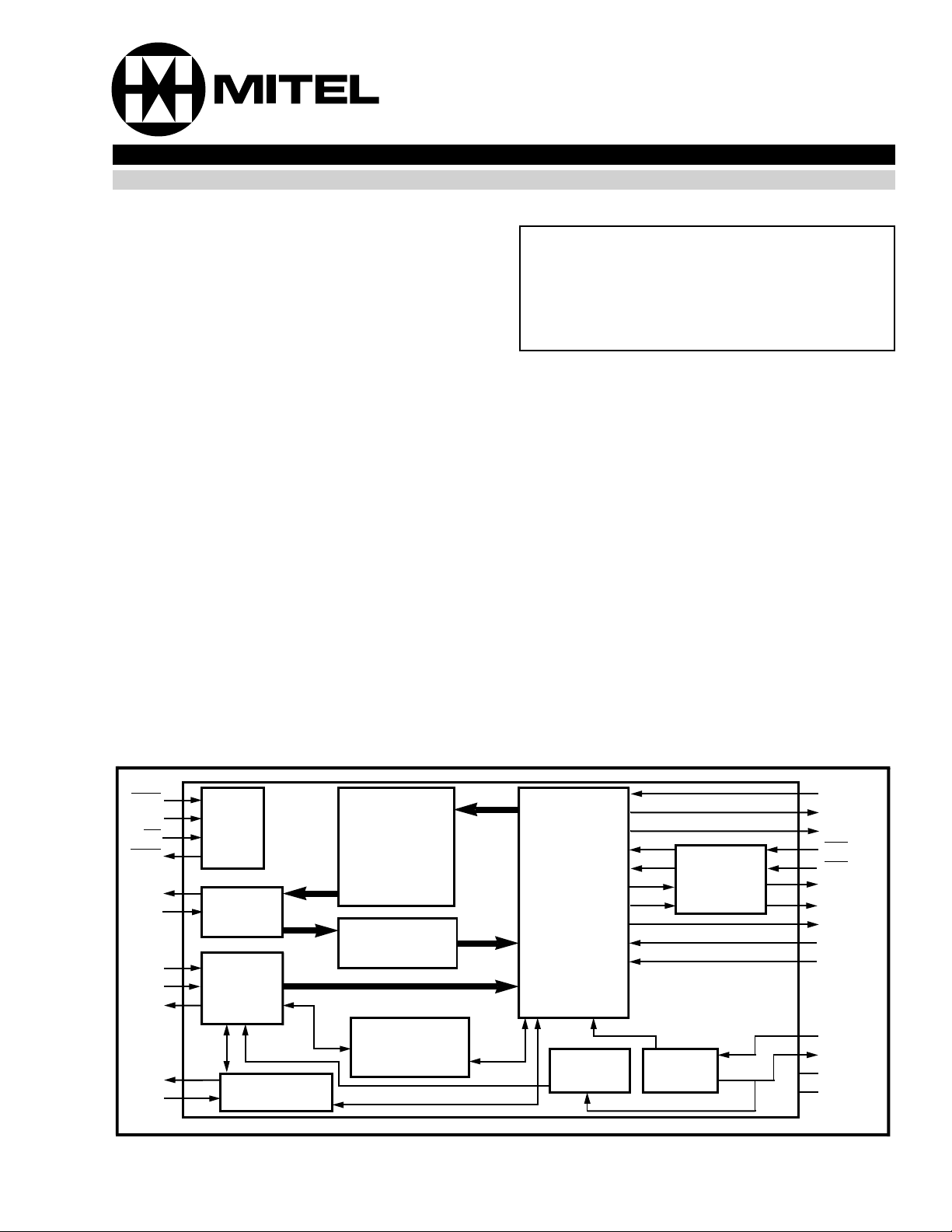
TxSF
C2i
F0i
RxSF
DSTo
DSTi
CSTi0
CSTi1
CSTo
XCtl
XSt
ST-BUS
Timing
Circuitr y
Data
Interface
Serial
Control
Interface
Control Logic
2 Frame
Elastic Buf fer
with Slip
Control
2048-1544
Converter
ABCD
Signalling RAM
Figure 1 - Functional Block Diagram
ACCUNET® T1.5 is a register ed tra de m ark o f AT & T
DS1
Link
Inte rface
Phase
Detect or
Remote &
DS1
Counter
Digital
Loopbacks
C1.5i
RxFDLClk
RxFDL
RxA
RxB
TxA
TxB
TxFDLClk
TxFDL
RxD
E1.5i
E8Ko
V
•
SS
V
DD
4-99
Page 2
MT8977 ISO-CMOS Preliminary Information
1
TxA
2
TxB
DSTo
RxD
CSTi1
TxFDL
TxFDLClk
CSTi0
E8Ko
VSS
3
4
NC
5
RxA
6
RxB
7
8
9
10
11
NC
12
13
14
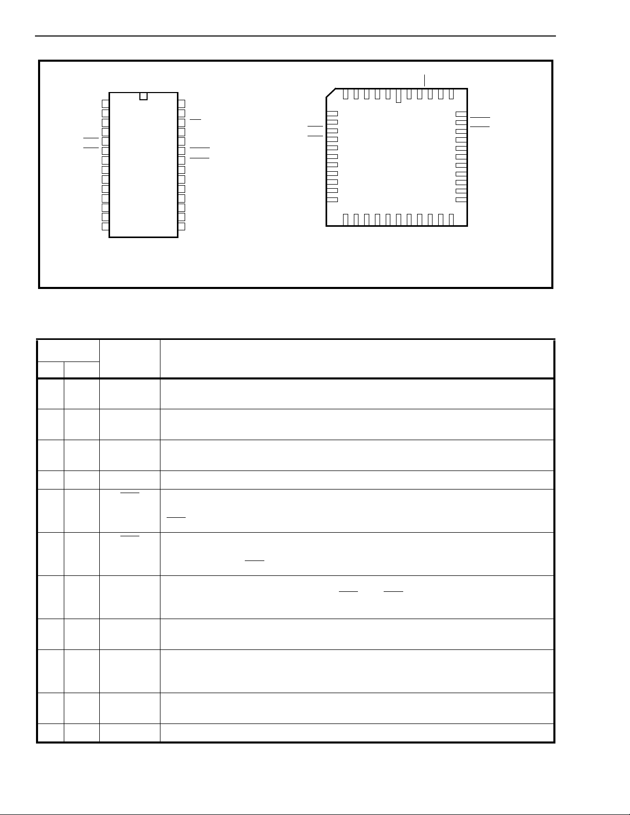
28 PIN CERDIP/PDIP
Pin Description
Pin #
DIP PLCC
Name Description
28
27
26
25
24
23
22
21
20
19
18
17
16
15
VDD
IC
F0i
E1.5i
C1.5i
RxSF
TxSF
C2i
RxFDL
DSTi
RxFDLClk
CSTo
XSt
XCtl
TxA
65432 44434241
7
NC
8
NC
NC
NC
NC
9
10
11
12
13
14
15
16
17
VSS
RxA
RxB
RxD
CSTi1
TxFDL
TxFDLClk
Figure 2 - Pin Conne ctions
TxBNCDSTo
NC
E8Ko
CSTi0
44 PIN PLCC
VDD
VSS
ICNCF0iNCE1.5i
1
2318192021 22 2425 262728
XCtl
VSS
DSTi
CSTo
RxFDLClk
40
39
38
37
36
35
34
33
32
31
30
29
NC
XSt
C1.5i
RxSF
TxSF
NC
NC
C2i
NC
NC
NC
NC
RxFDL
12 TxATransmit A Outpu t. Unipolar output that can be used in conjunction with TxB and
external line driver circuitry to generate the bipolar DS1 signal.
23 TxBTransmit B Output. Unipolar output that can be used in conjunction with TxA
and external line driver circuitry to generate the bipolar DS1 signal.
3 5 DSTo Data ST-BUS Output. A 2048 kbit/s serial output stream which contains the 24
PCM or data channels received from the DS1 line.
44 NC No Connection.
59 RxA
Receive A Complementary Input. Accepts a unipolar split phase signal decoded
externally from the received DS1 bipolar signal. This input, in conjunction with
, detects bipolar violations in the received signal.
RxB
610 RxB
Receive B Complementary Input. Accepts a unipolar split phase signal
decoded externally from the received DS1 bipolar signal. This input, in
conjunction with RxA
, detects bipolar violations in the received signal.
711 RxD Receive Data Input. Unipolar RZ data signal decoded from the received DS1
signal. Gener al l y the signals input at RxA
and RxB are combined externally with a
NAND gate and the resulting composite signal is input at this pin.
813 CSTi1Control ST-BUS Input #1. A 2048 kbit/s serial control stream which carries 24
per-channel control words.
9 14 TxFDL Transmit Facility Data Link (Input). A 4 kHz serial input stream that is
multiplexed into the FDL posit i on in the ESF mode, or the F
pattern when in SLC-
S
96 mode. It is clocked in on the rising edge of TxFDLClk.
10 16 TxFDLClk Transmit Fa cility Da ta Link Clock (O utput). A 4 kHz clock used to clock in the
FDL data.
11 NC No connection.
4-100
Page 3

Preliminary Information ISO-CMOS MT8977
Pin Description (Continued)
Pin #
Name Description
DIP PLCC
12 19 CSTi0 Control ST-BUS Input #0. A 2048 kbit/s serial control stream that contains 24 per
channel control words and two master control words.
13 20 E8Ko Extracted 8 kHz Output. The E1.5i clock is internally divided by 193 to produce an
8 kHz clock which is aligned with the received DS1 frame and output at this pin. The
8 kHz signal is derived from C1.5 in Digital Loopback mode.
14 6,
V
SS
System Ground.
18,
22
15 23 XCtl External Control (Output). This is an uncommitted external output pin which is set
or reset via bit 3 in Master Control Word 1 on CSTi0. The state of XCtl is updated
once per frame.
16 24 XSt External Status (Schmitt T rigger Input). The state of this pin is sampled once per
frame and the status is reporte d in bit 5 of Master Status Word 2 on CSTo .
17 26 CSTo Control ST-BUS Output. This is a 2048 kbit/s serial control stream which provides
the 24 per-channel status words, and two master status words.
18 27 RxFDLClk Receive Facility Data Link Clock (Output). A 4 kHz clock signal used to clock out
FDL information. The data is clocked out on the rising edge of RxFDLClk.
19 28 DSTi Data ST-BUS Input. This pin accepts a 2048 kbit/s serial stream which contains the
24 PCM or data channels to be transmitted on the T1 trunk.
20 29 RxFDL Received Facility Data Link (Output). A 4 kHz serial output stream that is
demultiplexed from the FDL in E SF mode, or the received Fs bit pattern in SLC-96
mode. It is clocked out on the rising edge of RxFDLClk.
21 34 C2i 2.048 MHz Clock Input. This is the master clock used for clocking serial data into
DSTi, CSTi0 and CSTi1. It is also used to clock serial data out of CSTo and DSTo.
22 37 TxSF
Transmit Superframe Pulse Input. A low going pulse applied at this pin will make
the next transmit frame the first frame of a superframe. The device will free run if
this pin is held high.
23 38 RxSF
Received Superframe Pulse Output. A pulse output on this pin designates that the
next frame of data on the ST-BUS is from frame 1 of the received superframe. The
period is 12 frames long in D3/D4 modes and 24 frames in ESF mode. Pulses are
output only when the device is synchronized to the received DS1 signal.
24 39 C1.5i 1.544 MHz Clock Input. This is the DS1 transmit clock and is used to output data on
TxA and TxB. It must be phase-locked to C2i. Data is clocked out on the rising
edge of C1.5i.
25 40 E1.5i 1.544 MHz Extracted Clock (Input). This clock which is extracted from the received
, RxB and RxD . The falling edge of the clock
and RxB.
26 42 F0i
data is used to clock in data at RxA
is nominally aligned with the cente r of the received bit on RxD, RxA
Frame Pulse Inpu t. This is the frame synchronization signal which defines the
beginning of the 32 channel ST-BUS frame.
27 44 IC Internal Connecti on. Tied to V
28 1 V
DD
Positive Pow er Su pp ly Inpu t. +5V ±5%.
for normal operation
SS
.
4-101
Page 4
MT8977 ISO-CMOS Preliminary Information
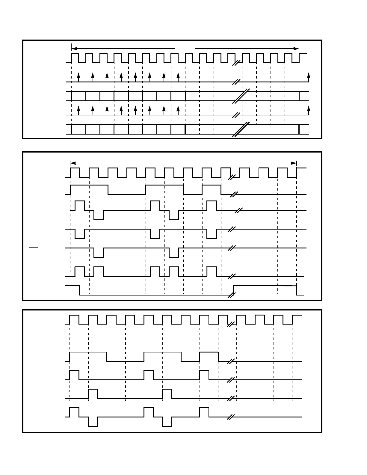
Functional Timing Diagrams
125µSec
C2i
DSTi
DSTo
CSTi0/CSTi1
CSTo
E1.5i
INT DATA
DS1 AMI
LINE SIGNAL
RxA
RxB
765 4
7
1
6
1
5
4
0
3
3
2
2
1
1
0
0
•
•
Figur e 3 - S T-BUS Ti ming
125µSec
01
10
•
•
1
•
•
•
•
•
•
•
•
•
•
7
•
7
•
RxD
E8Ko
C1.5i
INT DATA
TxA
TxB
DS1 AMI
LINE SIGNAL
Figur e 4 - D S1 Re ceiv e Ti mi ng
Figure 5 - DS1 Transm it Tim in g
4-102
Page 5

Preliminary Information ISO-CMOS MT8977
29 30 31
25 26 27 28
21 22 23 24
17 18 19 20
30
29
28
26
25
24
22
21
20
18
17
16
31
PC
PC
PC
27
PC
PC
PC
23
PC
PC
PC
19
PC
PC
PC
15
X
CW
CW
CW
X
CW
CW
CW
X
CW
CW
CW
X
CW
CW
CW
X
31
MS
W2
2
2
2
2
2
2
2
2
2
2
2
2
15
30
29
28
26
25
24
22
21
20
18
17
16
27
23
19
MS
W
PCS
W
PCS
W
PCS
X
W
PCS
W
PCS
W
PCS
X
W
PCS
W
PCS
W
PCS
X
W
PCS
W
PCS
W
PCS
W1
31
W2
MC
PC
PC
PC
27
PC
PC
PC
23
PC
PC
PC
19
PC
PC
PC
MC
CW
CW
CW
X
CW
CW
CW
X
CW
CW
CW
X
CW
CW
CW
W1
1
1
1
1
1
1
1
1
1
1
1
1
30
29 30 31
X
X
X
X
X
25 26 27 28
X
21 22 23 24
X
17 18 19 20
X
29
28
26
25
24
22
21
20
18
17
16
15
13 14 15 16
X
9 101112
X
5678
X
1234
X
ST-BUS CHANNEL VERSUS DS1 CHANNEL TRANSMITTED
13 14 15 16
X
9 101112
X
5678
X
1234
X
ST-BUS CHANNEL VERSUS DS1 CHANNEL RECEIVED
14
13
12
10
9
8
6
5
4
2
1
PC
PC
PC
11
PC
PC
PC
7
PC
PC
PC
3
PC
PC
PC
CW
CW
CW
X
CW
CW
CW
X
CW
CW
CW
X
CW
CW
CW
1
1
1
1
1
1
1
1
1
1
1
1
14
13
12
10
9
ST-BUS CHANNEL VERSUS DS1 CHANNEL CONTROLLED
8
6
5
4
3
2
1
PC
PC
PC
11
PC
PC
PC
7
PC
PC
PC
X
PC
PC
PC
CW
CW
CW
X
CW
CW
CW
X
CW
CW
CW
CW
CW
CW
2
2
2
2
2
2
2
2
2
2
2
2
ST-BUS CHANNEL VERSUS DS1 CHANNEL CONTROLLED
W
14
PCS
W
13
PCS
W
12
PCS
X
11
W
10
PCS
9
W
PCS
8
W
PCS
7
X
6
W
PCS
5
W
PCS
4
W
PCS
3
W
PS
2
W
PCS
1
W
PCS
W
PCS
Figure 6 - ST-BUS Channel Allocations
ST-BUS VERSUS DS1 CHANNEL STATUS
DSTi 0
DS1 1 2 3 4 5 6 7 8 9 10 11 12 13 14 15 16 17 18 19 20 21 22 23 24
DSTo 0
DS1 1 2 3 4 5 6 7 8 9 10 11 12 13 14 15 16 17 18 19 20 21 22 23 24
CSTi0 0
DS1 1 2 3 4 5 6 7 8 9 10 11 12 13 14 15 16 17 18 19 20 21 22 23 24
PCCW = Per Channel Control Word
MCW1/2 =Ma ster Cont rol Word 1 /2
CSTi1 0
DS1 1 2 3 4 5 6 7 8 9 10 11 12 13 14 15 16 17 18 19 20 21 22 23 24
PCCW = Per Channel Control Word
CSTo 0
DS1 1 2 3 4 5 6 7 8 9 10 11 12 13 14 15 16 17 18 19 20 21 22 23 24
X = Unused
PCSW =Per C hann el St atus Word
PSW = Phase Sta tus Wo rd
MSW =M aster Status Word
4-103
Page 6

MT8977 ISO-CMOS Preliminary Info rm atio n
Functional Description
The MT8977 provides a simple interface to a
bidirectional DS1 link. All of the formatting and
signalling insertion and detection is done by the
device. Various programmable options in the device
include: ESF, D3/D4, or SLC-96 mode, common
channel or robbed bit signalling, zero code
suppression, alarms, and local and remote loop
back. All data and control information is
communicated to the MT8977 via 2048 kbit/s serial
streams co nf or mi n g to Mite l ’s ST-BUS fo rma t.
The ST-BUS is a TDM serial bus that operates at
2048 kbits/s. The serial streams are divided into 125
µsec frames that are made up of 32 8 bit channels.
A serial stream that is made up of these 32 8 bit
channels is known as an ST-BUS stream, and one of
these 64 kbit/s channels is known as an ST-BUS
channel.
The system side of the MT8977 is made up of STBUS inputs and outputs, i.e. control inputs and
outputs (CSTi/o) and data inputs and outputs
(DSTi/ o). These signals are functionally represented
in Figure 3. The line side of the device is made up of
the split phase inputs and outputs that can be
interfaced to an external bipolar receiver and
transmitter. Functional transmit and receive
timing is shown in Figures 4 and 5.
Data for transmission on the DS1 line is clocked
serially into the device at the DSTi pin. The DSTi pin
accepts a 32 channel time division multiplexed STBUS stre a m . Data is cl o c ked i n w i th th e fa l ling edge
of the C2i clock. ST-BUS frame boundaries are
defined by the frame pulse applied at the F0i pin.
Only 24 of the available 32 channels on the ST-BUS
serial stream are actually transmitted on the DS1
side. The unused 8 channels are ignored by the
device.
Data recei ved from the DS1 li ne i s cl o c ke d o ut of th e
device in a similar manner at the DSTo pin. Data is
clocked out on the rising edge of the C2i clock. Only
24 of the 32 channels output by the device contain
the information from the DS1 line. The DSTo pin is,
however, actively driven during the unused channel
timeslots. Figure 6 shows the correspondence
between the DS1 channels and the ST-BUS
channels.
All control and monitoring of the device is
accomplished through two ST-BUS serial control
inputs and one serial control output. Cont rol ST-BUS
input number 0 (CSTi0) accepts an ST-BUS serial
stream which contains the 24 per channel control
words and two master control words. The per
channel control words relate directly to the 24
information channels output on the DS1 side. The
master control words affect operation of the whole
device. Control ST-BUS input number 1 (CSTi1)
accepts an ST-BUS stream containing the A, B, C
and D signalling bits. The relationship between the
CSTi channels and the controlled DS0 channels is
shown in Figure 6. Status and signalling information
is received from the device via the control ST-BUS
output (CSTo). This serial output stream contains
two master status words, 24 per channel status
words and one Phase Status Word. Figure 6 shows
the correspondence between the received DS1
channels and the status words. Detailed information
on the operation of the control interface is presented
below.
Progra m ma ble Fe atu res
The main features in the device are programmed
through two master control words which occupy
channels 15 and 31 in Control ST-BUS input stream
number 0 (CSTi0). These two eight bit words are
used to:
• Select the different operating modes of the
device ESF, D3/D4 or SLC-96.
• Activate t he fe atur es tha t are ne eded i n a
certain application; common channel signalling,
zero code s uppre ssi on, si gnall ing de bounc e,
etc.
• Turn on in service alarm s, di agnos tic loop
arounds, an d the extern al c ontrol fun ction .
Tables 1 and 2 contain a complete explanation of
the function of the different bits in Master Control
Words 1 and 2.
Major Operating Modes
The major operating modes of the device are
enabled by bits 2 and 4 of Master Control Word 2.
The Extended Superframe (ESF) mode is enabled
when bit 4 is set high. Bit 2 has no effect in this
mode. The ESF mode enables the transmission of
the S bit pattern shown in Table 3. This includes the
frame/superframe pattern, the CRC-6, and the
Facility Data Link (FDL). The device generates the
frame/multiframe pattern and calculates the CRC for
each superframe. The data clocked into the device
on the TxFDL pin is incorporat ed into the FDL. ESF
mode will also insert A, B, C and D signalling bits into
the 24 frame multiframe. The DS1 frame begins
after approximately 25 periods of the C1.5i clock
from the F0i
During synchronization the receiver locks to the
incoming frame, calculates the CRC and compares it
frame pulse.
4-104
Page 7

Preliminary Information ISO-CMOS MT8977
Bit Name Description
7 Debounce When set the received A, B, C and D signalling bits are reported directly in the per channel status
words output at CSTo. When clear, the signalling bits are debounced for 6 to 9 ms before they are
placed on CSTo.
6 TSPZCS Transparent Zero Code Suppression. When this bit is set, no zero code suppression is
implemented.
5 B 8ZS Binary Eight Zero Suppression. When this bit is set, B8ZS zero code suppression is enabled.
When clear, bit 7 in data channels containing all zeros is forced high before being transmitted on the
DS1 side. This bit is inactive if the TSPZCS bit is set.
4 8KHSel 8 kHz Output Select. When set, the E8Ko pin is held high. When clear, the E8Ko generates an 8
kHz output derived from the E1.5i or C1.5 clock (see Pin Description for E8Ko).
3 XCtl External Control Pin. When set, the XCtl pin is held high. When clear, XCtl is held low.
2 ESFYL W ESF Yellow Alarm. V alid only in ESF mode. When set, a sequence of eight 1’s followed by eight 0’s
is sent in the FDL bit positions. When clear, the FDL bit contains data input at the TxFDL pin.
1 Robbed bit When this bit is set, robbed bit signalling is disabled on all DS0 transmit channels. When clear, A, B,
C and D signalling bit insertion in bit 8 for all DS0 transmit channels in every 6
0 YLALR Yellow Alarm. When set, bit 2 of all DS1 channels is set low. When clear, bit 2 operates normally.
Table 1. Master Control Word 1 (Channel 15, CSTi0)
th
frame is enabled.
.
to the CRC received in the next multiframe. The
device will not declare itself to b e in s ynchro n ization
unless a valid framing pattern in the S-bit is detected
and a correct CRC is received. The CRC check in
this case provides protection against false framing.
The CRC check can be turned off by setting bit 1 in
Master Control Word 2.
The device can be forced to r esynchronize itself. If
Bit 3 in Master Contr ol Word 2 is set for one frame
and then sub sequently reset, the d evice will start to
search for a new frame position. The decision to
reframe is made by the user’s system processor on
the basis of the status conditions detected in the
received master status words. This may include
consideration of the number of errors in the received
CRC in conjunction with an indication of the presence
of a mimic. Wh en the devi ce attain s sy nchroniza tion
the mimic bit in Master Status Word 1 is set if the
device found anothe r poss ible can didate w hen it was
searching for the fram i ng pa tter n.
Note that the device will resynchronize automatically
if the errors in the terminal framing pattern (F
T
or
FPS) exceed the threshold set with bit 0 in Master
Control Word 2.
Standard D3/D4 framing is enabled when bit 4 of
Master Control Word 2 is reset (logic 0). In this
mode the device searches for and inserts the
framing pattern shown in Table 4. This mode only
supports AB bit signalling, and does not contain a
CRC check.
The CRC/MIMIC bit in Master Control Word 2, when
set high, allows the device to synchronize in the
presence of a mimic. If this bit is reset, the device
will not synchronize in the presence of a mimic (Also,
refer to section on Framing algorithm).
In the D3/D4 mode the device can also be made
compatible with SLC-96 by setting bit two of Master
Control Word 2. This allows the user to insert and
extract the signalling framing pattern on the DS1 bit
stream using the FDL input and output pins. The user
must format this 4 kbits of information externally to
meet all of the requirements of the SLC-96
specification (see Table 5). The device multiplexes
and demultiplexes this information into the proper
position. Thi s mo de of operation c an also be used for
any other application that uses all or part of the
signalling framing pattern. As long as the serial
stream clocked into the TxFDL contains two proper
sets of consecutive synchronization bits (a s shown in
Table 5 for frames 1 to 24), the device will be able to
insert and extract the A, B signalling bits. The TxSF
pin should be held high in this mode. Superframe
boundaries cannot be defined by a pulse on this
input. The RxSF
output functions normally and
indicates the superframe boundaries based on the
synchronization pattern in the F
received bit
S
position.
Zero Code Suppression
The combination of bits 5 and 6 in Master Control
Word 1 allow one of three zero code suppression
schemes to be selected. The three choices are:
none, binary 8 zero suppression (B8ZS), or jammed
bit (bit 7 forced high). No zero code suppression
4-105
Page 8

MT8977 ISO-CMOS Preliminary Information
Bit Name Description
7 RMLOOP Remote Loopback. When set, the data received at RxA and RxB is looped back to TxB and T xA
respectively. The data is clocked into the device with E1.5i. The device still monitors t he received
data and outputs it at DSTo. The device operates normally when the bit is clear.
6 DGLOOP Digital Loopback. When set, the data input on DSTi is looped around to DSTo. The normal received
data on RxA
and TxB. The device frames up on the looped data using the C1.5i clock.
5 ALL1'S All One’s Alarm. When set, the chip transmits an unframed all 1's signal on TxA and TxB.
4 ESF/D4 ESF/D4 Select. When set, the device is in ESF mode. When clear, the device is in D3/D4 mode.
3 ReFR Reframe. If set for at least one frame and then cleared, the chip will begin to search for a new frame
position. Only the change from high to low will cause a reframe, not a continuous low level.
2 SLC-96 SLC-96 Mode Select. The chip is in SLC-96 mode when this bit is set. This enables input and
output of the F
use the same framing algorithm as D3/D4 mode. The user must insert the valid F
superframes to allow the receiver to find superframe sync, and the transmitter to insert A and B bits
in eve ry 6
Inactive in ESF mo de.
1 CRC/MIMIC In ESF mode, when set, the chip disregards the CRC calculation during synchronization. When
clear, the device will check for a correct CRC before going into synchronization. In D3/D4 mode,
when set, the device will synchronize on the f irst c orrect S-bit pattern detected. When this bit is
clear, the device will not synchronize if it has detected more than one candidate for the frame
alignment pattern (i.e., a mimic).
0 Maint. Maintenance Mode. When set, the device will declare itself out-of-sync if 4 out of 12 c onsecutive F
bits are in error. When clear, the out-of-sync threshold is 2 errors in 4 F
consecutive bits following an errored F
, RxB and RxD is ignored. However, the data input at DSTi is still transmitted on TxA
bit pattern using the same pins as the facility data link in ESF mode. The chip will
S
th
frame. The SLC-96 FDL completely replaces the FS pattern in the outgoing S bit position.
bits. In this mode, four
bit are examined.
T
T
bits in 2 out of 6
S
T
.
Table 2. Master Control Word 2 (Channel 31, CSTi0)
allows the device to interface with systems that have
already applied some form of zero code suppression
to the data input on DSTi. B8ZS zero code
suppression replaces all strings of 8 zeros with a
known bit pattern and a specific pattern of bipolar
violations. This bit pattern and violation pattern is
shown in Figure 7. The receiver monitors the
received bit pattern and the bipolar violation pat tern
and replaces all matching strings with 8 zeros.
Loopback Modes
Remote and digital loopback modes are enabled by
bits 6 and 7 i n M a ster C on tro l Wo rd 2 . These mo des
can be us ed for diagnostics in locating the source of a
fault condition. Remote loop around loops back data
received at RxA
and RxB back out on TxA and TxB,
thus effectively sending the received DS1 data back
to the far e nd unalte red so th at the tra nsmission l ine
can be tested. The received signal is still monitored
with the appropriate received channels on the DS1
side made available in the proper format at DSTo.
no transmission line or when there is a suspected
failure of the line.
The all one’s transmit alarm (also known as the blue
alarm or the keep alive signal) can be activated in
conjunction with the digital loop around so that the
transmission line sends an all 1's signal while the
normal data is looped back locally.
The MT8977 also has a per channel loopback mode.
See Table 6 and the following section for more
information.
Per Channel Control Features
In addition to the two master control words in C STi0
there are a lso 24 Per Chan nel Co ntrol Words. T hes e
control words only affect individual DS0 channels.
The correspondence between the channels on CSTi0
and the affected DS0 channel is shown in Fig. 6.
The digital loop around mode diverts the data
received at DSTi back out the DSTo pin. Data
received on DSTi is, however, still transmitted out via
TxA and TxB. This loop back mode can be used to
test the near end interface equipment when there is
4-106
Page 9

Preliminary Information ISO-CMOS MT8977
ABCD signalling bits is shown in Table 7. Even
Frame # FPS FDL CRC Signalling
1X
2CB1
3X
40
5X
6 CB2 A
7X
80
9X
10 CB3
11 X
12 1 B
13 X
14 CB4
15 X
16 0
17 X
18 CB5 C
19 X
20 1
21 X
22 CB6
23 X
24 1 D
†
Table 3. ESF Frame Pattern
† T hese signalli ng bits are only valid if the robbed bit signal li ng is
active.
though the device only inserts the signalling
information in every 6th DS1 frame this information
must be input every ST-BUS frame.
Robbed bit signalling can be disabled for all
channels on the DS1 link by bit 1 of Master Control
Word 1. It can also be disabled on a per channel
basis by bit 0 in the Per Channel Control Word 1.
Operatin g Stat us Inf ormat ion
Status Information regarding the operation of the
device is output serially via the Control ST-BUS
output (CSTo). The CSTo serial stream contains
Master Status Words 1 and 2, 24 Per Channel Status
Words, and a Phase Status Word. The Master
Status Words contain all of the information needed to
determine the state of the interface and how well it is
operating. The information provided includes frame
and super frame synchronization, slip, bipolar
violation counter, alarms, CRC error count, F
error
T
count, synchronization pattern mimic and a phase
status word. Tables 8 and 9 give a description of
each of the bits in Master Status Words 1 and 2, and
Table 10 gives a description of the Phase Status
Word.
Frame # F
11
20
30
40
51
61A
70
81
91
10 1
11 0
12 0 B
T
F
S
Signalling
†
Table 4. D3/D4 Framer
† T hese signalli ng bits are only valid if the robbed bit signal li ng is
active.
Each control word has three bits that enable robbed
bit signalling, DS0 channel loopback and inversion of
the DS0 channel. A full description of each of the
bits is provided in Table 6.
Transmit Signalling Bits
Control ST-BUS input number 1 (CSTi1) contains 24
additional per channel control words. These 24 STBUS channels contain the A, B, C and D signalling
bits that the device uses at transmit time. The
position of these 24 per channel control words in the
ST-BUS is
shown in Figure 6 and the position of the
Alarm Detectio n
The device detects the yellow alarm for both D3/D4
frame format and ESF format. The D3/D4 yellow
alarm will be activated if a ‘0‘ is received in bit
position 2 of every DS0 channel for 600 msec. It will
be released in 200 msec after the contents of the bit
change. The alarm is detectable in the presence of
errors on the line. The ESF yellow alarm will
become active when the device has detected a string
of eight 0’s followed by eight 1’s in the facility data
link. It is not detectable in the presence of errors on
the line. This means that the ESF yellow alarm will
drop out for relatively short periods of time, so the
system will have to integrate the ESF yellow alarm.
The blue alarm signal, in Master Status Word 2, will
also drop out if there are errors on the line.
Mimic De te cti on
The mimic bit in Master Status Word 1 will be set if,
during synchronization, a frame alignment pattern
or FPS bit pattern) was observed in more than
(F
T
one position, i.e., if more than one candidat e for the
frame synchronization position was observed. It will
be reset when the device resynchronizes. The
mimic bit, the terminal framing error bit and the CRC
error counter can be used separately or together to
decide if t he r e ce ive r sh o uld b e fo r c ed to re fr a me .
4-107
Page 10

MT8977 ISO-CMOS Preliminary Information
A
A
A
A
A
A
A
Frame
#
F
T
11
†
F
S
Notes
Frame
#
37 1
F
T
†
F
S
20 38X
30 390
40 40X
51 411
60 42X
70 430
81 44X
91 451
10 1 46 X
11 0 47 0
12 1 48 S
13 1 49 1
14 0 50 S
Resynchronization
Data
Bits
15 0 51 0
16 0 52 S
17 1 53 1
18 0 54 C
19 0 55 0
20 1 56 C
21 1 57 1
22 1 58 C
23 0 59 0
24 1 60 A
25 1
61 1
26 X 62 A
27 0 63 0
28 X 64 L
29 1 65 1
30 X 66 L
31 0 67 0
X = Concentrator
Field Bits
32 X 68 L
33 1 69 1
34 X 70 L
35 0 71 0
36 X 72 S
Table 5. SLC-96 Framing Pattern
† Note: The FS pattern has to be supplied by the user
Notes
X = Concentrator
Field Bits
S = Spoiler Bits
C = Maintenance
Field
Bits
A = Alarm Field
Bits
L = Line Switch
Field Bits
S = Spoiler Bits
DATA
B8ZS
B8ZS
BV
B
0
0
0
0
0
B
0
V
B
0
V
V
0
B
B
B
B
V = Violation
B = Bipolar
0 = No Pulse
Figure 7 - B8ZS Output Coding
4-108
Page 11

Preliminary Information ISO-CMOS MT8977
Bipolar Violation Counter
The Bipolar Violation bit in Master Status Word 1 will
toggle after 256 violations have been detected in the
received signal. It has a maximum refresh time of 96
ms. This means that the bit can not change state
faster than once every 96 ms. For example, if there
are 256 violations in 80 ms the BPV bit will not
change state until 96 ms. Any more errors in that
extra 16 ms are not counted. If there are 256 errors
in 200 ms then the BPV bit will change state after
200 ms. In practical terms this puts an upper limit on
the error rate that can be calculated from the BPV
information, but this rate (1.7 X 10
-3
) is well above
any normal operating condition.
Bits 4 and 3 also provide bipolar violations information. Bit 4 will change state after 128 violations.
Bit 3 changes state after 64 bipolar vi olations. These
bits are refreshed independently and are not subject
to the 96 ms refresh rate described above.
DS1/ST-BUS Phase Difference
An indication of the phase difference between the
ST-BUS and the DS1 frame can be ascertained from
the information provided by the eight bit Phase
Status Word and the Frame Count bit. Channel
three on CSTo contains the Phase Status Word. Bits
7-3 in this word indicate the number of ST-BUS
channels between the ST-BUS frame pulse and the
rising edge of the E8Ko signal. The remaining three
bits provide one bit resolution within the channel
count indicated by bits 7-3. The frame count bit in
Master Status Word 2 is the ninth and most
significant bit of the phase status word. It will toggle
when the phase status word increments above
channel 31, bit 7 or decrements below channel 0, bit
0. The E8Ko signal has a specific relationship with
received DS1 frame. The rising edge of E8Ko
occurs during bit 2, channel 17 of the received DS1
frame. The Phase Status Word in conjunction with
the frame count bit, can be used to monitor the
phase relationship between the received DS1 frame
and the local ST-BUS frame.
The local 2.048 MHz ST-BUS clock must be phaselocked to the 1.544 MHz clock extracted from the
received data. When the two clocks are not phaselocked, the input data rate on the DS1 side will differ
from the output data rate on the ST-B US side. If the
average input data rate is higher than the average
output data rate, the channel count and bit count in
the phase status word will be seen t o decrease over
time, indicating that the E8Ko rising edge, and
therefore, the DS1 frame boundary is moving with
respect to the ST-BUS frame pulse. Conversely, a
lower average input data rate will result in an
increase in the phase reading.
In an application where it is necessary to minimize
jitter transfer from the received clock to the local
system clock, a phase lock loop with a relatively
large time constant can be implemented using
information provided by the phase status word. In
such a system, the local 2.048 MHz clock is derived
from a precision VCO. Frequency corrections are
made on the basis of the average trend observed in
the phase status word. For example, if the channel
count in the phase status word is seen to increase
over time, the feedback applied to the VCO is used
to decrease the system clock frequency until a
reversal in the trend is observed.
Bit Name Description
7-3 IC Internal Connections. Must be kept at 0 for normal operation
2 Polarity When set, the applicable channel is not inverted on the transmit or the receive side of the device.
When clear, all the bits within the applicable channel are inverted both on transmit and receive
side.
1 Loop Per Channel Loopback. When set, the received DS0 channel is replaced with the transmitted
DS0 channel. Only one DS0 channel may be looped back in this manner at a time. The
transmitted DS0 channel remains unaffected. When clear the transmit and receive DS0 sections
operate normally.
0 Data Data Channel Enable. When set, robbed bit signalling for the applicable channel is disabled.
When clear, every 6th DS1 frame is available for robbed bit signalling. This feature is enabled
only if bit 1 in Master Control Word is low.
Table 6. Per Channel Control Word 1 Input at CSTi0
Bit Name Description
7-4 Unused Keep at 0 for normal operation
3
2
1-0
A
B
C, D
These are the 4 signalling bits inserted in the appropriate channels of the DS1 stream being
output from the chip, when in ESF mode. In D3/D4 modes where there are only t wo signalling
bits, the values of C and D are ignored.
Table 7. Per Channel Control Word 2 Input at CSTi1
4-109
Page 12

MT8977 ISO-CMOS Preliminary Information
Bit Name Description
7 YLALR Yellow Alarm Indicat ion. This bit is set when the chip is receiving a 0 in bit position 2 of every
DS0 channel.
6 M IMIC This bit is set if the frame search algorithm found more than one possible frame candidate when it
went into frame synchronization.
5 ERR Terminal Framing Bit Error. The state of this bit changes every time the chip detects 4 errors in
the F
or FPS bit pattern. The bit will not change state more than once every 96ms.
T
4 ESFYLW ESF Yellow Alarm. This bit is set when the device has observed a sequence of eight one’s and
eight 0’s in the FDL bit positions.
3
2 BPV Bipolar Violation Count. The state of this bit changes every time the device counts 256 bipolar
1 SLIP Slip Indication. This bit changes state every time the elastic buff er in the device performs a
0
MFSYNC
SYN
Bit Name Description
7 BlAlm Blue Alarm. This bit is set if the receiver has detected two frames of 1’s and an out of frame
6 FrCnt Frame Count. This is the ninth and most significant bit of the “Phase Status Word“ (see Table
5 XSt External Status. This bit reflects the state of the external status pin (XSt). The state of the XSt
4-3 BPVCnt Bipolar Violation Count. These two bits chang e state ev ery 128 and every 64 bipolar violations,
2-0 CRCCNT CRC Error Count. These three bits count received CRC errors. The counter will reset to zero
Multiframe Synchronization. This bit is cleared when D3/D4 multiframe synchronization has
been achieved. Applicable only in D3/D4 and SLC-96 modes.
violations.
controlled slip.
Synchronization. This bit is set when the device has not achieved synchronization. The bit is
clear when the device has synchronized to the received DS1 data stream.
Table 8. Master Status Wor d 1 (Ch annel 15, CSTo)
condition. It is reset by any 250 microsecond interval that contains a zero.
10). If the phase status word is incrementing, this bit will toggle when the phase reading exceeds
channel 31, bit 7. If the phase word is decrementing, then this bit will toggle when the reading
goes below channel 0, bit 0.
pin is sampled once per frame.
respectively.
when it reaches terminal count. Valid only in ESF mode.
Table 9. Master Status Wor d 2 (Ch annel 31, CSTo)
Bit Name Description
7-3 ChannelCnt Channel Count. These five bits indicate the ST-BUS channel count between the ST -BUS frame
pulse and the rising edge of E8Ko.
2-0 BitCnt Bit Count. These three bits provide one bit resolution within the channel count described above.
Table 10. Phas e Sta tus Word (Cha nnel 3, CS To)
Bit N am e Description
7-4 Unused Unused Bits. Will be output as 0’s.
3
2
1
0
A
B
C
D
These are the 4 signalling bits as extracted from the received DS1 bit stream.
The bits are debounced for 6 to 9 ms i f th e d ebounc e feature is enabled via bit 7 in Master Control
Word 1.
Table 11. Per Channel Status Word Output on CSTo
The elastic buffer in the MT8977 permits the device
to handle 26 ST-BUS channels or 156 UI of jitter/
wander (see description of elastic buffer in the next
jitter/wander to be handled. However, for most
applications, including ACCUNET
®
T1.5 (138 UI),
the 156 UI of jitter/wander tolerance is acceptable.
section). In order to prevent slips from occurring, the
frequency corrections would have t o be implemented
such that the deviation in the phase status word is
limited to 26 channels peak-to-peak. It is possible to
use a more sophisticated protocol, which would
center the elastic buffer and permit more
4-110
Page 13

Preliminary Information ISO-CMOS MT8977
Received Signalling Bits
The A, B, C and D signalling bits are output from the
device in the 24 Per Channel Status Words. Their
location in the serial steam output at CSTo is shown
in Figure 6 and the bit positions are shown in Table
11. The internal debouncing of the signalling bits
can be tur ned o n or off by Ma ster Contro l Wo rd 1 . In
ESF mode, A, B, C and D bits are valid. Even
though the signalling bits are only received once
every six frames the device stores the information so
that it is available on the ST-BUS every frame. The
ST-BUS will always contain the most recent
signalling bits. The state of the signalling bits is
frozen if synchronization is lost.
In D3/D4 mode, only the A and B bits are valid. The
state of the signalling bits is frozen when terminal
frame synchronization is lost. The freeze is disabled
when the device regains terminal frame
synchronization. The signalling bits may go through
a random transition stage until the device attains
multifram e synchro nization .
Clock and Framing Signals
The MT8977 requires one 2.048 MHz clock (C2i) and
an 8 kHz framing signal for the ST-BUS side. Figure
2 illustrates the relationship between the two signals.
The framing signal is used to delimit individual 32
channel ST-BUS frames.
The DS1 side requires two clocks. A 1.544 MHz
clock used for transmit (C1.5i), and a 1.544 MHz
clock extracted from the DS1 line signal and applied
at E1.5i pin to clock in the received data.
The C2i and C1.5i clock must be phase-locked
together. There must be 193 clock cycles of C1.5i
for every 256 clock cycles of C2i. At the slave end of
the link, the C2i and C1.5i must be phase locked to
the extracte d E1 .5 i clo ck.
The clock applied at E1.5i is internally divided down
by 193 and aligned with the DS1 frame. The
resulting 8 kHz clock is output at the E8Ko pin. This
signal can be used as a reference for phase locking
the C2i and C1.5i clocks to the extracted 1.544 MHz
clock.
DS1 Line Interface
Transmit Interface
The interface to the DS1 line is made up of two
unipolar outputs, TxA and TxB, which can be used to
drive a bipolar transmitter circuit. The output signal
on TxA and TxB corresponds to the positive and
negative bipolar pulses required for the Alternate
Mark Inversion signal on the T1 line. The
relationship between the signal output at TxA and
TxB and the AMI signal is illustrated in Figure 5. For
transmission over twisted pair wire, the AMI signal
has to be equalized and transformer coupled to the
line.
Receiver Interface
The receiver circuitry is made up of three pins RxA
RxB
and RxD. The bipolar alternate mark inversion
signal from the DS-1 line should be converted into a
unipolar split phase format. The resulting signals
are clocked into the device at RxA
signals are also NANDED together and inp ut at RxD.
In special applications where the detection of bipolar
violation s is not r equi red, i t is pos sible to cloc k N RZ
data directly into RxD. In this case, the RxA
RxB
pins should be tied high.
Data is clocked into RxA
the falling edge of the E1.5i clock. This clock signal
is extracted from the received data. The relationship
between the received signals and the extracted clock
is shown in Figure 4.
Elastic Buffer
The MT8977 has a two frame elastic buffer which
absorbs jitter in the received DS1 signal. The buffer
is also used in the rate conversion between the
1.544 Mbit/s DS1 rate and the 2.048 Mbit/s ST-BUS
data rate .
The received data is written into the elastic buffer
with the extracted 1.544 MHz clock. The data is read
out of the buffer on the ST-BUS side with the system
2.048 MHz clock. The maximum delay through the
buffer is 1.875 ST-BUS frames or 60 ST-BUS
channels, see Figure 8. The minimum delay
required to avoid bus contention in the buffer
memory is two ST-BUS channels.
Under normal operating conditions, the system C2i
clock is phase locked to the extracted E1.5i clock
using external circuitry. If the two clocks are not
phase-locked, then the rate at which the data is
being written into the device on the DS1 side may
differ from the rate at which it is being read out on
the ST-BUS side. The buffer circuit will perform a
controlled slip if the throughput delay conditions
described above are violated. For example, if the
data on the DS1 side is being written in at a rate
slower than what it is being read out on the ST-BUS
side, the delay between the received DS1 write
pointer and the ST-BUS read pointer will begin to
, RxB and RxD with
and RxB. The
and
,
4-111
Page 14

MT8977 ISO-CMOS Preliminary Information
Write
Pointer
13 CH
47 CH
60 CH
386 Bit
Elastic
Store
34 CH
2 CH
15 CH
28 CH
Figure 8 - Elastic Bu ffer F unction al Dia gram (156 U I Wander Tolerance)
decrease over time. When this delay approaches
the minimum two channel threshold, the buffer will
perform a controlled slip, which will reset the in ternal
ST-BUS read pointers so that there is exactly 34
channels delay between the two pointers. This will
result in some ST-BUS channels containing
information output in the previous frame. Repetition
of up to one DS1 frame of information is possible.
Wander Tolerance
-13 CH
There is no loss of frame sync, multiframe sync or
any errors in the signalling bits when the device
performs a slip. The information on the FDL pins in
ESF or SLC-96 mode will, however, undergo slips at
the same time.
Framing Algorithm
Conversely, if the data on the DS1 side is being
written into the buffer at a rate faster than it is being
read out on the ST-BUS side, the delay between the
DS1 frame and the ST-BUS frame will increase over
time. A controlled slip will be performed when the
throughput delay exceeds 60 ST-BUS channels.
This slip will reset the internal ST-BUS counters so
that there is a 28 channel delay between the DS1
write pointer and the ST-BUS read pointer, resulting
in loss of up to one frame of received DS1 data.
Figure 8 illustrates the relationship between the read
and write pointers of the receive elastic buffer.
Measuring clockwise from the write pointer, if the
read point er comes within two channels of the writer
pointer a fra me slip w ill o ccur, which will pu t the read
pointer 34 channels from the write pointer.
Conversely, if the read pointer moves more than 60
channels from the write pointer, a slip will occur,
which will put the read pointer 28 channels from the
write pointer. This provides a worst case hysteresis
of 13 ST-BUS channels peak (26 ST-BUS channels
peak-to-peak). This can be translated into a low
frequency jitter (wander) tolerance value, accounting
for the DS1 to ST-BUS rate conversion, as follows:
(1.544/2.048) X 26 X 8 = 156 UI pp.
In ESF mode, the framer searches for a correct FPS
pattern. Figure 9 shows a state diagram of the
framing algorithm. The dotted lines show which
feature can be switched in and out depending upon
the operating mode of the device.
When the device is operating in the D3/D4 format,
the framer searches for the F
pattern, i.e., a
T
repeating 1010... pattern in a specific bit position
every alternate frame. It will synchronize to this
pattern and declare valid terminal frame
synchronization by clearing bit 0 in Master Status
Word 1. The device will subsequently initiate a
search for the F
frames (see Table 4). When a correct F
pattern to locate the signalling
S
pattern h a s
S
been located, bit 3 in Master Status Word 1 is
cleared indicating that the device has achieved
multiframe synchronization.
Note: the device will remain in terminal frame
synchronization even if no F
pattern can be loc ated.
S
In D3/D4 format, when the CRC/MIMIC bit in Master
Control Word 1 is cleared, the device will not go into
synchronization if more than one bit position in the
frame has a repeating 1010.... pattern, i.e., if more
than one candidate for the terminal framing position
is located. The framer will continue to search until
only one terminal framing pattern candidate is
4-112
Page 15

Preliminary Information ISO-CMOS MT8977
False Candidate
Hunt Mode
Candidate
Candidate
* Note: Only when in ESF mode and CRC
option is enabled.
Candidate
Verify
In sync
New Frame Position
False
Candidate
CRC
Check
Candidate
Vali d Ca n didate
False
Candidate
*
Resync
Receive r
Out of
Sync.
Forced
Reframe
Maintenance
Valid Ca ndidate
Figure 9 - Off-L ine Fr amer Sta te Diagr am
discovered. It is, therefore, possible that the device
may not synchronize at all in the presence of PCM
code sequences (e.g., sequences generated by
some types of test signals), which contain mimics of
the termina l fr am i ng p a tte r n.
Setting CRC/MIMIC bit high will force the framer to
synchronize to the first terminal framing pattern
detected. In standard D3/D4 applications, the user’s
system software should monitor the multiframe
synchronization state indicated by bit 3 in Master
Status Word 1. Failure of the device to achieve
multiframe synchronization within 4.5ms of terminal
frame synchronization, is an indication that the
device has framed up to a terminal framing pattern
mimic and should be forced to reframe.
One of the main features of the framer is that it
performs its function "off line". That is, the framer
repositions the receive circuit only when it has
detected a valid frame position. When the framer
exits maintenance mode the receive counters remain
where they are until the framer has found a new
frame position. This means that if the user forces a
reframe when the device was really in the right
place, there will not be any disturbance in the c ircuit
because the framer has no effect on the receiver
until it has found synchronization.
The out of
synchronization criterion can be controlled by bit 0 in
Master Control Word 2. This bit changes the out of
frame conditions for the maintenance state.
4-113
Page 16

MT8977 ISO-CMOS Preliminary Information
A
A
A
A
A
A
A
A
A
A
A
A
A
A
A
A
A
A
A
A
A
A
A
A
A
A
A
A
A
A
A
A
A
A
A
A
A
A
A
A
A
A
A
A
A
A
A
A
A
A
A
A
A
A
A
A
A
A
A
A
A
A
A
A
A
A
A
A
A
A
A
A
A
A
A
A
A
A
A
A
A
A
A
A
A
A
A
A
A
A
A
A
A
A
A
A
A
A
A
A
A
A
A
A
A
A
A
A
A
A
A
A
A
AA
A
A
A
A
AA
50
40
%
30
AA
20
10
0
AA
AA
AA
AA
AA
AA
AA
AA
AA
AA
A
AA
A
AA
A
AA
A
AA
A
AA
A
AA
A
AA
A
AA
A
AA
A
AA
A
AA
A
AA
A
AA
A
AA
A
AA
A
AA
A
Percentage Reframe Time Probability Versus Reframe Time
A
A
A
A
A
A
A
A
A
A
A
A
A
A
A
A
A
A
A
A
A
A
A
A
A
A
A
A
A
A
A
A
A
A
A
A
A
A
A
A
A
A
A
A
A
A
A
A
A
A
A
A
With Pseudo Random Data
AA
AA
AA
AA
AA
AA
AA
AAA
A
A
A
A
A
A
A
A
AAA
A
AAA
A
AAA
A
D4
AAA
A
AAA
A
ESF
A
0781012 1416182022242628303234
Reframe Time (msec)
Figure 10 - Refram e Time
The out of sync threshhold can be changed from 2
out of 4 er r or s in F
F
(or FPS). The average reframe time is 24 ms for
T
(or FPS) to 4 out of 12 errors in
T
ESF mode, and 12ms for D3/D4 modes.
Figure 10 is a bar graph which shows the probability
of achieving frame synchronization at a specific time .
The chart sho ws th e res ults fo r ESF m ode with CRC
check, and D3/D4 modes of operation. The average
reframe ti me with random d at a is 2 4 m s fo r ESF, an d
output at E8Ko. The MT8940 uses this 8 kHz signal
to provide a phase locked 2.048 MHz clock for the
ST-BUS interface and a 1.544 MHz clock for the DS1
transmit side. Using the 8 kHz signal as a reference
for the MT8940/41 DPLL effectively filters out the
high frequency jitter in the extracted clock. Thus, the
C2 and C1.5 clocks generated by the MT8940/41 will
have significantly lower jitter than would be the case
if the extracted 1.5 MHz clock was used as a
reference directly.
13 msec. D3/D4 modes. The probability of a reframe
time of 35 ms or less is 88% for ESF mode, and
97% for D3/D4 modes. In ESF mode it is
recommended that the CRC check be enabled
unless the line has a high error rate. With the CRC
check disabled the average reframe time is greater
because th e fram e r mu st also check fo r m im ics.
An external line driver circuit is required in order to
interface the device to twisted pair cabling. The split
phase unipolar signals output by the MT8977 at TxA
and TxB are used by the line driver circuit to
generate a bipolar AMI signal. The line driver is
transformer coupled to an equalization circuit and
the DS1 line. Equalization of the transmitted signal
Applications
Figure 11 shows the external components that are
required in a typical ESF application. The M T8980 is
used to control and monitor the device as well as
switch data to DSTi and DSTo. The MT8952, the
HDLC protocol controller, is shown in this application
to illustrate how the data on the FDL could be used.
The digital phase-locked loop, the MT8940/41,
provides all the clocks necessary to make a
functional interface. The clock input to the MT8977
at E1.5i is extracted from the received data signal
with an external circuit. The E1.5i clock is internally
divided by 193 to obtain an 8 kHz clock which is
4-114
is required to meet the specifications for
crossconnect compatible equipment (see ANSI
T1.102 and AT & T Technical Advisory #34). On the
receive side the bipolar line signal is converted into
a unipolar format by the line receiver circuit. The
resulting split phase signals are input at the RxA
RxB
pins on the MT8977. The signals are combined
and
together to produce a composite return to zero signal
which is clocked into the device at RxD. An
uncommitted nand gate in the MT8940/41 can be
used for th is p u rpo se .
The MT8977 can be interfaced to a high speed
parallel bus or to a microprocessor using the
MT8920B Parallel Access Circuit (STPA). Figure 11
Page 17

Preliminary Information ISO-CMOS MT8977
AAAA
AAAA
AAAA
AAAA
AAAA
shows the MT8977 interfaced to a parallel bus
structure using two STPA‘s operating in modes 1 and
2.
The first STPA operating in mode 2 (MMS=0,
MS1=1, 24
/32=0), route s data and/or voice
information between the parallel telecom bus and the
T1 or CEPT link via DSTi and DSTo. The second
STPA, operating in mode 1 (MMS = 1 ) provides
access from the signalling and link control bus to the
MT8977 status and control channels. All signalling
and link functions may be controlled easily through
the STPA transmit RAM’s Tx0, Tx1, while status
information is read at receive RAM Rx0. In addition,
interrupts can be set up to notify the system in case
of slips, loss of sync, alarms, violations, etc.
MT8980
STi3
STo0
STi0
STo1
STi1
STo2
C2
C4i
F0i
•
Micro
Processor
MT8952
CDSTi
CDSTo
TxCEN
RxCEN
STo3
CKi
Note: the configurations shown in Figures 11 and 12
using the MT8940/41 may not meet specific jitter
performance requirements. A more sophisticated
PLL or line interface unit with transmit jitter
attenuator may be required for applications designed
to meet specific standards.
MT8977
DSTi
DSTo
CSTi0
CSTo
CSTi1
F0i
C2i
C1.5i
TxFDL
TxFDLClk
RxFDL
RxFDLClk
E1.5i
Clock
Extractor
TxA
TxB
RxA
RxB
RxD
TxSF
RxSF
E8Ko
•
•
1.544
MHz
Tx
Line
Driver
Line
Receiver
•
MT8940/41
CVb
F0i
Equalizer
MH89761
MT8940/41
12.355/12.352
MHz Osc.
DQ
Q
C2
C2
DQ
Q
Figure 11 - Typical ESF Configuration
C2o
F0b
•
C4b
C8Kb
16.388/16.384
MHz Osc.
4-115
Page 18

MT8977 ISO-CMOS Preliminary Information
DIP
HIGH
SPEED
PARALLEL
TELECOM
BUS
SIGNALLING
and
LINK
CONTROL
BUS
MT8920B
(Mode 2)
D
0-D7
A0-A
5
CS
R/W
OE
MMSMS1
+5V
MT8920B
(Mode 1)
D
0-D7
A0-A
5
CS
DS
R/W
DTACK
IRQ
lACK
MMS
+5V
STo0
STi0
STo1
C4i
F0i
/32
24
STo0
STi0
STo1
C4i
F0i
MT8977
•
•
Tx
Line
Driver
Rx
Line
Receiver
MT8940/41
CVb
F0i
DSTi
DSTo
CSTi0
CSTo
CSTi1
•
F0i
C2i
C1.5i
E1.5i
Extractor
Clock
TxA
TxB
RxA
RxB
RxD
E8Ko
•
1.544 MHz
•
•
C2o
F0b
•
C4b
C8Kb
SWITCH
EQU
MH89761
MT8940/41
12.355/12.352
MHz Osc.
16.388/16.384
MHz Osc.
Figure 12 - Using the MT8977 in a Parallel Bus Environment
4-116
Page 19

Preliminary Information ISO-CMOS MT8977
Absolute Maximum Rating s*
Parameter Symbol Min Max Units
1 Power Supplies with respect to V
SS
V
DD
2 Voltage on any pin other than supplies V
-0.3 7 V
-0.3 VDD+0.3 V
SS
3 Current at any pin other than supplies 40 mA
4 Storage Temperature T
ST
-55 125 °C
5 Package Power Dissipation P 800 mW
* Exceeding these values may cause perman ent dama ge. Functi onal operati on under these cond ition s is not implied.
Recommended Operating Conditions - Voltages are with respect to ground (V
Characteristics Sym Min Typ
I
1
2 Power Supplies V
3 Input High Voltage V
4 Inp ut Low Voltage V
‡ Typical figures are at 25°C and are for design aid only: not guaranteed and not subje ct to production testing.
Operating Temperature T
n
p
u
t
s
OP
DD
-40 85 °C
4.5 5.0 5.5 V
2.4 V
IH
V
IL
SS
‡
Max Units Test Conditions
DD
0.4 V For 400 mV noise margin
) unless otherwise stated.
ss
V For 400 mV noise margin
DC Electrical Characteristics - Clocked operation over recommended temperature ranges and power supply voltages.
Parameters Sym Min Typ‡Max Units Test Conditio ns
1
2 Input High Voltage V
3 Inp ut Low Voltage V
4 Input Leakage Current I
5 Schm it t Trigger Input (XSt) V
6
7 Output Low Current I
‡ Typical figures are at 25°C and are for design aid only: not guaranteed and not subje ct to production testing.
Supply Current I
I
n
p
u
t
s
O
Output High Current I
u
t
p
u
t
s
V
DD
IL
OH
OL
2.0 V Digital Inputs
IH
IL
T+
1.5 V
T-
7 20 mA Source Current, VOH=2.4V
2 10 mA Sink Current, VOL=0.4V
6 10 mA Outputs Unloaded
0.8 V Digital Inputs
±1 ±10 µA Digital Inputs VIN=0 toV
4.0 V
AC Electrical Characteristics† - Capacitance
Characteristics Sym Min Typ
1 Input Pin Capacitance C
2 Output Pin Capacitance C
† Timing is over recommended temperature & power supply voltages
‡ Typical figures are at 25°C and are for design aid only: not guaranteed and not subje ct to production testing.
I
O
‡
Max Units Test Conditions
10 pF
10 pF
DD
4-117
Page 20

MT8977 ISO-CMOS Preliminary Information
AC Electrical Characteristics† - Clock Timing (Figures 13 & 14)
Characteristics Sym Min Typ
‡
Max Units Test Conditions
1 C2i Clock Period t
2 C2i Clock Width High or Low t
3 Frame Pulse Set up Time t
4 Frame Pulse Hold Time t
5 Frame Pulse Width t
6 RxSF
7 TxSF
8 TxSF
† Timing is over recommended temperature & power supply voltages
‡ Typical figures are at 25°C and are for design aid only: not guaranteed and not subject to productio n testi ng.
F0i
RxSF
TxSF
C2i
Output Delay t
Hold Time t
Setup Time t
Frame 12/24
P20
W20
FPS
FPH
FPW
FPOD
TxSFH
TxSFS
400 488 600 ns
200 244 300 ns t
50 ns
50 ns
50 ns
125 ns 50 pF Load
0.5 124.5 µs
0.5 124.5 µs
Frame 1
= 488 ns
P20
Frame 2
ST-BUS
BIT CELLS
C2i
F0i
RxSF
F0i
C2i
TxSF
2.0V
0.8V
2.0V
0.8V
2.0V
0.8V
2.0V
0.8V
2.4V
0.4V
Bit
Bit
7
6
Bit
Bit
4
5
Bit
Bit
7
6
Bit
Bit
4
5
Bit
Bit
7
6
Bit
Bit
4
5
Figure 13 - Cloc k & Fram e Alignm ent for ST-BUS Stream s
t
FPS
Fram e 12/24
t
FPH
t
t
FPOD
FPS
t
t
P20
t
FPW
TxSFH
t
W20
t
FPOD
Frame 1
t
W20
t
TxSF
4-118
Figure 14 - Clock & Pulse Timing for ST-BUS Streams
Page 21

Preliminary Information ISO-CMOS MT8977
AC Electrical Characteristics† - Timing For DS1 Link Bit Cells (Figure 15)
Characteristi cs Sym Min Typ
‡
Max Units Test Conditi ons
1 E1.5i Clock Period t
2 E1.5i Clock Width High or Low t
† Timing is over recommended temperature & power supply voltage ranges.
‡ Typical figures are at 25°C and are for design aid only; not guaran tee d and not subject to producti on testing .
DS1 BIT CELLS FOR
RECEPTION
E1.5i
2.0V
0.8V
PEC
WEC
BIT CELL
t
PEC
500 648 ns
250 324 ns t
BIT CELL
t
WEC
= 648 ns
PEC
Figure 15 - DS1 Re ceiv e Clock Timing
AC Electrical Characteristics† - 2048 kbit/s ST-B US Streams (Figure 16)
Characteristics Sym Min T yp
1 Serial Output Delay t
2 Serial Input Setup Time t
SOD
SIS
15 ns
‡
Max Units Test Conditions
125 ns 150 pF load
t
WEC
3 Serial Input Hold Time t
† Timing is over recommended temperature & power supply voltage ranges.
‡ Typical figures are at 25°C and are for desig n aid only; not guarante ed and not subject to produ ctio n testing.
C2i
DSTo or
CSTo
DSTi,
CSTi0/CSTi1
2.0V
0.8V
2.4V
0.4V
2.0V
0.8V
t
SOD
SIH
50 ns
Bit Cell Boundaries
t
SIS
t
SIH
Figure 16 - ST-BUS Strea m Ti mi ng
t
SOD
4-119
Page 22

MT8977 ISO-CMOS Preliminary Info rm atio n
AC Electrical Characteristics† - XCtl, XSt, & E8Ko (Figures 17, 18 and 19)
Parameters Sym Min Typ
‡
Max Units Test Conditions
1 External Control Delay t
2 External Status Se tup Time t
3 External Status Hold Time t
4 8 kHz Output Delay t
5 8 kHz Output Low Width t
6 8 kHz Output High Width t
7 8 kHz Rise Time t
8 8 kHz Fall Time t
† Timing is over recommended temperature & power supply voltage ranges.
‡ Typical figures are at 25°C and are for design aid only; not guaranteed and not subject to product ion testin g
ST-BUS Bit Cell Boundary Between
Bit 0 Channel 15 and Bit 7 Channel 16
2.0V
C2i
0.8V
XCD
XSS
XSH
8OD
8OL
8OH
8R
8F
78 µs 50 pF Load
47 µ s 50 pF Load
C2i
140 ns 50 pF Load
100 ns
400 ns
150 ns 50 pF Load
10 ns 50 pF Load
10 ns 50 pF Load
ST-BUS Bit Cell Boundary Between
Bit 2 Channel 30 and Bit 1 Channel 30
2.0V
0.8V
.
XCtl
Received
DS1 Bits
2.0V
E1.5i
0.8V
2.4V
E8Ko
0.4V
2.4V
0.4V
Figure 17 - XCtl Timing
Channel 2
t
8OD
Bit 1
t
XCD
2.0V
XSt
0.8V
t
XSS
t
XSH
Figure 18 - XSt Timing
t
8OH
t
Channel 2
Bit 1
8OD
t
8F
Channel 17
8OL
t
8OD
Bit 2
t
8R
•••
•
••
t
8F
t
4-120
Figur e 19 - E8K o Ti mi ng
Page 23

Preliminary Information ISO-CMOS MT8977
AC Electrical Characteristics† - DS1 Link Timing (Figures 20 and 21)
Parameters Sym Min Typ
‡
Max Units Test Conditions
1 Transmit Steering Delay t
2 Transmit Steering Transition Time t
3 Received Steering Setup Time t
4 Received Steering Hold Time t
5 Received Data Setup Time t
6 Received Data Hold Time t
7 C1.5i Period t
8 C1.5i Pulse Width High or Low t
† Timing is over recommended temperature & power supply voltage ranges.
‡ Typical figures are at 25°C and are for desig n aid only; not guarante ed and not subject to produ ctio n testing.
Transmitted DS1 Lin k
Bit Cells
C1.5i
TxA
or
TxB
2.0V
0.8V
2.4V
0.4V
t
TST
t
TSD
WC1.5
t
WC1.5
TSD
TST
RSS
RSH
RDS
RDH
PC1.5
50 150 ns 150 pF Load
30 ns 150 pF Load
0ns
30 ns
-15 ns See Note 1
60 ns See Note 1
500 648 800 ns
250 32 4 ns t
Bit Cell
t
PC1.5
t
TSD
t
TST
PC1.5
= 648 ns
Received DS1 Link
Bit Cells
RxA
or
RxB
RxD
E1.5i
Note 1: The pa ram e ters t
device s p e cifi catio n s .
2.0V
0.8V
2.0V
0.8V
2.0V
0.8V
Figure 20 - Transm it Timing fo r DS 1 Link
Bit Cell
t
RSS
t
RDS
t
RSH
t
RDH
Figure 21 - Receive Timing for DS1 Link (see Note 1)
RDS
and t
are rel ate d t o d ev ic e f un ct io na lit y. Network c on str ain ts may r equire tighter to le ran c es th an the
RDH
4-121
Page 24

MT8977 ISO-CMOS Preliminary Information
AC Electrical Characteristics† - DS1 Link Timing (Figures 22 a n d 23)
Parameters Sym Min Typ
‡
Max Units Test Condi tions
1 Transm it FD L Setup Time t
2 Transmit FDL Hold Time t
3 Receive FDL Output Delay t
4 Receive FDL Clock Delay t
5 Transmit FDL Clock Delay t
† Timing is over recommended temperature & power supply voltage ranges.
‡ Typical figures are at 25°C and are for design aid only; not guaranteed and not subject to product ion testin g
F0i
C2i
RxFDLClk
RxFDL
TxFDLClk
Frame 12/24
DLS
DLH
DLOD
FRCD
TFCD
110 ns
70 ns
0 ns 50 pF Load
185 50 pF Load
135 ns 50 pF Load
Frame 1
.
Frame 2
TxFDL
C2i
Frame
RxFDLClk
RxFDL
TxFDLClk
TxFDL
2.0V
0.8V
2.0V
0.8V
2.0V
0.8V
2.0V
0.8V
2.0V
0.8V
2.0V
0.8V
Figure 22 - Cloc k & Fram e Alignm ent for RxFD L and TxFDL
t
RFCD
t
DLOD
t
TFCD
t
DLS
t
DLH
4-122
Figure 23 - Facility Data Link Timing
Page 25

Preliminary Information ISO-CMOS MT8977
125µs
CHANNEL
31
NB:
Numbering
differs from
Fig 25.
CHANNEL
24
NB:
Numbering
differs from
Fig 24.
CHANNEL
030
• • • • • • • •
BIT 4
BIT 7
BIT 6
BIT 5
CHANNEL
(8/2.048)µs
BIT 3
BIT 2
CHANNEL
31
BIT 1
CHANNEL
0
BIT 0
Figure 24 - For mat of 20 48 k bit/s ST-BUS Stream s
125µs
S Bit
(1/1.544)µs
CHANNEL
1
• • • • • •
BIT 1
BIT 2
BIT 3
(8/1.544)µs
BIT 4
CHANNEL
23
BIT 5
BIT 6
CHANNEL
24
BIT 7
BIT 8
S Bit
CHANNEL
1
Figure 25 - DS1 L ink Fr ame Fo rmat
4-123
Page 26

MT8977 ISO-CMOS Preliminary Information
Appendix
Control and Status Register Summary
76543210
Debounce
1 Disabled
0 Enabled
TSPZCS
1 Disabled
0 Enabled
B8ZS
1 B8ZS
0 Jammed
Bit
8KHSel
1 Disabled
0 Enabled
XCtI
1 Set High
0 Cleared
ESFYLW
1 Enabled
0 Disabled
Robbed B it
1 Disabled
0 Enabled
YLALR
1 Enabled
0 Disabled
Master Control Word 1 (Channel 15, CSTi0)
RMLOOP
1 Enabled
0 Disabled
DGLOOP
1 Enabled
0 Disabled
ALL 1’s
1 Enabled
0 Disabled
ESF/D4
1 ESF
0 D3/D4
Reframe
Device
Reframes on
High to Low
Transition
SLC-96
1 Enabled
0 Disabled
CRC/MIMIC
See Note 1
Maint.
1 4/12
0 2/4
Master Control Word 2 (Channel 31, CSTi0)
Data
1 Enabled
0 Disabled
UNUSED - KEEP AT 0
Polarity
1 No Inversion
0 Inversion
Loop
1 Ch. looped
back
0 Normal
Per Chan nel Co ntro l Words (A ll Chan nels o n CS Ti0 Excep t Chan nel s 3, 7, 11, 15, 19, 23 , 27 and 31)
UNUSED - KEEP AT 0
A
Txt. Sig. Bit
B
Txt. Sig. Bit
C
Txt. Sig. Bit
D
Txt. Sig. Bit
Per Chan nel Co ntro l Words (A ll Chan nels o n CS Ti1 Excep t Chan nel s 3, 7, 11, 15, 19, 23 , 27 and 31)
YLAIR
1 Detected
0Normal
MIMI C
1 Detected
0Not
Dete ct e d
ERR
F
Error
T
Count
ESFYLW
1 Detected
0Not
Detected
MFSYNC
1 Not Detected
0 Detected
BPV
Bipolar
Violation
count
SLIP
Changes
State
when Slip
Performed
Master S tatus Wo rd 1 (Chan nel 15, C STo)
BlAlm
1 Detected
0 Not Detected
FrCnt
Frame
Count
XSt
1 Xst High
0 Xst Low
BIPOLAR VIOLATION COUNT CRC-ERROR COUNT
Master S tatus Wo rd 2 (Chan nel 31, C STo)
CHANNEL COUNT BIT COUNT
Phase Sta tus Word (Cha nnel 3, CSTo)
UNUSED
A
Rec’d. Sig. BitBRec’d. Sig. BitCRec’d. Sig. BitDRec’d. Sig. Bit
Per Channel Status Word (All Channels on CSTo Except Channels 3, 7, 11, 15, 19, 23, 27, 31)
Note 1: In ESF mo de :
In D3/D4 mode:
1: CRC calc. ignored during Sync.
0: CRC checked for Sync.
1: Sync. t o first corr ect S -bi t pattern.
0: Will no t Sync. if M im ic d ete c ted .
SYN
1 Out-of-Sync.
0 In-Sync
4-124
 Loading...