

Page 1
CMOS ST-BUS FAMILY
Subscriber Network Interface Circuit
MT8931C
Features
• ETS 300-012, CCITT I.430 and ANSI T1.605
S/T interface
• Full-duplex 2B+D, 192 kbit/s transmission
• Link activation/deactivation
• D-channel access contention resolution
• Point-to-point, point-to-multipoint and star
configurations
• Master (NT)/Slave (TE) modes of operation
• Exceeds loop length requirements
• Complete loopback testing capabilities
• On chip HDLC D-channel protocoller
• 8 bit Motorola/Intel microprocessor interface
• Microprocessor-controlled operation
• Mitel ST-BUS interface
• Low power CMOS technology
• Single 5 volt power supply
Applications
• ISDN NT1
• ISDN S or T interface
• ISDN Terminal Adaptor (TA)
• Digital sets (TE1) - 4 wire ISDN interface
• Digital PABXs, Digital Line Cards (NT2)
ISSUE 4 November 1997
Ordering Information
MT8931CE 28 Pin Plastic DIP
MT8931CP 44 Pin PLCC
-40°C to +85°C
Description
The MT8931C Subscriber Network Interface Circuit
(SNIC) implements the ETSI ETS 300-012, CCITT
I.430 and ANSI T1.605 Recommendations for the
ISDN S and T reference points. Providing point-topoint and point-to-multipoint digital transmission, the
SNIC may be used at either end of the subscriber
line (NT or TE).
An HDLC D-channel protocoller is included and
controlled through a Motorola/Intel microprocessor
port.
The MT8931C is fabricated in Mitel’s CMOS process.
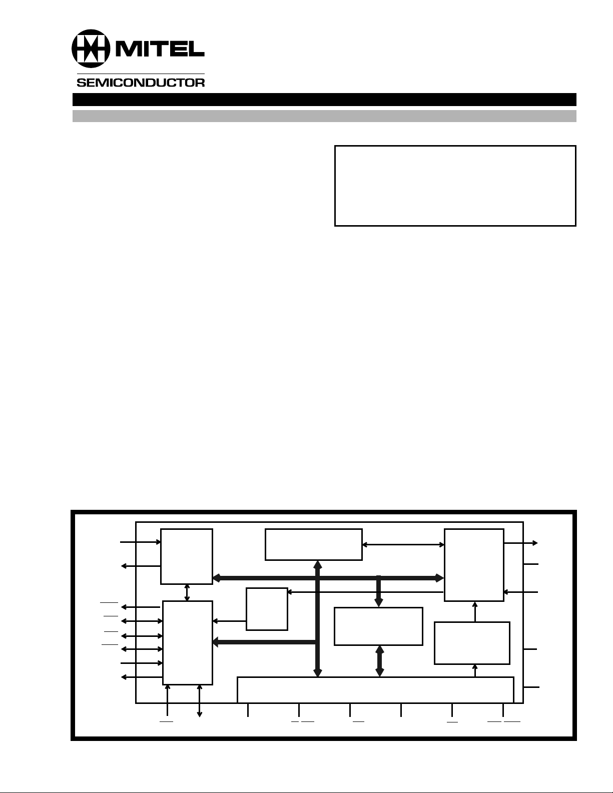
DSTi
DSTo
F0od
C4b
F0b
STAR/Rsto
XTAL1/NT
XTAL2/NC
ST-BUS
Interface
Timing
and
Control
Rsti HALF AD0-7 R/W/WR DS/RD
D-channel Priority
Mechanism
PLL
Microprocessor Interface
Figure 1 - Functional Block Diagram
HDLC
Transceiver
AS/ALE
S-Bus
Interface
Activation
Controller
CS
Link
Link
LTx
VBias
LRx
VDD
VSS
IRQ/NDA
9-71
Page 2
MT8931C
HALF
C4b
F0b
F0od
DSTi
DSTo
XTAL2/NC
XTAL1/NT
W/WR
R/
DS/RD
AS/ALE
CS
IRQ/NDA
VSS
1
2
3
4
5
6
7
8
9
10
11
12
13
14
28 PIN PDIP
28
27
26
25
24
23
22
21
20
19
18
17
16
15
VDD
VBias
LTx
LRx
STAR/
Rsti
AD7
AD6
AD5
AD4
AD3
AD2
AD1
AD0
Rsto
F0od
DSTi
DSTo
NC
NC
NC
XTAL2/NC
XTAL1/NT
NC
W/WR
R/
RD
DS/
NCNCC4b
F0b
HALF
VDD
VBias
NC
AD0
AD1
LTx
AD2
NC
65432 44434241
7
8
9
10
11
12
13
14
15
16
17
NC
AS/ALE
1
231819202122 2425262728
CS
VSS
IRQ/NDA
44 PIN PLCC
NC
39
38
37
36
35
34
33
32
31
30
29
NC
40
LRx
NC
NC
STAR/
Rsti
NC
AD7
AD6
NC
AD5
AD4
AD3
NC
Rsto
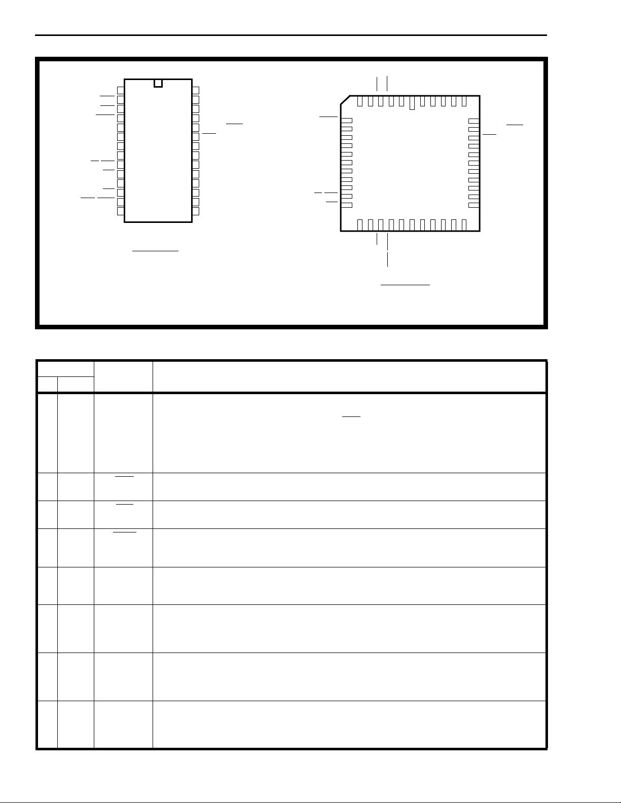
Figure 2 - Pin Connections
Pin Description
Pin #
DIP PLCC
1 2 HALF HALF Input/Output: this is an input in NT mode and an output in TE mode identifying
23 C4b 4.096 MHz Clock: a 4.096 MHz ST-BUS Data Clock input in NT mode.
34 F0b Frame Pulse: an active low frame pulse input indicating the beginning of active ST-
47 F0od Delayed Frame Pulse Output: an active low delayed frame pulse output indicating
5 8 DSTi Data ST-BUS Input: a 2048 kbit/s serial PCM/data ST-BUS input with D, C, B1, and B2
6 9 DSTo Data ST-BUS Output: a 2048 kbit/s serial PCM/data ST-BUS output with D, C, B1 and
7 13 XTAL2/IC Crystal 2/Internal Connection: in TE mode, XTAL1 and XT AL2 are to be connected to
8 14 XTAL1/NT Crystal 1/Network Termination Mode Select Input: for TE mode mode selection, a
Name Description
which half of the S-interface frame is currently being written/read over the ST-BUS
(HALF = 0 sampled on the falling edge of C4b within the frame pulse low window,
identifies the information to be transmitted/received in the first half of the S-Bus frame
while HALF=1 identifies the information to be transmitted/received into the second half
of the S-Bus frame). Tying this pin to VSS or VDD in NT mode will allow the device to free
run. This signal can also be accessed from the ST-BUS C-channel.
In TE mode an output 4.096 MHz clock phase-locked to the line data signal.
BUS channel times in NT mode. Frame pulse output in TE mode.
the end of active ST-BUS channels for this device. Can be used to daisy chain
to other ST-BUS devices to share an ST-BUS stream.
channels assigned to the first four timeslots. These channels contain data to be
transmitted on the line and chip control information.
B2 channels assigned to the first four timeslots, respectively. The remaining timeslots
are placed into high impedance. These channels contain data received from the line
and chip status information.
an external 4.096 MHz parallel resonant crystal for the on-chip oscillator.
If XTAL1 is connected directly to a 4.096 MHz clock, this pin must be left unconnected.
In NT mode, this pin must be left unconnected.
4.096 MHz crystal is to be connected between the XTAL1 and XTAL2 pins, or a 4.096
MHz clock can be connected directly to XTAL1. For NT mode selection, this pin must
be tied to VDD. A pull-up resistor is needed when driven by a TTL device.
9-72
Page 3

MT8931C
Pin Description (continued)
Pin #
DIP PLCC
916R/W/WR Read/Write or Write Input: defines the data bus transfer as a read (R/W=1) or a write
10 17 DS/RD Data Strobe/Read Input: active high input indicates to the SNIC that valid data is on
11 19 AS/ALE Address Strobe/Address Latch Enable Input: in Motorola bus mode the falling edge
12 20 CS Chip Select Input: active low, used to select the SNIC for microprocessor access.
13 21 IRQ
14 22 V
15-2224-26,
30-32,
34-35
23 37 Rsti Reset Input: Schmitt trigger reset input. If ’0’, sets all control registers to the default
24 38 STAR/Rsto Star/Reset (Open Drain Output): 192kbit/s Rx data output fixed relative to the ST-
25 40 LRx Receive Line Signal Input: this is a high impedance input for the pseudoternary line
26 42 LTx Transmit Line Signal Output: this is a current source output designed to drive a
27 43 V
28 44 V
1,5-6,10-
12,15,18,
23,27-
29, 33,
36, 39,
41
Name Description
(R/W=0) in Motorola bus mode. Redefined to WR in Intel bus mode.
the bus during a write operation or that the SNIC must output data during a read
operation in Motorola bus mode. Redefined to RD in Intel bus mode.
is used to strobe the address into the SNIC during microprocessor access. Redefined
to ALE in Intel bus mode.
Interrupt Request (Open Drain Output): an output indicating an unmasked HDLC
interrupt. The interrupt remains active until the microprocessor clears it by reading the
HDLC Interrupt Status Register. This interrupt source is enabled with B2=0 of Master
Control Register.
NDA
New Data Available (Open Drain Output): an active low output signal indicating
availability of new data from the S-Bus. This signal is selected with B2=1 of Master
Control Register. This pin must be tied to VDD with a 10kΩ resistor.
SS
Ground.
AD0-7 Bidirectional Address/Data Bus: electrically and logically compatible to either Intel or
Motorola micro-bus specifications. If DS/RD is low on the rising edge of AS/ALE then
the chip operates to Motorola specs. If DS/RD is high on the rising edge of AS/ALE Intel
mode is selected. Taking Rsti low sets Motorola mode.
conditions, resets activation state machines to the deactivated state, resets HDLC,
clears the HDLC FIFO‘s. Sets the microport to Motorola bus mode.
BUS timebase. A group of NTs, in fixed timing mode, can be wire or’ed together to
create a Star configuration. Active low reset output in TE mode indicating 128
consecutive marks have been received. Can be connected directly to Rsti to allow NT
to reset all TEs on the bus. This pin must be tied to VDD with a 10 kΩ resistor.
signal to be connected to the line through a 2:1 ratio transformer. See Figures 20 and
21. A DC bias level on this input equal to V
must be maintained.
Bias
nominal 50 ohm line through a 2:1 ratio transformer. See Figures 20 and 21.
Bias
Bias Voltage: analog ground for Tx and Rx transformers. This pin must be decoupled
to VDD through a 10µF capacitor with good high frequency characteristics.
DD
Power Supply Input.
NC No Connection.
9-73
Page 4
MT8931C
Functional Description
The MT8931C Subscriber Network Interface Circuit
(SNIC) is a multifunction transceiver providing a
complete interface to the S/T Reference Point as
specified in ETS 300-012, CCITT Recommendation
I.430 and ANSI T1.605. Implementing both
point-to-point and point-to-multipoint voice/data
transmission, the SNIC may be used at either end of
the digital subscriber loop. A programmable digital
interface allows the MT8931C to be configured as a
Network Termination (NT) or as a Terminal
Equipment (TE) device.
The SNIC supports 192 kbit/s (2B+D + overhead) full
duplex data transmission on a 4-wire balanced
transmission line. Transmission capability for both B
and D channels, as well as related timing and
synchronization functions, are provided on chip. The
signalling capability and procedures necessary to
enable customer terminals (TEs) to be activated and
deactivated, form part of the MT8931C’s
functionality. The SNIC handles D-channel resource
allocation and prioritization for access contention
resolution and signalling requirements in passive bus
line configurations. Control and status information
allows implementation of mainten-ance functions
and monitoring of the device and the subscriber loop.
An HDLC transceiver is included on the SNIC for link
access protocol handling via the D-channel.
Depacketized data is passed to and from the
transceiver via the microprocessor port. Two 19 byte
deep FIFOs, one for transmit and one for receive, are
provided to buffer the data. The HDLC block can be
set up to transmit or receive to/from either the
S-interface port or the ST-BUS port. Further, the
transmit destination and receive source can be
independently selected, e.g., transmit to S-interface
while receiving from ST-BUS. The transmit and
receive paths can be separately enabled or disabled.
Both, one and two byte address recognition is
supported by the SNIC. A transparent mode allows
data to be passed directly to the D channel without
being packetized.
A block diagram of the MT8931C is shown in Figure
1. The SNIC has three interface ports: a 4-wire
CCITT compatible S/T interface (subscriber loop
interface), a 2048 kbit/s ST-BUS serial port, and a
general purpose parallel microprocessor port. This
8-bit parallel port is compatible with both Motorola or
Intel microprocessor bus signals and timing.
The three major blocks of the MT8931C, consisting
of the system serial interface (ST-BUS), HDLC
transceiver, and the digital subscriber loop interface
(S-interface) are interconnected by high speed data
busses. Data sent to and received from the
S-interface port (B1, B2 and D channels) can be
accessed from either the parallel microprocessor
port or the serial ST-BUS por t. This is also true for
SNIC control and status information (C-channel).
Depacketized D-channel information to and from the
HDLC section can only be accessed through the
parallel microprocessor port.
S-Bus Interface
The S-Bus is a four wire, full duplex, time division
multiplexed transmission facility which exchanges
information at 192 kbit/s rate including two 64 kbit/s
PCM voice or data channels, a 16 kbit/s signalling
channel and 48 kbit/s for synchronization and
overhead. The relative position of these channels
with respect to the ST-BUS is shown in Figures 4
and 5.
The SNIC makes use of the first four channels on the
ST-BUS to transmit and receive control/status and
data to and from the S-interface port. These are the
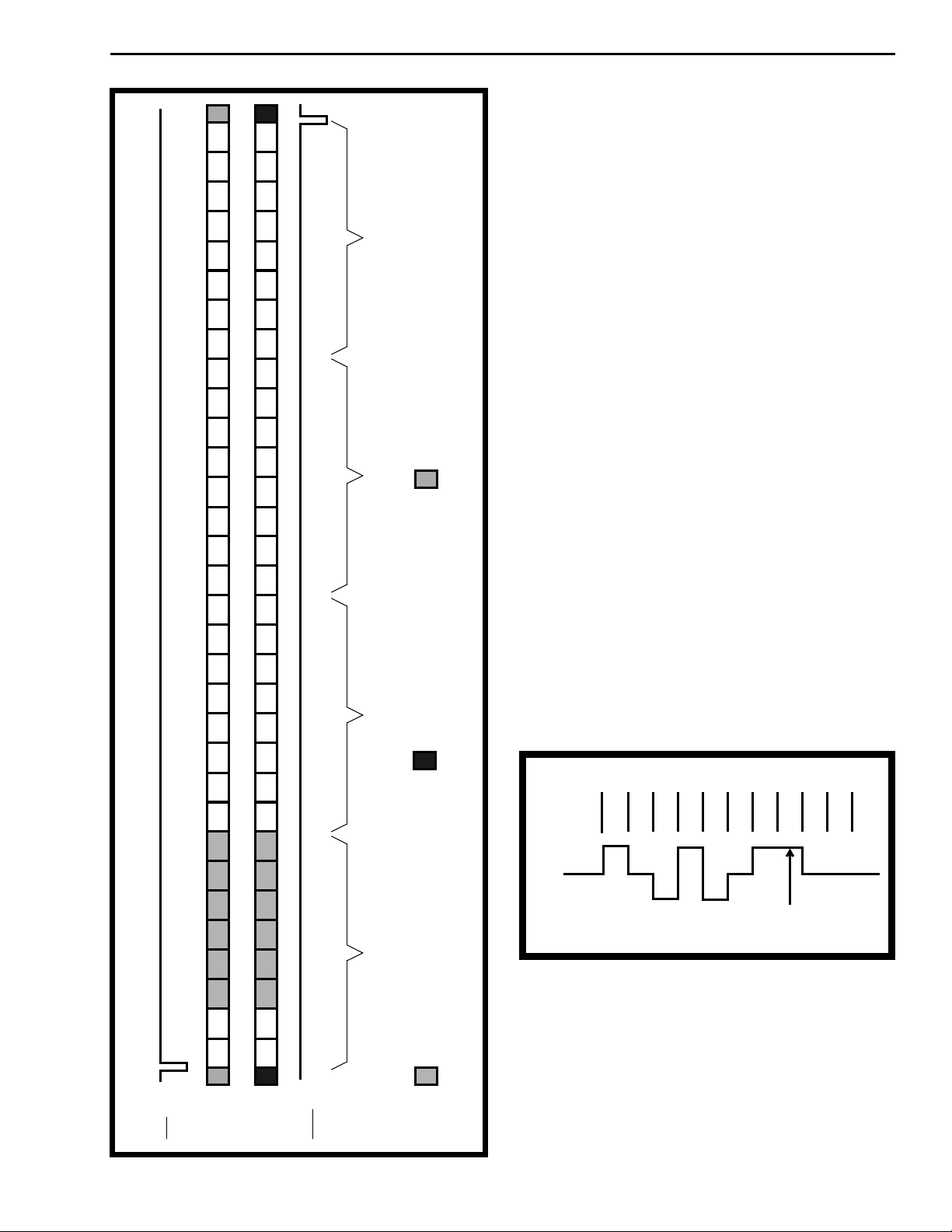
B, D and C-channels (see Figure 4).
9-74
HALF
C4bi
F0bi
F0od
DSTi
DSTo
Cmode
NT
W/WR
R/
RD
DS/
AS/ALE
CS
IRQ/NDA
VSS
NT MODE TE MODE
1
2
3
4
5
6
7
8
9
10
11
12
13
14
28
27
26
25
24
23
22
21
20
19
18
17
16
15
VDD
VBias
LTx
LRx
STAR
Rsti
AD7
AD6
AD5
AD4
AD3
AD2
AD1
AD0
HALF
C4bo
F0bo
F0od
DSTi
DSTo
XTAL2
XTAL1
W/WR
R/
RD
DS/
AS/ALE
CS
IRQ/NDA
VSS
1
2
3
4
5
6
7
8
9
10
11
12
13
14
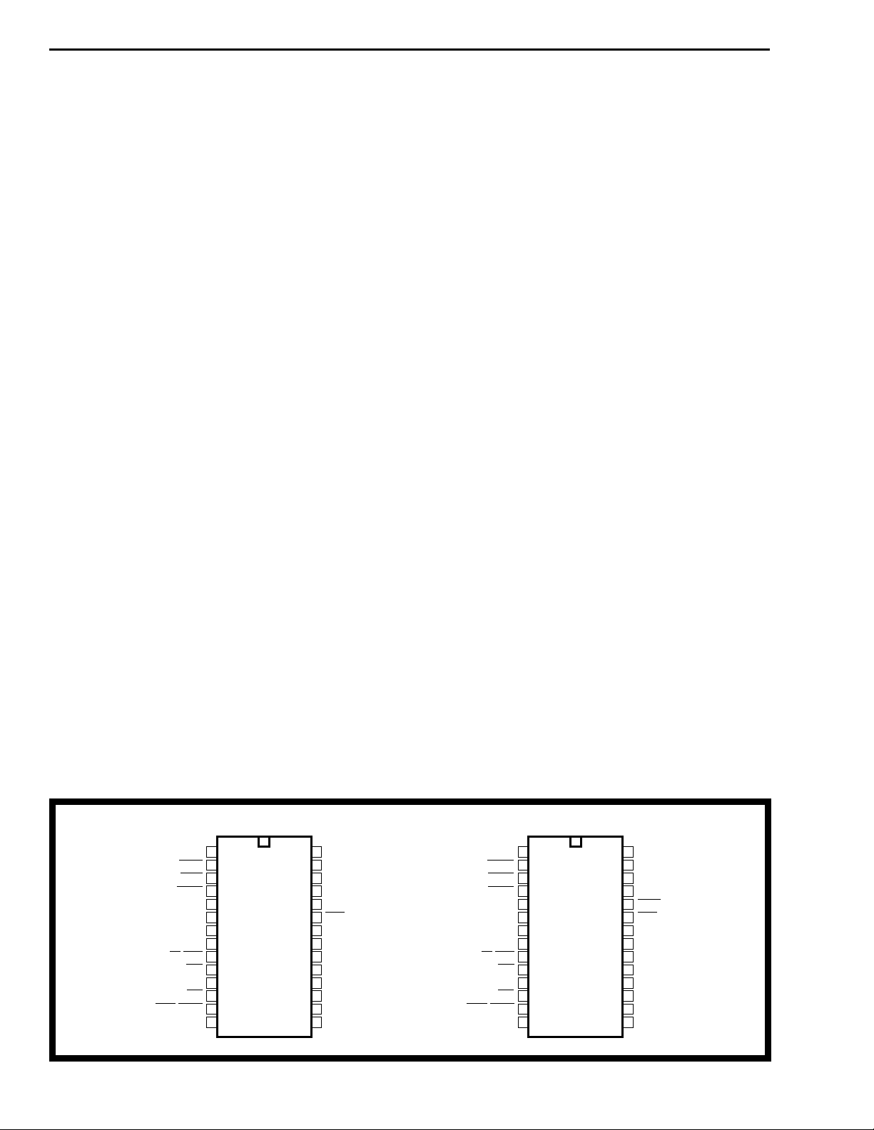
Figure 3 - SNIC Pin Connections
28
27
26
25
24
23
22
21
20
19
18
17
16
15
VDD
VBias
LTx
LRx
Rsto
Rsti
AD7
AD6
AD5
AD4
AD3
AD2
AD1
AD0
Page 5
MT8931C
The B1 and B2 channels each have a bandwidth of
64 kbit/s and are used to carry PCM voice or data
across the network.
The D-channel is primarily intended to carry
signalling information for circuit switching through the
ISDN network. The SNIC provides the capability of
having a 16 kbit/s or full 64 kbit/s D-channel by
allocating the B1-channel timeslot to the D-channel.
Access to the depacketized D-channel is only
granted through the parallel microprocessor port.
The C-channel provides a means for the system to
control and monitor the functionality of the SNIC.
This control/status channel is accessed by the
system through the ST-BUS or microprocessor
port. The C-channel provides access to two
registers which provide complete control over the
state activation machine, the D-channel priority
mechanism as well as the various maintenance
functions. A detailed description of these registers is
discussed in the microprocessor port interface.
B1 B1 B1 B1 B1 B1 B1 B1 B2 B2 B2 B2 B2 B2 B2 B2
C7 C6 C5 C4 C3 C2 C1 C0
D0 D1 D2 D3 D4 D5 D6 D7
B1 B1 B1 B1 B1 B1 B1 B1 B2 B2 B2 B2 B2 B2 B2 B2
C7 C6 C5 C4 C3 C2 C1 C0
D0 D1 D2 D3 D4 D5 D6 D7
Channel 1 (C) Channel 2 (B1) Channel 3 (B2)Channel 0 (D)
Only valid with 64 kbit/s D-channel Output in high impedance state Don’t care
Line Code
The line code used on the S-interface is a Pseudo
ternary code with 100% pulse width as seen in
Figure 5 below. Binary zeros are represented as
marks on the line and successive marks will
alternate in polarity.
BINARY
VALUE
LINE
SIGNAL
0100010011
Violation
Figure 5 - Alternate Zero Inversion Line Code
A mark which does not adhere to the alternating
polarity is known as a bipolar violation.
F0b
DSTi
DSTo
F0od
Figure 4 - ST-BUS Channel Assignment
9-75
Page 6
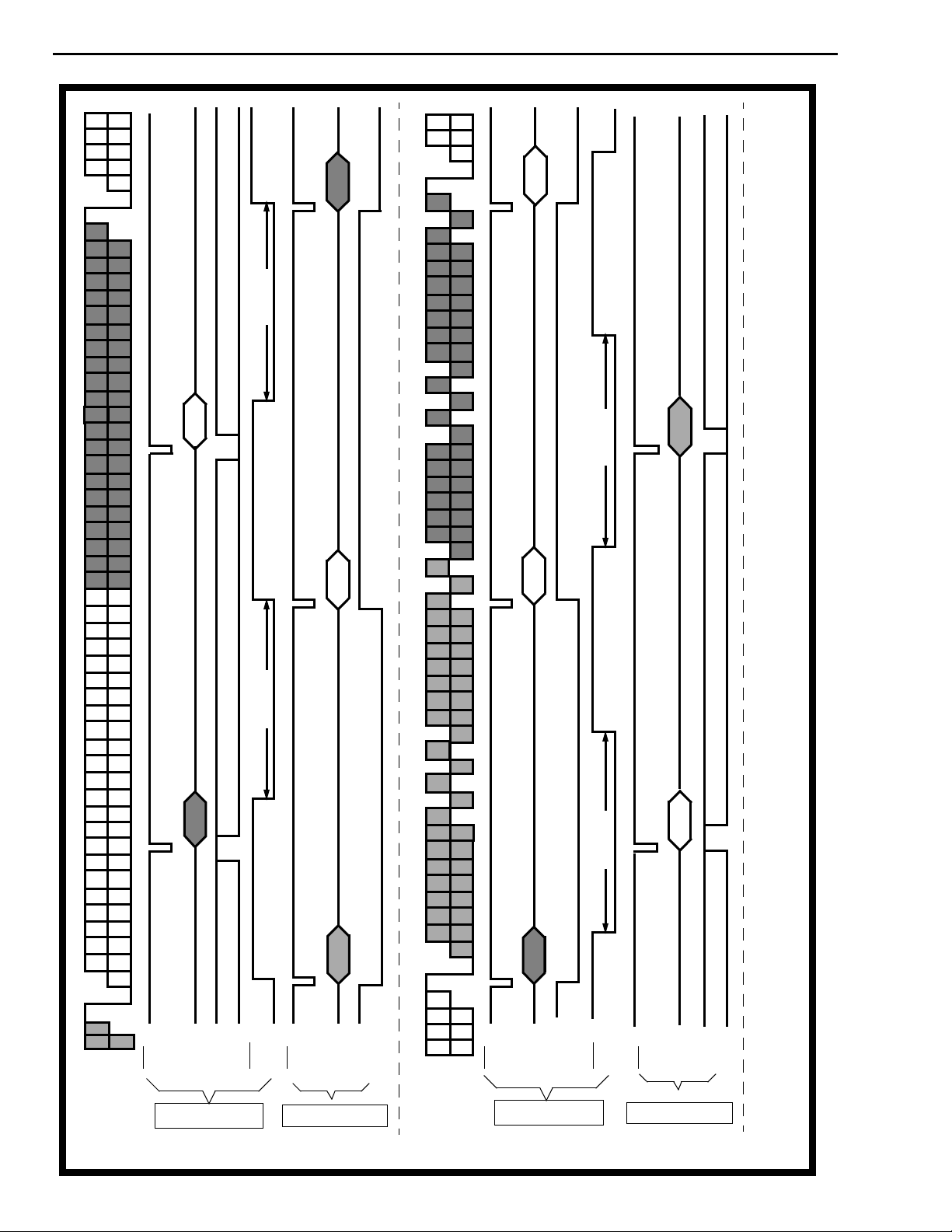
MT8931C
B1 B1B1
62.5 µs
Note: Shaded areas reveal data mapping
B1
B1 B1 B1B1 B1B1 EB1 D0 B2 B2 B2 B2 B2 B2 B2 B2 ES D1 L F L B1 B1FL B1B1 B1B1 B1B1 B1 E D0 A Fa N B2 B2 B2 B2B1 B2 B2 B2 B2 E D1 M B1 B1 B1
B2 L LD1 B1B1 B1B1 B1 B1 B1 L D0 L B2 B2 B2 B2B1 B2 B2 B2 B2 L D1 LB2 L LD1 LFB1B1 B1 B1 B1 B1 B1 L D0 L Fa LB1 B2 B2 B2 B2 B2 B2 B2 FL
62.5 µs
62.5 µs
A = Activation bit
M = Multiframing bit
S = S-channel bit
62.5 µs
Figure 5 - S-Bus Frame Structure and Functional Timing
9-76
NT to TE
F0b
DSTi
NTX
Input
HALF
M
Fa & N (NT to TE) = Auxiliary framing bits
Fa (TE to NT) = Auxiliary framing bit or Q-channel bit
B1 = Bit within B1-channel
B2 = Bit within B2-channel
F0b
DSTi
HALF
NDA
F0b
DSTo
HALF
NDA
F0b
DSTo
HALF
Output
T
TER
C
V
TE to NT
TEX
Output
M
T
NTR
Input
V
C
F = Framing bit
L = DC balancing bit
D = Bit within D-channel
E = D-echo channel bit
Page 7
MT8931C
Framing
The valid frame structure transmitted by the NT and
TE contains the following (refer Fig. 6):
NT to TE:
- Framing bit (F)
- B1 and B2 channels (B1,B2)
- DC balancing bits (L)
- D-channel bits (D0, D1)
- Auxiliary framing and N bit (Fa, N), N=Fa
- Activation bit (A)
- D-echo channel bits (E)
- Multiframing bit (M)
- S-channel bit
TE to NT:
- Framing bit (F)
- B1 and B2 channels (B1, B2)
- DC balancing bits (L)
- D-channel bits (D0, D1)
- Auxiliary framing bit (Fa) or Q-channel bit
The framing mechanism on the S-interface makes
use of line code violations to identify frame
boundaries. The F-bit violates the alternating line
code sequence to allow for quick identification of the
frame boundaries. To secure the frame alignment,
the next mark following the frame balancing bit
(L) will also produce a line code violation. If the
data following the balancing bit is all binary ones,
the zero in the auxiliary framing bit (Fa) or N-bit (for
the direction NT to TE) will provide successive
violations to ensure that the 14 bit criterion (13 bit
criterion in the direction TE to NT) specified in
Recommendations I.430 and T1.605 is satisfied. If
the B1-channel is not all binary ones, the first zero
following the L-bit will violate the line code sequence,
thus allowing subsequent marks to alternate without
bipolar violations.
The Fa and N bits can also be used to identify a
multiframe structure (when this is done, the 14 bit
criterion may not be met). This multiframe structure
will make provisions for a low speed signalling
channel to be used in the TE to NT direction
(Q-channel). It will consist of a five frame multiframe
which can be identified by the binary inversion of the
Fa and N-bit on the first frame and consequently on
every fifth frame of the multiframe . Upon detection of
the multiframe signal, the TE will replace the next Fabit to be transmitted with the Q-bit.
The A-bit is used by the NT during line activation
procedures (refer to state activation diagrams). The
state of the A-bit will advise the TE if the NT has
achieved synchronization.
The E-bit is the D-echo channel. The NT will reflect
the binary value of the received D-channel into the
E-bits. This is used to establish the access
contention resolution in a point-to-multipoint
configuration. This is described in more detail in the
section of the D-channel priority mechanism.
The M-bit is a second level of multiframing which is
used for structuring the Q-bits. The frame with Mbit=1 identifies frame #1 in the twenty frame
multiframe. The Q-channel is then received as
shown in Table 1. All synchronization with the
multiframes must be performed externally.
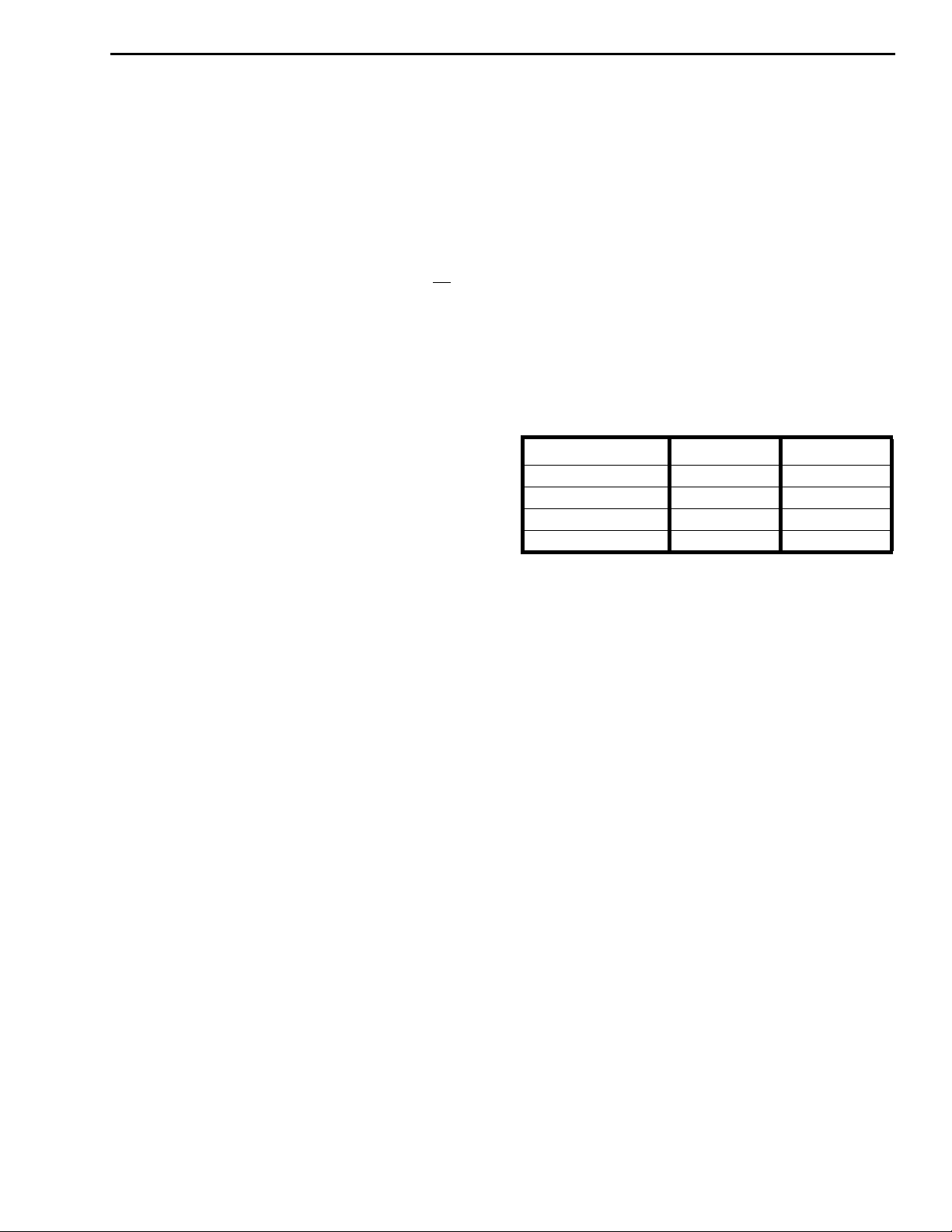
FRAME # Q-BIT M-BIT
1Q11
6Q20
11 Q3 0
16 Q4 0
Table 1. Q-channel Allocation
Bit Order
When using the B-channels for PCM voice, the first
bit to be transmitted on the S-Bus should be the sign
bit. This complies with the existing telecom
standards which transmit PCM voice as most
significant bit first. However, if the B-channels are to
carry data, the bit ordering must be reversed to
comply with the existing datacom standards (i.e.,
least significant bit first).
These contradicting standards place a restriction on
all information input and output through the serial
and parallel ports. Information transferred through
the serial ports, will maintain the integrity of the bit
order. Data sent to either serial port from the parallel
port, will transmit the least significant bit first.
Therefore, a PCM byte input through the
microprocessor port must be reordered to have the
sign bit as the least significant bit.
When the microprocessor reads D, B1 or B2 channel
data of either ST-BUS or S-bus serial por t, the least
significant bit read is the first bit received on that
particular channel of either serial port.
The DC balancing bits (L) are used to remove any
DC content from the line. The balancing bit will be a
mark if the number of preceding marks up to the
previous balancing bit is odd. If the number of marks
is even, the L-bit will be a space.
The D-channel received on the serial ST-BUS por ts
must be ordered with the least significant bit first as
shown in Figure 4. This also applies to the
D-channel directed to the ST-BUS from the
microprocessor port.
9-77
Page 8
MT8931C
The C-channel bit mapping from the parallel port to
the ST-BUS is organized such that the most
significant bit is transmitted or received first.
State Activation
The state activation controller activates or
deactivates the SNIC in response to line activity or
external command. The controller is completely
hardware driven and need not be initialized by the
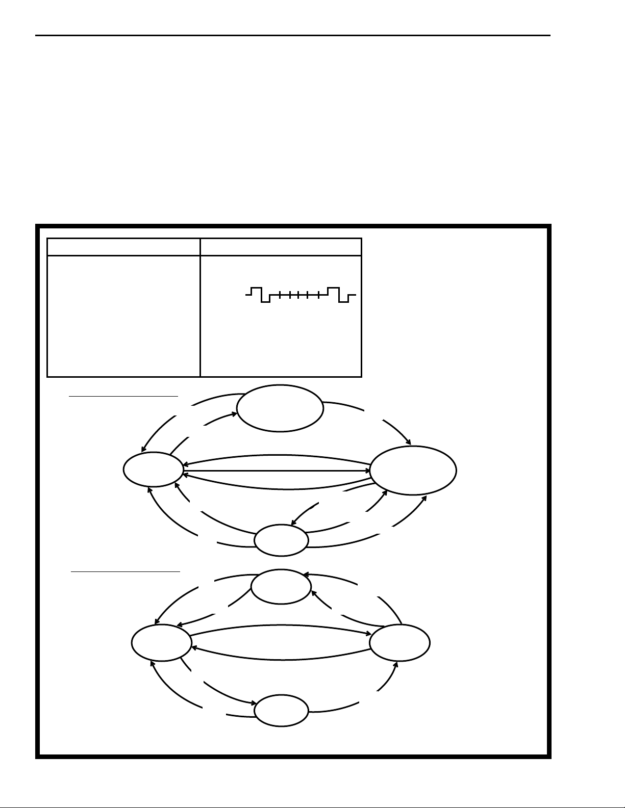
microprocessor. The state diagram for initialization
is shown in Figure 7.
Signals from NT to TE Signals from TE to NT
Info0
Info2
Info4
No Signal
Valid frame structure with
all B, D, D-echo and A bits
set to ‘0’
Valid frame with data in B,
D, D-echo channels. Bit A is
set to 1.
TE State Activation Diagram
DR = 1
Info0 No Signal
Info1 Continuous Signal of +‘0’, -‘0’
Info3 Valid frame with data in B & D
AR = 1
and six ‘1’s
Bits
Activation Request
send Info1 if BA = 0
send Info0 if BA = 1
The protocol used by the state activation controller is
defined as follows:
1) In the deactivated state, neither the NT nor TE
assert a signal on the line (Info0).
2) If the TE wants to initiate activation, it must begin
transmitting a continuous signal consisting of a
positive zero, a negative zero followed by six
ones (Info1).
3) Once the NT has detected Info1, it begins to
transmit Info2 which consists of an S-Bus frame
Where: BA
(1)
Note 1: signal is not timebase locked to NT.
Note 2: Sync/BA bit of the Status Register
Sync = 1
(2)
= Bus Activity
DR = Deactivation Request
AR = Activation Request
(2)
Sync
= Frame Sync Signal
A = Activation bit
Time out = 32 ms Timer Signal
is configured as Sync bit when
AR = 1 and DR = 0, or as BA bit
when AR = 0 or DR = 1. A change in
the state of the AR and/or DR bits
will cause a change in the function
of the Sync/BA bit in the following
ST-BUS frame.
Deactivated
send Info0
NT State Activation Diagram
Pending
Activation
send Info2
DR = 1
BA = 0
BA = 1
AR = 1
Sync = 1
Sync = 0
BA = 0
Sync = 1
DR = 1
Activated
send Info3
Deactivated
send Info0
DR = 1
AR = 1
Activated
send Info4
Synchronized
send Info3 if Sync = 1
send Info0 if Sync = 0
A = 1 &
Sync = 1
Sync = 0
A = 0
Time out
BA =0
Pending
Deactivation
Send Info0
DR = 1
9-78
Figure 7 - Link Activation Protocol, State Diagram
Page 9
MT8931C
with zeros in the B and D-channel and the
activation bit (A-bit) set to zero.
4) As soon as the TE synchronizes to Info2, it
responds with a valid S-Bus frame with data in
the B1, B2 and D-channel (Info3).
5) The NT will then transmit a valid frame with data
in the B1, B2 and D-channel. It will also set the
activation bit (A) to binary one once
synchronization to Info3 is achieved.
If the NT wishes to initiate the activation, steps 2 and
3 are ignored and the NT starts sending Info2. To
initiate a deactivation, either end begins to send
Info0 (Idle line).
D-channel Priority Mechanism
The SNIC contains a hardware priority mechanism
for D-channel contention resolution. All TEs
connected in a point-to-multipoint configuration are
allocated the D-channel using a systematic
approach. Allocation of the D-channel is
accomplished by monitoring the D-echo channel
(E-bit) and incrementing the D-channel priority
counter with every consecutive one echoed back in
the E bit. Any zero found on the D-echo channel will
reset the priority counter.
There are two classes of priority within the SNIC,
one user accessible and the other being strictly
internal. The user accessible priority selects the
class of operation and has precedence over the
internal priority. The latter (internal priority), will
select the level of priority within each class (i.e., the
internal priority is a subsection of the user accessible
priority). User accessible priority selects the
terminal count as 8/9 or 10/11 consecutive ones on
the E-bit (8 being high priority while 10 being low
priority). The internal priority selects the terminal
between 8 or 9 for high class and 10 or 11 for low
class. The first terminal equipment to attain the E-bit
priority count will immediately take control of the
D-channel by sending the opening flag. If more than
one terminal has the same priority, all but one of
them will eventually detect a collision. The TEs that
detect a collision will immediately stop trans-mitting
on the D-channel, generate an interrupt through the
Dcoll bit, reset the DCack bit on the next frame
pulse, and restart the counting process. The
remainder of the packet in the Tx FIFO is ignored.
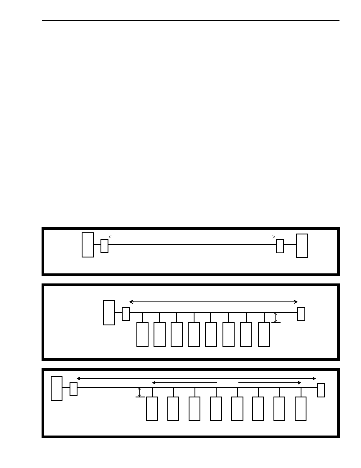
NT
NT is operating in adaptive timing
TR is the line termination resistor = 100 Ω
NT is operating in fixed timing
TR is the line termination resistor = 100 Ω
T
R
NT
T
R
Figure 9 - Short Passive Bus Configuration, up to 8 TEs can be supported
NT
T
R
0 - 10 m
0 - 1 Km
Figure 8 - Point-to-Point Configuration
100 m for 75 Ω impedance cable and 200 m for 150 Ω impedance cable
TE
TE TE TE TE TE TE TE
100 - 200 m
0-500 m
0-50 m
T
R
0 - 10 m
TE
T
R
T
R
NT is operating in adaptive timing
TR is the line termination resistor = 100 Ω
Figure 10 - Extended Passive Bus Configuration, up to 8 TEs can be supported
TE TE TE TE TE TE TE
TE
9-79
Page 10
MT8931C
After successfully completing a transmission, the
internal priority level is reduced from high to low.
The internal priority will only be increased once the
terminal count for the respective level of priority has
been achieved. (e.g., if TE has high priority
internally and externally, it must count 8 consecutive
ones in the D-echo channel. Once this is achieved
and successful transmission has been completed,
the internal priority is reduced to a lower level (i.e.,
count = 9). This terminal will not return to the high
internal priority until 9 consecutive ones have been
monitored on the D-echo channel).
Line Wiring Configuration
The MT8931C can interface to any of the three
wiring configurations which are specified by the
CCITT Recommendation I.430 and ANSI T1.605
(refer to Figures 8 to 10). These consist of a
point-to-point or one of the two point-to- multipoint
configurations (i.e., short passive bus or the
extended passive bus). The selection of line
configurations is performed using the timing bit (B4
of NT Mode Control Register).
For the short passive bus, TE devices are connected
at random points along the cable. However, for the
extended passive bus all connection points are
grouped at the far end of the cable from the NT.
For an NT SNIC in fixed timing mode, the VCO and
Rx filters/peak detectors are disabled and the
threshold voltage is fixed. Ho w ever, for a TE SNIC or
an NT SNIC (in adaptive timing mode), the VCO and
Rx filters/peak detectors are enabled. In this
manner, the device can compensate for variable
round trip delays and line attenuation using a
threshold voltage set to a fixed percentage of the
pulse peak amplitude.
Another operation can be implemented using the
SNIC in the star configuration as shown in Figure 14.
This mode allows multiple NTs, with physically
independent S-Busses, to share a common input
source and transfer inf ormation down the S-Bus to all
TEs . All NT devices connected into the star will
receive the information transmitted by all TEs on all
branches of the star, exactly as if they were on the
same physical S-Bus. All NTs in the star
configuration must be operating in fixed timing mode.
Refer to the description of the star configuration in
the ST-BUS section.
The SNIC has one last mode of operation called the
NT slave mode. This has the effect of operating the
SNIC in network termination mode (XTAL1/NT pin =
1) but having the frame structure and registers
description defined by the TE mode. This can be
used where multiple subscriber loops must carry a
fixed phase relation between each line. A typical
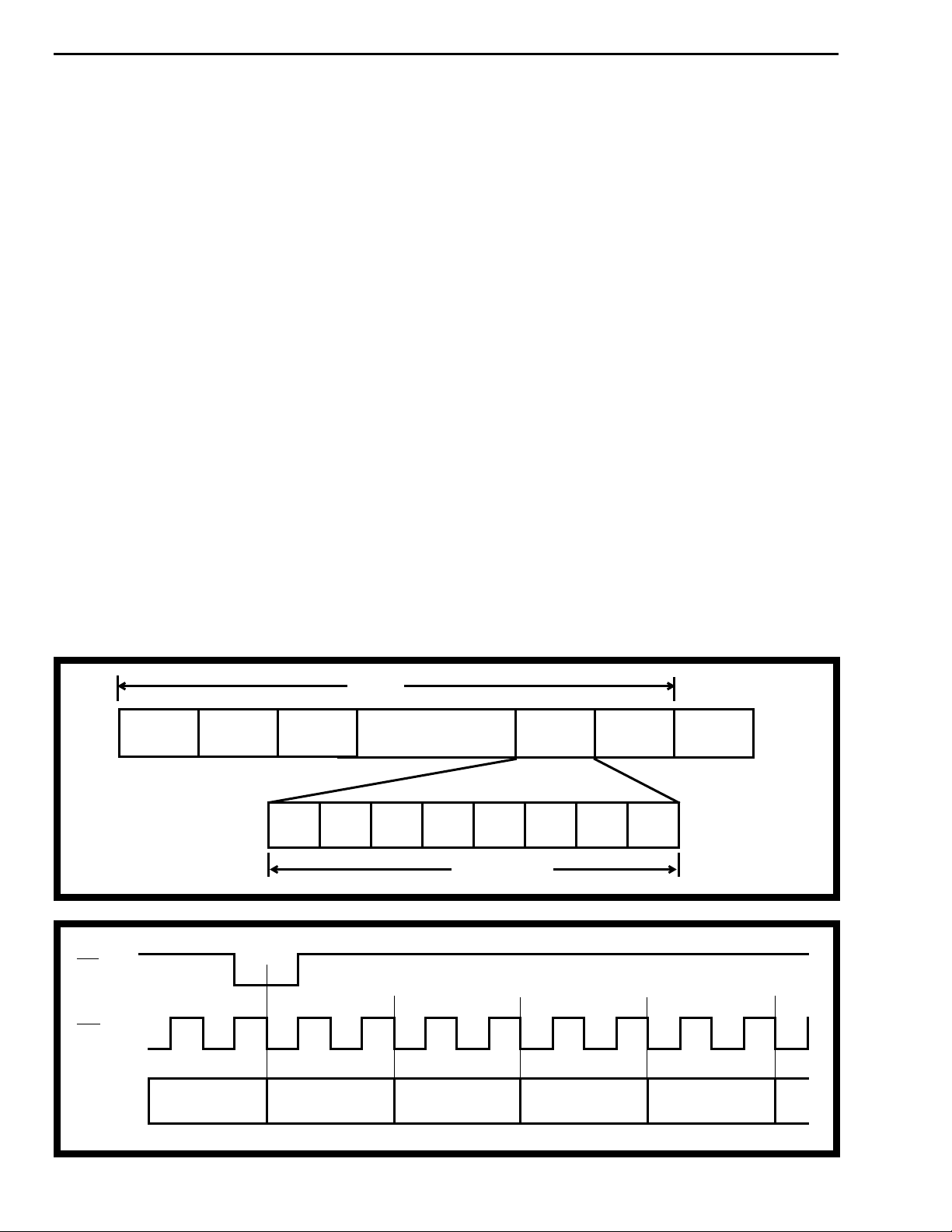
F0b
C4b
ST-BUS
BIT CELLS
Channel0Channel
1
Channel 31
Bit 0
125 µs
Channel
2
Bit 7 Bit 6 Bit 5 Bit 4 Bit 3 Bit 2 Bit 1 Bit 0
•••
(8/2048) ms
Channel30Channel31Channel
Figure 11 - ST-BUS Stream Format
Channel 0
Bit 7
Channel 0
Bit 6
Channel 0
Bit 5
0
Channel 0
Bit 4
9-80
Figure 12 - Clock & Frame Alignment for ST-BUS Streams
Page 11
MT8931C
situation is when the system is trying to synchronize
two nodes of a synchronous network. This allows
multiple TEs to share a common ST-BUS timebase.
The synchronization of the loops is established by
using the clock signals produced by a local TE as an
input timing source to the NT slave.
Adaptive Timing Operation
On power-up or after a reset, the SNIC in NT mode is
set to operate in fixed timing. To switch to adaptive
timing, the user should:
1) set the DR bit to 1
2) set the Timing bit to 1 in the C-channel
Control Register
3) wait for 100 ms period
4) proceed in using the AR and DR bits as
desired
Switching from adaptive timing mode is completed
by resetting the Timing bit.
ST-BUS Interface
The ST-BUS is a synchronous time division
multiplexed serial bussing scheme with data streams
operating at 2048 kbit/s configured as 32, 64 kbit/s
channels (refer to Fig. 11). Synchroni-zation of the
data transfer is provided from a frame pulse which
identifies the frame boundaries and repeats at an 8
kHz rate. Figure 4 shows how the frame pulse
(F0b) defines the ST-BUS frame boundaries. All
data is clocked into the device on the rising edge of
the 4096 kHz clock (C4b) three quarters of the way
into the bit cell, while data is clocked out on the
falling edge of the 4096 kHz clock at the start of the
bit cell.
All timing signals (i.e. F0b & C4b) are identified as
bidirectional (denoted by the terminating b). The
I/O configuration of these pins is controlled by the
mode of operation (NT or TE). In the NT mode, all
synchronized signals are supplied from an external
source and the SNIC uses this timing while
transferring information to and from the S or
ST-BUS. In the TE mode, an on-board analog
phase-locked loop extracts timing from the received
data on the S-Bus and generates the system
4096 kHz (C4b) and frame pulse (F0b). The
analog phase-locked loop also maintains proper
phase relation between the timing signals as well as
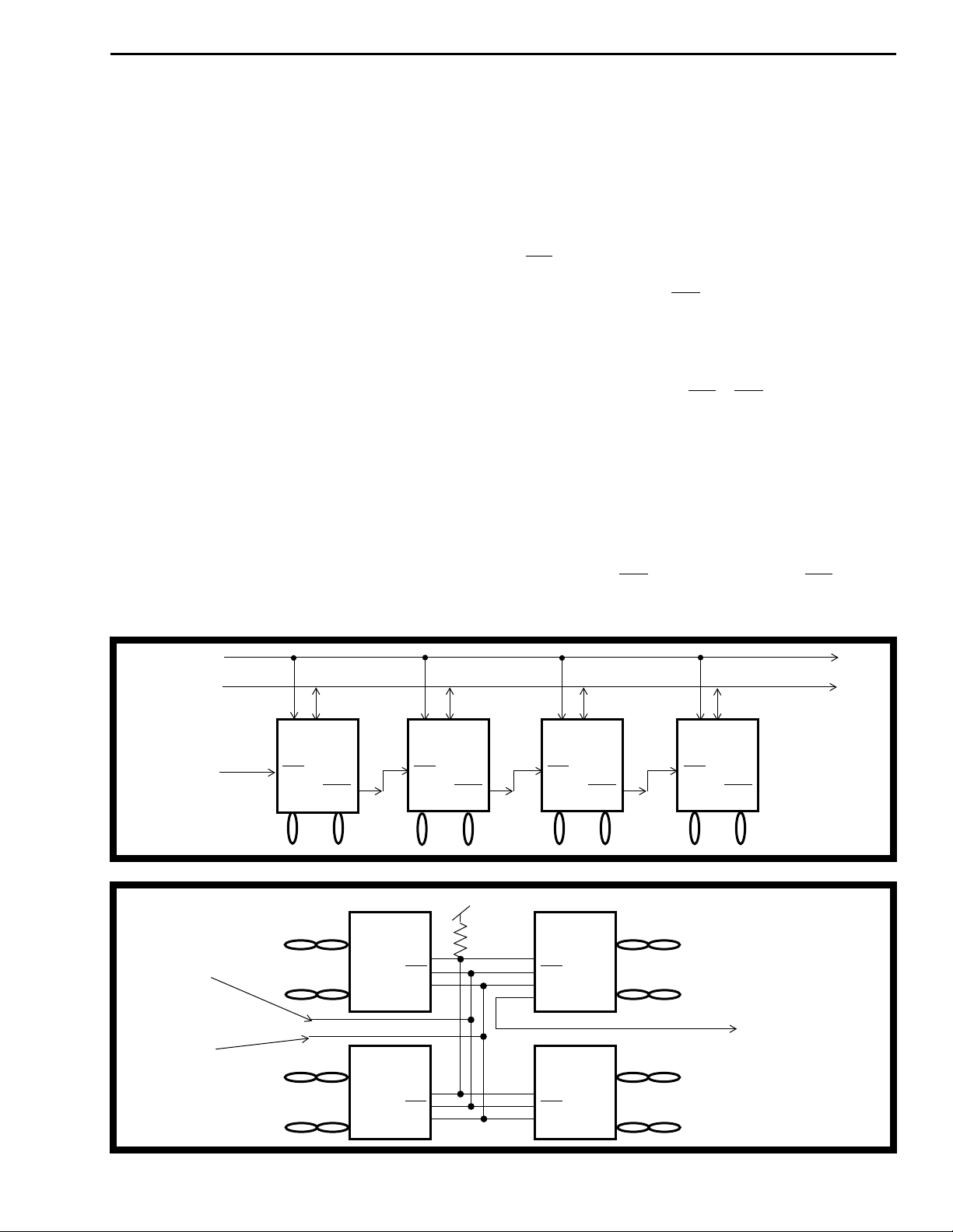
ST-BUS Clock
ST-BUS
Stream
System
Frame Pulse
System
Frame Pulse
Input
ST-BUS Stream
Active on
Channel 0 - 3
MT8931C
NT
F0b
F0od
to TE to TE to TE to TE
MT8931C
F0b
Active on
Channels 4 - 7
NT
F0od
Active on
Channels 8 - 11
MT8931C
NT
F0b
F0od
Figure 13 - Daisy Chaining the SNIC
V
DD
to TE
to TE
MT8931C
NT
STAR
F0b
DSTi
MT8931C
NT
STAR
F0b
DSTi
MT8931C
NT
STAR
F0b
DSTi
DSTo
MT8931C
NT
STAR
F0b
DSTi
to TE
to TE
Active on
Channels 12 - 15
MT8931C
NT
F0b
F0od
Output
ST-BUS Stream
Figure 14 - NT in Star Configuration
9-81
Page 12

MT8931C
filtering out jitter which may be present on the
received line port.
The SNIC uses the first four channels on the
ST-BUS (as shown in Figure 4). To simplify the
distribution of the serial stream, the SNIC
provides a delayed frame pulse (F0od) to eliminate
the need for a channel assignment circuit. This
signal is used to drive subsequent devices in the
daisy chain (refer Figure 13). In this type of
arrangement, only the first SNIC in the chain will
receive the system frame pulse (F0b) with the
following devices receiving its predecessor’s delayed
output frame pulse (F0od).
The SNIC makes efficient use of its TDM bus
through the Star configuration. It does so by sharing
four common ST-BUS channels to multiple NT
devices. Up to eight SNICs in NT mode with
physically independent S-Busses can be connected
in parallel to realize a star configuration (as shown in
Figure 14). All devices connected into the star will
carry the same input, thus information is sent to all
TEs simultaneously. The 2B+D data received from
every TE is transmitted to all NTs through the STAR
pin. Consequently, all the DSTo streams will carry
identical 2B+D data reflecting what is being
transmitted by the various TEs.
The flow of data in the direction of S-Bus to ST-BUS
is transparent to the SNIC, regardless of the state
machine status. On the other hand, the flow of data
in the direction of ST-BUS to S-Bus becomes
transparent only after the state machine is in the
active state (IS0, IS1=1,1), in case of an NT, or in the
synchronization state (IS0, IS1=1), in case of a TE.
Microprocessor/Control Interface
The microprocessor port is compatible with either
Motorola or Intel multiplexed bus signals and timing.
The MOTEL circuit (MOtorola and InTEL
Compatible bus) uses the level of the DS/RD pin
at the rising edge of AS/ALE to select the
appropriate bus timing. If DS/RD is low at the
rising edge of AS/ALE (refer to Figure 26) then
Motorola bus timing is selected. Conversely, if DS/
RD is high at the rising edge of AS/ALE (refer to
Figures 24 & 25), then Intel bus timing is selected.
This has the effect of redefining the microprocessor
port transparently to the user.
The user has the option of writing to the C-channel
Control or Diagnostic Register through the parallel
port interface or through the C-channel on DSTi. Bit
0 of the Master Control Register provides this option.
Address Lines
A4 A3 A2 A1 A0
0 0 0 0 0 Master Control Register verify
A 0 0 0 0 1 ST-BUS Control Register verify
S 0 0 0 1 0 HDLC Control Register 1 verify
Y 0 0 0 1 1 HDLC Control Register 2 HDLC Status Register
N 0 0 1 0 0 HDLC Interrupt Mask Register HDLC Interrupt Status Register
C 0 0 1 0 1 HDLC Tx FIFO HDLC Rx FIFO
0 0 1 1 0 HDLC Address Byte #1 Register verify
0 0 1 1 1 HDLC Address Byte #2 Register verify
0 1 0 0 0 C-channel Control Register
0 1 0 0 1 C-channel Status Register
1 0 0 0 0 Control Register 1 Not Available
1 0 0 1 0 Not Available Master Status Register
0 1 0 0 0 DSTi C-channel
0 1 0 0 1 DSTo C-channel
S 0 1 0 1 0 S-Bus Tx D-channel DSTi D-channel
Y 0 1 0 1 1 DSTo D-channel S-Bus Rx D-channel
N 0 1 1 0 0 S-Bus Tx B1-channel DSTi B1-channel
C 0 1 1 0 1 DSTo B1-channel S-Bus Rx B1-channel
0 1 1 1 0 S-Bus Tx B2-channel DSTi B2-channel
0 1 1 1 1 DSTo B2-channel S-Bus Rx B2-channel
Table 2. SNIC Address Map
Write Read
9-82
Page 13

MT8931C
The parallel port on the SNIC allows complete
control of the HDLC transceiver and access to all
data, control and status registers. Reading these
registers allows the microprocessor to monitor
incoming data on the S or ST-BUS without
interrupting the normal data flow.
Some registers are classified as asynchronous and
others as synchronous. Synchronous registers are
single-buffered and require synchronous access.
Not all the synchronous registers have the same
access times, but all can be accessed
synchronously in the time during which the NDA
signal is low (refer to Fig. 5). Therefore, it is
recommended that the user make use of the NDA
signal to access these registers. Since the
synchronous registers use common circuitry, it is
essential that the register be read before being
written. This sequence is important as a write cycle
will overwrite the last data received. These parallel
accesses must be refreshed every frame.
Asynchronous registers, on the other hand, can be
accessed at any time.
The data in TE or NT Mode Status Register,
depending upon the mode selected, is always sent
out on the C-channel of DSTo. However, in
microprocessor control mode the user can overwrite
this data by writing to the DSTo C-channel Register.
This access can be done anytime outside the frame
pulse interval of the ST-BUS frame. Data written in
the current ST-BUS frame will only appear in the Cchannel of the following frame.
HDLC Transceiver
The HDLC Transceiver handles the bit oriented
protocol structure and formats the D-channel as per
level 2 of the X.25 packet switching protocol defined
by CCITT. It transmits and receives the packetized
data (information or control) serially in a format
shown in Figure 15, while providing data
transparency by zero insertion and deletion. It
generates and detects the flags, various link channel
states and the abort sequence. Further, it provides a
cyclic redundancy check on the data packets using
the CCITT defined polynomial. In addition, it can
recognize a single byte, dual byte or an all call
address in the received frame. There is also a
provision to disable the protocol functions and
provide transparent access to either serial port
through the microprocessor port. Other features
provided by the HDLC include, independent port
selection for transmit and received data (e.g.
transmit on S-Bus and receive from ST-BUS),
selectable 16 or 64 kbit/s D-channel as well as an
HDLC loopback from the transmit to the receive port.
These features are enabled through the HDLC
control registers (see Tables 6 and 7).
HDLC Frame Format
All frames start with an opening flag and end with a
closing flag as shown in Figure 15. Between these
two flags, a frame contains the data and the frame
check sequence (FCS).
The least significant bit (B0) of the C-channel
Register, selects between the control register or the
diagnostic register. Setting the B0 of the C-channel
Register to ’0’ allow access to the control register.
Setting the LSB of the C-channel Register to ’1’ allow
access to the diagnostic register. The interpretation
of each register is defined in Tables 13 and 14 for NT
mode or Tables 16 and 17 for the TE mode.
It is important to note that in TE mode, the C-channel
Diagnostic Register should be cleared while the
device is not in the active state (IS0, IS1 ≠ 1,1). This
is accomplished by setting the ClrDia bit of the Cchannel Control Register to 1 until the device is
activated. In serial control mode, the C-channel on
the ST-BUS is loaded into the C-channel Control
Register in every ST-BUS frame; the user should
make sure that a 1 is written to the ClrDia bit in every
frame. However, in parallel control mode the user
needs to set the ClrDia bit only once to keep the
Diagnostic Register cleared. Once full activation is
achieved the Diagnostic Register can be written to in
order to enable the various test functions.
FLAG DATA FIELD FCS FLAG
One
Byte
i) Flag
The flag is a unique pattern of 8 bits (01111110)
defining the frame boundary. The transmit section
generates the flags and appends them automatically
to the frame to be transmitted. The receive section
searches the incoming packets for flags on a
bit-by-bit basis and establishes frame
synchronization. The flags are used only to identify
and synchronize the received frame and are not
transferred to the FIFO.
n Bytes
(n ≥ 2)
Figure 15 - Frame Format
Two
Bytes
One
Byte
9-83
Page 14

MT8931C
ii) Data
The data field refers to the Address, Control and
Information fields defined in the CCITT
recommendations. A valid frame should have a data
field of at least 16 bits. The first and second byte in
the data field is the address of the frame.
iii) Frame Check Sequence (FCS)
The 16 bits following the data field are the frame
check sequence bits. The generator polynomial is:
G(x)=x16+x12+x5+1
The transmitter calculates the FCS on all bits of the
data field and transmits the complement of the FCS
with most significant bit first. The receiver performs
a similar computation on all bits of the received data
but also includes the FCS field. The generating
polynomial will assure that if the integrity of of the
transmitted data was maintained, the remainder will
have a consistent pattern and this can be used to
identify, with high probability, any bit errors occurred
during transmission. The error status of the received
packet is indicated by B7 and B6 bits in the HDLC
Status Register.
Interframe Time Fill
When the HDLC Tranceiver is not sending packets,
the transmitter can be in one of two states mentioned
below depending on the status of the IFTF bit in the
HDLC Control Register 1.
i) Idle State
The Idle state is defined as 15 or more contiguous
ONEs. When the HDLC Protocoller is observing this
condition on the receiving channel, the Idle bit in the
HDLC Status Register is set HIGH. On the transmit
side, the Protocoller ends the transmission of all
ones (idle state) when data is loaded into the
transmit FIFO.
CCITT I.430 Specification requires every TE that
does not have layer 2 frames to transmit, to send
binary ONEs on the D-channel. In this manner, other
TEs on the line will have the opportunity to access
the D-channel using the priority mechanism circuitry.
ii) Flag Fill State
iv) Zero Insertion and Deletion
The transmitter, while sending either data from the
FIFO or the 16 bits FCS, checks the transmission on
a bit-by-bit basis and inserts a ZERO after every
sequence of five contiguous ONEs (including the last
five bits of FCS) to ensure that the flag sequence is
not imitated. Similarly the receiver examines the
incoming frame content and discards any ZERO
directly following the five contiguous ONEs.
v) Abort
The transmitter aborts a frame by sending a zero
followed by seven consecutive ONEs. The FA bit in
the HDLC Control Register 2 along with a write to the
HDLC Transmit FIFO enables the transmission of an
abort sequence instead of the byte written to the
register (to have a valid abor t there must be at least
two bytes in the packet). On the receive side, a
frame abort is defined as seven or more contiguous
ONEs occurring after the start flag and before the
end flag of a packet. An interrupt can be generated
on reception of the abort sequence using FA bit in
the HDLC Interrupt Mask/Vector Registers (refer to
Tables 9 and 10).
The HDLC Protocoller transmits continuous flags
(7E
) in Interframe Time Fill state and ends this
Hex
state when data is loaded into the transmit FIFO.
The reception of the interframe time fill will have the
effect of setting the idle bit in the HDLC Status
Register is set to ’0’.
HDLC Transmitter
On power up, the HDLC transmitter is disabled and
in the idle state. The transmitter is enabled by
setting the TxEN bit in the HDLC Control Register 1.
To start a packet, the data is written into the 19 byte
Transmit FIFO starting with the address field. All the
data must be written to the FIFO in a bytewide
manner. When the data is detected in the transmit
FIFO, the HDLC protocoller will proceed in one of the
following ways:
1) If the transmitter is in idle state, the present byte
of ones is completely transmitted before sending
the opening flag. The data in the transmit FIFO
is then transmitted. A TE transmitting on the Dchannel will use the contention circuitry
described previously in
Mechanism
to access this channel.
D-channel Priority
9-84
2) If the transmitter is in the flag fill state, the
flag presently being transmitted is used as the
opening flag for the packet stored in the transmit
FIFO.
Page 15

MT8931C
3) If the HDLC transmitter is in transparent
data mode, the protocol functions are disabled
and the data in the transmit FIFO is transmitted
without a framing structure.
To indicate that the particular byte is the last byte of
the packet, the EOP bit in the HDLC Control Register
2 must be set before the last byte is written into the
transmit FIFO. The EOP bit is cleared automatically
when the data byte is written to the FIFO. After the
transmission of the last byte in the packet, the frame
check sequence (16 bits) is sent followed by a
closing flag. If there is any more data in the transmit
FIFO, it is immediately sent after the closing flag.
That is, the closing flag of a packet is also used as
the opening flag the the next packet.
However, CCITT I.430 and ANSI T1.605
Recommendations state that after the successful
transmission of a packet, a TE must lower its priority
level within the specified priority class. The user can
meet this requirement by loading the Tx FIFO with no
more than one packet and then waiting for the DCack
bit to go to zero, or for an HDLC interrupt by the
TEOP bit in the HDLC Interrupt Status Register,
before attempting to load a new pac ket. If there is no
more data to be transmitted, the transmitter assumes
the selected link channel state.
During the transmission of either the data or the
frame check sequence, the Protocol Controller
checks the transmitted information on a bit by bit
basis to insert a ZERO after every sequence of five
consecutive ONEs. This is required to eliminate the
possibility of imitating the opening or closing flag, the
idle code or an abort sequence.
i) Transmit Underrun
set HIGH, before writing the next byte into the FIFO.
This bit is cleared automatically once the byte is
written to the Transmit FIFO. When the ‘flagged’
byte reaches the bottom of the FIFO, a frame abor t
sequence is sent instead of the byte and the
transmitter operation returns to normal. The frame
abort sequence is ignored if the packet has less then
two bytes.
iii) Transparent Data Transfer
The Trans bit (B4) in the HDLC Control Register 2
can be set to provide transparent data transfer by
disabling the protocol functions. The transmitter no
longer generates the Flag, Abort and Idle sequences
nor does it insert the zeros and calculate the FCS.
It should be noted that none of the protocol related
status or interrupt bits are applicable in transparent
data transfer state. Ho w ever , the FIFO related status
and interrupt bits are pertinent and carr y the same
meaning as they do while performing the protocol
functions.
HDLC Receiver
After a reset on power up, the receive section is
disabled. Address detection is also disabled when a
reset occurs. If address detection is required, the
Receiver Address Registers are loaded with the
desired address and the ADRec bit in the HDLC
Control Register 1 is set HIGH. The receive section
can then be enabled by RxEN bit in this same
Control Register 1. All HDLC interrupts are masked,
thus the desired interrupt signal must be unmasked
through the HDLC Interrupt Mask Register. All active
interrupts are cleared by reading the HDLC Interrupt
Status Register.
A transmit underrun occurs when the last byte
loaded into the transmit FIFO was not ‘flagged’ with
the ‘end of packet’ (EOP) bit and there are no more
bytes in the FIFO. In such a situation, the Protocol
Controller transmits the abort sequence (zero and
seven ones) and moves to the selected link channel
state.
Conversely, in the event that the transmit FIFO is full,
any further writes will overwrite the last byte in the
Transmit FIFO.
ii) Abort Transmission
If it is desired to abort the packet currently being
loaded into the transmit FIFO, the next byte written to
the FIFO should be ‘flagged’ to cause this to happen.
The FA bit of the HDLC Control Register 2 must be
i) Normal Packets
After initialization as explained above, the serial data
starts to be clocked in and the receiver checks for
the idle channel and flags. If an idle channel is
detected, the ‘Idle’ bit in the HDLC Status Register is
set HIGH. Once a flag is detected, the receiver
synchronizes itself in a bytewide manner to the
incoming data stream. The receiver keeps
resynchronizing to the flags until an incoming packet
appears. The incoming packet is examined on a
bit-by-bit basis, inserted zeros are deleted, the FCS
is calculated and the data bytes are written into the
19 byte Receive FIFO. However, the FCS and other
control characters, i.e., flag and abort , are never
stored in the Receive FIFO. If the address detection
is enabled, the address field following the flag is
compared to the bytes in the Receive Address
9-85
Page 16

MT8931C
Registers. If one byte address recognition is
enabled, the address field is one byte long and it is
compared with the six most significant bits in
address recognition register 1. If two byte address
recognition is enabled, the address field is two bytes
long and is compared with the address recognition
registers 1 and 2. The address byte can also be
recognized if it is an all call address (i.e., seven most
significant bits are 1). If a match is not found, the
entire packet is ignored, nothing is written to the
Receive FIFO and the receiver waits for the next
packet. If the active address byte is valid, the packet
is received in normal fashion.
All the bytes written to the receive FIFO are flagged
with two status bits. The status bits are found in the
HDLC status register and indicate whether the byte
to be read from the FIFO is the first byte of the
packet, the middle of the packet, the last byte of the
packet with good FCS or the last byte of the packet
with bad FCS. This status indication is valid for the
byte which is to be read from the Receive FIFO.
The incoming data is always written to the FIFO in a
bytewide manner. However, in the event of data sent
not being a multiple of eight bits, the software
associated with the receiver should be able to pick
the data bits from the LSB positions of the last byte
in the received data written to the FIFO. The
Protocoller does not provide any indication as to how
many bits this might be.
ii) Invalid Packets
iii) Frame Abort
When a frame abort is received, the EOPD and FA
bits in the HDLC Interrupt Status Register are set.
The last byte of the aborted packet is written to the
FIFO with a status of “Packet Byte”. If there is more
than one packet in the FIFO, the aborted packet is
distinguished by the fact that it has no “Last Byte”
status on any of its bytes.
iv) Idle Channel
While receiving the idle channel, the idle bit in the
HDLC status register remains set.
v) Transparent Data Transfer
By setting the Trans bit in the HDLC Control Register
2 to select the transparent data transfer, the receive
section will disable the protocol functions like Flag/
Abort/Idle detection, zero deletion, CRC calculation
and address comparison. The received data is
shifted in from the active port and written to receive
FIFO in bytewide format.
It should be noted that none of the protocol related
status or interrupt bits are applicable in transparent
data transfer state. Ho wever, the FIFO related status
and interrupt bits are pertinent and carr y the same
meaning as they do while performing the protocol
functions.
In TE mode, if there are less than 25 data bits
between the opening and closing flags, the packet is
considered invalid and the data never enters the
receive FIFO (inserted zeros do not form part of the
valid bit count). This is true even with data and the
abort sequence, the total of which is less than 25
bits. The data packets that are at least 25 bits but
less than 32 bits long are also invalid, but not
ignored. They are clocked into the receive FIFO and
tagged as having bad FCS.
In NT mode, however, all the data packets that are
less than 32 bits long are considered invalid. They
are clocked into the receive FIFO with “Bad FCS”
status.
vi) Receive Overflow
Receive overflow occurs when the receive section
attempts to load a byte to an already full receive
FIFO. All attempts to write to the full FIFO will be
ignored until the receive FIFO is read. When
overflow occurs, the rest of the present packet is
ignored as the receiver will be disabled until the
reception of the next opening flag.
9-86
Page 17
MT8931C
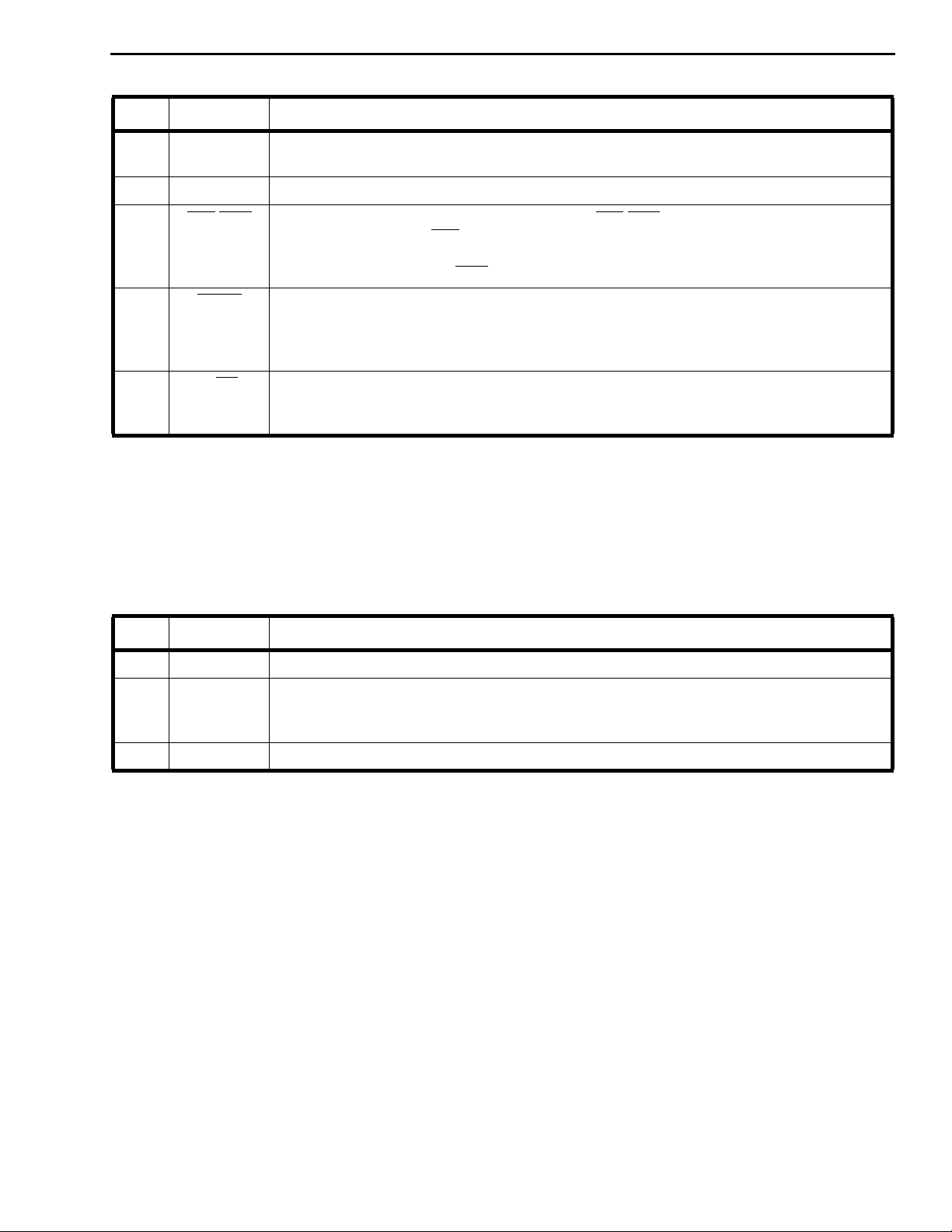
BIT NAME DESCRIPTION
B7 NA A ‘1’ will allow access to Control Register 1 and Master Status Register.
A ‘0’ will prevent it.
B6-B3 NA
B2 IRQ/NDA The state of this pin will select the mode of the IRQ/NDA pin.
B1 M/Sen A ’0’ will enable the transmission of the M
B0 P/SC The Parallel/Serial Control bit selects the source of the control channel. If ’0’, then the
Note 1: These bits have no designated memory space and will read as the last values written to the microprocessor por t.
Note 2: The transmission of M=1 is used for a second level of multiframing.
(1)
Keep at ’0’ for normal operation.
A ’0’ will enable the IRQ pin for HDLC interrupts.
A ’1’ will enable the New Data Available signal which identifies the access time to the
synchronous registers. (If NDA is enabled, the HDLC interrupts are disabled.)
(2)
or S bit as selected in the NT Mode C-channel
Register (refer to Table 13). The selection of M or S is determined by the HALF signal
(refer to functional timing).
A ’1’ will disable this feature forcing the M and S bits to binary zero.
C-channel Register is access through the ST-BUS stream. If ’1’, then the C-channel
Register is accessed through the microprocessor port.
Table 3. Master Control Register (Read/Write Add. 00000B)
BIT NAME DESCRIPTION
B7 NA Keep at ‘0’ for normal operation.
B6 RxDIS When set to ‘1’, this bit disables the S-Bus signal receiver. It can be used, for example, to
force INFO4 to INFO2 transition in the NT state machine while receiving INFO3 from the
TE.
B5-B0 NA Keep at ‘0’ for normal operation.
Table 4. Control Register 1 (Write Add. 10000B)
9-87
Page 18

MT8931C
BIT NAME DESCRIPTION
B7 CH3i
B6 CH2i
B5 CH1i
B4 CH0i
B3 CH3o
B2 CH2o
B1 CH1o
B0 CH0o
Note 3: All ST-BUS channels are enabled in controllerless mode.
(3)
If ’1’, then the ST-BUS channel 3 input port is enabled (B2-channel).
If ’0’, then the channel is disabled, and will read FFH.
(3)
If ’1’, then the ST-BUS channel 2 input port is enabled (B1-channel).
If ’0’, then the channel is disabled, and will read FFH.
(3)
If ’1’, then the ST-BUS channel 1 input port is enabled (C-channel).
If ’0’, then the channel is disabled, and will read 00H.
(3)
If ’1’, then the ST-BUS channel 0 input port is enabled (D-channel).
If ’0’, then the channel is disabled, and will read FFH.
(3)
If ’1’, then the ST-BUS channel 3 output port is enabled (B2-channel).
If ’0’, then the channel is disabled and it will be placed in High impedance.
(3)
If ’1’, then the ST-BUS channel 2 output port is enabled (B1-channel).
If ’0’, then the channel is disabled and it will be placed in High impedance.
(3)
If ’1’, then the ST-BUS channel 1 output port is enabled (C-channel).
If ’0’, then the channel is disabled and it will be placed in High impedance
(3)
If ’1’, then the ST-BUS channel 0 output port is enabled (D-channel).
If ’0’, then the channel is disabled and it will be placed in High impedance.
Table 5. ST-BUS Control Register (Read/Write Add. 00001B)
BIT NAME DESCRIPTION
B7 TxEn A ’1’ enables the HDLC transmitter for the selected D-channel (i.e., ST-BUS or S-Bus).
A ’0’ disables the HDLC transmitter (i.e., an all 1s signal will be sent).
B6 RxEn A ’1’ enables the HDLC receiver for the selected D-channel (i.e., ST-BUS or S-Bus).
A ’0’ disables the HDLC receiver (i.e., an all 1s signal will be received).
B5 ADRec If ’1’, then the address recognition is enabled. This forces the receiver to recognize only
those packets having the unique address as programmed in the Receive Address
Registers or if the address byte is the All-Call address (all 1s).
If ’0’, then the address recognition is disabled and every valid packet is stored in the
received FIFO.
B4 TxPrtSel This bit selects the port of the HDLC transmitted D-channel.
A’1’ selects the S-Bus port. A ’0’ selects the ST-BUS port.
B3 RxPrtSel This bit selects the port of the HDLC received D-channel.
A ’1’ selects the S-Bus port. A ’0’ selects the ST-BUS port.
B2 IFTF This bit selects the Inter Frame Time Fill.
A ’1’ selects continuous flags. A ’0’ selects an all 1’s idle state.
B1 NA Keep at ’0’ for normal operation.
B0 HLoop A ’1’ will activate the HDLC loopback where the transmitted D-channel is looped back to
the received D-channel
(1)
. In NT mode, the transmission of the packet is not affected. In
TE mode, however, the DReq bit of the C-channel Control Register must be set to ‘1’ for
the packet to be transmitted to the S-Bus.
A ’0’ disables the loopback.
Table 6. HDLC Control Register 1 (Read/Write Add. 00010B)
Note 1: The HDLC receiver must be enabled as well as the designated channel.
9-88
Page 19

MT8931C
BIT NAME DESCRIPTION
B7-B5 NA Keep at ’0’ for normal operation.
B4 Trans A ’1’ will place the HDLC in a transparent mode. This will perform the serial to parallel
or parallel to serial conversion without inserting or deleting the opening and closing
flags, CRC bytes or zero insertion. The source or destination of the data is determined
by the port selection bits in the HDLC Control Register 1.
B3 RxRst A transition from ‘0’ to ’1’ will reset the receive FIFO. This causes the receiver to be
disabled until the reception of the next flag. (The status Register will identify the
RxFIFO as being empty.) The device resets this bit to ‘0’ immediately after clearing the
receive FIFO.
B2 TxRst A transition from ‘0’ to ’1’ will reset the transmit FIFO. This causes the transmitter to
clear all data in the TxFIFO. The de vice resets this bit to ‘0’ immediately after clearing
the transmit FIFO.
B1 FA
B0 EOP
Note 2: These bits will be reset after a write to the TxFIFO
(2)
(2)
A ’1’ will ’tag’ the next byte written to the transmit FIFO and cause an abort sequence to
be transmitted once it reaches the bottom of the FIFO.
A ’1’ will ’tag’ the next byte written to the transmit FIFO and cause an end of packet
sequence to be transmitted once it reaches the bottom of the FIFO.
Table 7. HDLC Control Register 2 (Write Add. 00011B)
BIT NAME DESCRIPTION
B7-B6 RxByte
Status
B5-B4 RxFIFO
Status
B3-B2 TxFIFO
Status
B1 Idle If ’1’, an idle channel state has been detected.
These two bits indicate the status of the received byte which is ready to be read from the
19 deep received FIFO. The status is encoded as follows:
B7 - B6
0 - 0 - Packet Byte
0 - 1 - First Byte
1 - 0 - Last Byte (Good FCS)
1 - 1 - Last Byte (Bad FCS)
These two bits indicate the status of the 19 deep receive FIFO . This status is encoded as
follows:
B5 - B4
0 - 0 - Rx FIFO Empty
0 - 1 - ≤14 Bytes
1 - 0 - Rx FIFO Overflow
1 - 1 - ≥15 Bytes
These two bits indicate the status of the 19 deep transmit FIFO as follows:
B3 - B2
0 - 0 - Tx FIFO Full
0 - 1 - ≥5 Bytes
1 - 0 - Tx FIFO Empty
1 - 1 - ≤4 Bytes
B0 Int If ’1’ an unmasked asynchronous interrupt has been detected.
Figure 8. HDLC Status Register (Read Add. 00011B)
9-89
Page 20

MT8931C
BIT NAME DESCRIPTION
B7 EnDcoll A ’1’ will enable the D-channel collision interrupt.
A ’0’ will disable it. This bit is available only in TE mode.
B6 EnEOPD A ’1’ will enable the received End of Packet interrupt.
A ’0’ will disable it.
B5 EnTEOP A ’1’ will enable the transmit End of Packet interrupt.
A ’0’ will disable it.
B4 EnFA A ’1’ will enable the Frame Abort interrupt.
A ’0’ will disable it.
B3 EnTxFL A ’1’ will enable the Transmit FIFO Low interrupt.
A ’0’ will disable it.
B2 EnTxFun A ’1’ will enable the Transmit FIFO Underrun interrupt.
A ’0’ will disable it.
B1 EnRxFF A ’1’ will enable the Receive FIFO Full interrupt.
A ’0’ will disable it.
B0 EnRxFov A ’1’ will enable the Receive FIFO Overflow interrupt.
A ’0’ will disable it.
Table 9. HDLC Interrupt Mask Register (Write Add. 00100B)
BIT NAME DESCRIPTION
B7 Dcoll
(1)
A ’1’ indicates that a collision has been detected on the D-channel (i.e., received E-bit
does not match with transmitted D-bit). This bit is availab le only in TE mode and when the
HDLC transmitter is enabled. It always reads ’0’ in NT mode.
B6 EOPD
(1)
A ’1’indicates that an end of packet has been detected on the HDLC receiv er . This can be
in the form of a flag, an abort sequence or as an invalid packet.
B5 TEOP
(1)
A ’1’ indicates that the transmitter has finished sending the closing flag of the last packet in
the Tx FIFO, and the internal priority level is reduced from high to low.
B4 FA
(1)
A ’1’ indicates that the receiver has detected a frame abort sequence on the received data
stream.
B3 TxFL
(1)
A ’1’ indicates that the device has only four Bytes remaining in the Tx FIFO. This bit has
significance only when the Tx FIFO is being depleted and not when it is getting loaded.
B2 TxFun
(1)
A ’1’ indicates that the Tx FIFO is empty without being given the ’end of packet’ indication.
The HDLC will transmit an abort sequence after encountering an underrun condition.
B1 RxFF
(1)
A ’1’ indicates that the HDLC controller has accumulated at least 15 bytes in the Rx
FIFO.
B0 RxFov
(1)
A ’1’ indicates that the Rx FIFO has overflown (i.e., an attempt to write to a full Rx FIFO).
The HDLC will always disable the receiver once the receive overflow has been detected.
The receiver will be re-enabled upon detection of the next flag.
Table 10. HDLC Interrupt Status Register (Read Add. 00100B)
Note 1: All interr upts will be reset after a read to the HDLC Interrupt Status Register.
9-90
Page 21

MT8931C
BIT NAME DESCRIPTION
B7-B2 R1A7-R1A2 A six bit mask used to interrogate the first byte of the received address (where B7 is MSB).
If address recognition is enabled, any packet failing the address comparison will not be
stored in the Rx FIFO.
B1 NA Not applicable to address recognition.
B0 A1En If ’0’, the first byte of the address field will not be used during address recognition.
If ’1’ and the address recognition is enabled, the six most significant bits of the first
address byte will be compared with the first six bits of this register.
Table 11. HDLC Address Recognition Register 1 (Read/Write Add. 00110B)
BIT NAME DESCRIPTION
B7-B1 R2A7-R2A1 A seven bit mask used to interrogate the second byte of the received address (where B7
is MSB). If address recognition is enabled, any pack et failing the address comparison will
not be stored in the Rx FIFO. This mask is ignored if the address is a Broadcast (i.e., R2A
= 1111111).
B0 A2En If ’0’, the second byte of the address field will not be used during address recognition.
If ’1’ and the address recognition is enabled, the seven most significant bits of the second
address byte will be compared with the first seven bits of this register.
Table 12. HDLC Address Recognition Register 2 (Read/Write Add. 00111B)
BIT NAME DESCRIPTION
B7 AR Setting this bit will initiate the activation of the S-Bus.
If ’0’, the device will remain in the present state.
B6 DR Setting this bit will initiate the deactivation of the S-Bus.
If ’0’, the device will remain in the present state. This bit has priority over AR.
B5 DinB If ’1’, the D-channel will be placed in the B1 timeslot allocating 64 kbit/s to the
D-channel.
(1)
If ’0’, the D-channel will assume its position with a 16 kbit/s bandwidth.(1)
B4 Timing A ’0’ will set the NT in a short passive bus configuration using a fixed timing source (no
compensation for line length).
A ’1’ will set the NT in a point-to-point or extended passive b us configur ation with adaptiv e
timing compensation.
B3 M/S This bit represents the state of the transmitted M/S-bit. M when HALF=0 and S when
HALF=1.
B2 HALF The state of this bit identifies which half of the frame will be transmitted on the
S-Bus. The operation of this signal is similar to that of the HALF pin.
B1 TxMFR A ’1’ in this bit, while HALF = 0, will force the transmission of a m ultiframe sequence in the
Fa and N bits, i.e., Fa=1 and N=0. A ‘0’ will resume normal operation, i.e., Fa=0 and N=1.
B0 RegSel If the register select bit is set to ’1’, the control register is redefined as the diagnostic
register. A ’0’ give access to the control register.
Table 13. NT Mode C-channel Control Register
Note 1: Allow one ST-BUS frame to input the C-channel and one ST-BUS frame to establish the connection.
Note 2: The C-channel Control Register is updated once every ST-BUS frame. Therefore, this register should not be written to
more than once per frame, otherwise, the last access will override previous ones.
(2)
(Write Add. 01000B and B0 = 0)
9-91
Page 22

MT8931C
BIT NAME DESCRIPTION
B7-B6 Loop The status of these two bits determine which type of loopback is to be performed:
B7 - B6
0 - 0 - no loopback active
0 - 1 - near end loopback LTx to LRx
1 - 0 - digital loopback DSTi to DSTo
1 - 1 - remote loopback LRx to LTx
B5 FSync If ’1’, the device will maintain frame synchronization even after losing the frame sync
sequence (i.e., if the device is transmitting INFO2 or INFO4 and this bit is set, the same
INFO signal will still be transmitted even if the fr ame sync sequence in the received signal
is lost).
If ’0’, synchronization will be declared when three consecutive framing sequences have
been detected without error.
B4 FLv If ’1’, the frame sync sequence will violate the bipolar violation encoding rule.
If ’0’, the framing pattern resumes normal operation, i.e., Framing bit is a bipolar violation.
B3 Idle Setting this bit to ’1’ will force an all 1s signal to be transmitted on the line.
B2 Echo Setting this bit to ’1’ will force all D-echo bits (E) to zero.
B1 Slave If ’1’, the device will operate in a NT slave mode. This allows the device to be used at the
terminal equipment end of the line while receiving its clocks from an external source.
B0 RegSel If the register select bit is set to ’1’, the control register is redefined as the diagnostic
register. A ’0’ gives access to the control register.
Table 14. NT Mode C-channel Diagnostic Register (Write Add. 01000B and B0 = 1)
BIT NAME DESCRIPTION
B7 Sync/BA This bit is set when the device has achieved frame synchronization while the activation
request is asserted (DR = 0 and AR = 1). If there is a deactivation request or AR is low
(DR = 1 or AR = 0), this bit indicates the presence of bus activity
(1)
. A bus activity
identifies the reception of INFO frames (INFO1 or INFO3).
B6-B5 IS0-IS1 Binary encoded state sequence.
IS0 - IS1
0 - 0 - deactivated
0 - 1 - pending deactivation
1 - 0 - pending activation
1 - 1 - activated
B4 RxMCH Following a ‘0’ input at the HALF pin or HALF bit in the C-channel Control Register, the
state of this bit reflects the received maintenance Q-channel (received in the Fa bit
position during multiframing).
This bit will always read ‘1’ if multiframing is not used.
B3-B0 NA These bits will read ’1’.
Table 15. NT Mode Status Register
Note 1: Bus activity is set when three zeros are received in a time period equivalent to 48 bits or 250µs. It is reset when 128
consecutive ones are received.
Note 2: The Status Register is updated internally once every ST-BUS frame. Therefore, more than one read access per frame will
return the same value.
(2)
(Read Add. 01001B)
9-92
Page 23

BIT NAME DESCRIPTION
B7 AR Setting this bit will initiate the activation of the S-Bus.
If ’0’, the device will remain in the present state.
B6 DR Setting this bit will initiate the deactivation of the S-Bus.
If ’0’, the device will remain in the present state. This bit has priority over AR.
MT8931C
B5 DinB If ’1’, the D-channel will be placed in the B1 timeslot allocating 64 kbit/s to the
D-channel.
If ’0’, the D-channel will assume its position with a 16 kbit/s bandwidth.
(1)
(1)
B4 Priority The status of this bit selects the priority class of the terminal equipment. A ’1’ selects the
high priority and a ’0’ selects the low priority.
B3 DReq This bit is used to request or relinquish the D-channel on the S-Bus when the D-channel
source is the ST-BUS. A ’1’ will request the D-channel, a ’0’ will relinquish it.
Keep at ’0’ when the D-channel source is the HDLC transmitter.
B2 TxMCH The state of this bit will be transmitted in the maintenance channel (Q-channel).
B1 ClrDia A ’1’ will clear the contents of the Diagnostics Register.
A ’0’ will enable the maintenance functions found in the Diagnostic Register.
This bit should be set to 1 as long as the device is not fully active (IS0, IS1 ≠ 1,1).
B0 RegSel If the register select bit is set to ’1’, the control register is redefined as the diagnostic
Register. A ’0’ gives access to the Control Register.
Table 16. TE Mode C-channel Control Register
Note 1: Allow one ST-BUS frame to input the C-channel and one ST-BUS frame to establish the connection.
Note 2: The C-channel Control Register is updated once every ST-BUS frame. Therefore, this register should not be written to
more than once per frame, otherwise, the last access will override previous ones.
(2)
(Write Add. 01000B and B0 = 0)
BIT NAME DESCRIPTION
B7-B6 Loop The status of these two bits determine which type of loopback is to be performed:
B7 - B6
0 - 0 - no loopback active
0 - 1 - near end loopback LTx to LRx
1 - 0 - digital loopback DSTi to DSTo
1 - 1 - remote loopback LRx to LTx
B5 FSync If ’1’, the device will maintain frame synchronization even after losing the frame sync
sequence (i.e., if the device is transmitting INFO3 and this bit is set, INFO3 will still be
transmitted even if the frame sync sequence in the received signal is lost).
If ’0’, synchronization will be declared when three consecutive framing sequences have
been detected.
B4 FLv If ’1’, the frame sync sequence will violate the normal bipolar encoding rule.
If ’0’, the framing pattern resumes normal operation, i.e., framing bit will be a bipolar
violation.
B3 Idle If ’1’, an all 1s signal is transmitted on the line.
If ’0’, the transmitter will resume normal operation.
B2-B1 NA Unused.
B0 RegSel If the register select bit is set to ’1’, the control register is redefined as the diagnostic
register. A ’0’ gives access to the control register.
Table 17. TE Mode Diagnostic Register (Write Add. 01000B and B0 = 1)
9-93
Page 24

MT8931C
BIT NAME DESCRIPTION
B7 Sync/BA This bit is set if the device has achieved frame synchronization while the activation
request is asserted (DR = 0 and AR = 1). If there is a deactivation request or that AR is
low (DR = 1 or AR = 0), this pin indicates the presence of bus activity
identifies the reception of INFO frames (INFO2 or INFO4).
B6-B5 IS0-IS1 Binary encoded state sequence.
IS0 - IS1
0 - 0 - deactivated
0 - 1 - synchronized
1 - 0 - activation request
1 - 1 - activated
B4 M/S This bit respresents the state of the received M/S-bit. M when HALF=0 and S when
HALF=1
B3 HALF The state of this bit identifies which half of the S-Bus frame is currently being output on the
ST-BUS.
B2 RxMFR A ’1’ when HALF=0 indicates that the multiframe pattern on Fa and N has been detected.
B1 Priority The status of this bit indicates the internal priority of the device within the designated
priority class. If 1, then it has high priority within the priority class designated in B4 of
control register. If 0, then it has low priority within the priority class designated in B4 of
control register.
(1)
. A bus activity
B0 DCack A ’1’ indicates that the device has gained access to the D-channel and has transmitted an
opening flag. This bit is reset to ‘0’ when the closing flag of the last packet in the TxFIFO
is transmitted and the internal priority is reduced from high to low. A collision during
transmission will also reset this bit back to ‘0’.
Table 18. TE Mode Status Register
Note 1: Bus activity is set when three zeros are received in a time period equivalent to 48 bits or 250µs. It is reset when 128
Note 2: The Status Register is updated internally once every ST-BUS frame. Therefore, more than one read access per frame will
consecutive ones are received.
return the same value.
(2)
(Read Add. 01001B)
BIT NAME DESCRIPTION
B7-B2 NA Not available.
B1* INFO1 In TE mode, this bit is set to ‘1’ only when the device is transmitting INFO1.
Not available in NT mode.
B0* INFO0 In NT or TE mode, this bit is set to ‘1’ only when the device is transmitting INFO0.
Table 19. Master Status Register (Read Add. 10010B)
* These two bits can be used along with status bits IS0 and IS1 to distinguish between states F6/F8 and F4/F5 of the device’s state machine in
TE mode. Please refer to “State Machine” section of Application Note MSAN-141 for further details.
9-94
Page 25
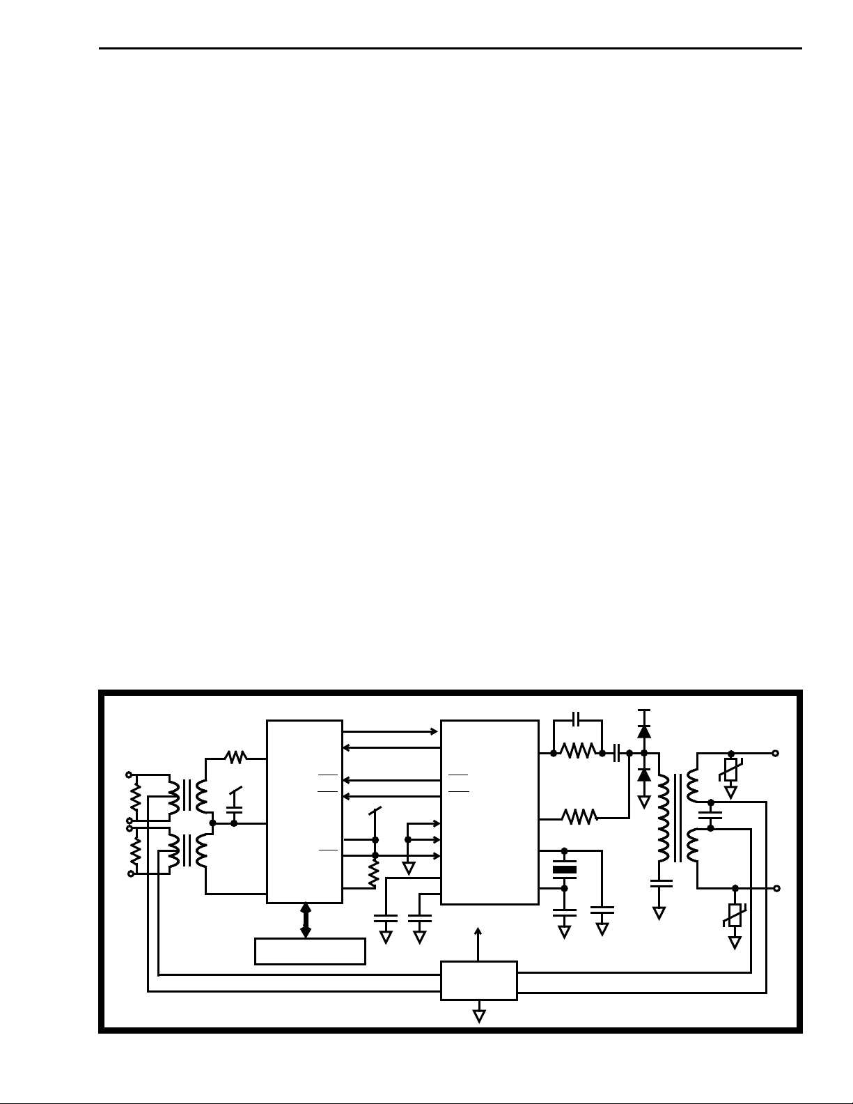
MT8931C
Applications
The MT8931C is useful in a wide variety of ISDN
applications. Being used at both the Network
Termination (NT) and Terminal Equipment (TE) ends
of the line, the SNIC finds application on digital
subscriber line cards and in full featured digital
telephone sets.
The SNIC can be combined with the MT8971B/72B
to implement an NT1 function(with biphase line code
on the U interface) as shown in Figure 16. It can
also be combined with the MT8910 to implement an
ISDN NT1 function (with 2B1Q line code on the U
interface) as shown in Figure 17. The MT8931C is
configured in NT mode, acting as a master to the Sinterface line, while the MT8971B/72B or the
MT8910 operates in slave mode and derives its
timing from the U-interface line originating from the
central office.
Figure 18 illustrates the use of the SNIC in
conjunction with the MT9094 to implement a 2B+
D, ISDN telephone set. The MT9094 provides such
features as A/D and D/A conversion, handset
interface, handsfree operation and tone ringer. PCM
encoded voice is passed from the MT9094 to the
SNIC via the ST-BUS por t for transmission on one of
the B-channels. The second B-channel is available
for transmission of data. These two devices have
been designed to connect together with virtually no
interconnection components.
features and control functions. Signalling may be
performed by scanning the keypad and generating
appropriate messages to be packetized by the HDLC
section of the SNIC and transmitted via the Dchannel. A twelve segment, non-multiplexed LCD
display can be connected directly to the S12-S1
outputs to provide various status and call progress
indicators.
It must be noted, that the pseudo-ternary line code
will tolerate line rev ersals within the LRx and LTx pair
between the NT and TE. However, re v ersal of the TE
transmit pair between two or more TEs will make the
S-interface inoperable.
In multidrop applications, a powered-off TE must not
load the line and prevent communications between
the NT and other TEs. To avoid such a situation, one
mechanical relay should be used to disconnect the
LTx pin and the LRx pin from the line transformers.
Interfacing to Non-Multiplexed Busses
The microprocessor interface for the SNIC was
designed around a multiplexed bus architecture
which may be found with most Intel processors/
controllers or a few Motorola processors. In the
event that your choice of processors is restricted, a
simple application circuit can convert the nonmultiplexed bussing to that of a multiplexed
architecture. Figure 19 provides an to interface the
MC6802 or the MC6809 microprocessors.
Both the MT8931C and MT9094 are controlled and
monitored by a microprocessor to implement various
MT8931C MT8971B/72B
R
Tx
1:2*
‡
R
‡
R
+5V
10µF
1:2*
DSTo
LTx
LRx
Microprocessor
DSTi
F0b
C4b
V
Bias
NT
Rsti
Star
+5V
10kΩ
0.33µF
Figure 16 - NT1 Function
DSTi
DSTo
F0b
C4b
MS0
MS1
MS2
V
REF
V
Bias
0.33µF
DC to DC
Converter
+5V
L
OUT
L
OSC1
OSC2
IN
10.24 MHz XTAL
33 pF
1.5 nF
390 Ω
47 Ω
22 nF
33 pF
0.33 µF
+5V
2:1
‡
100Ω terminating resistor
1.0 µF
9-95
Page 26
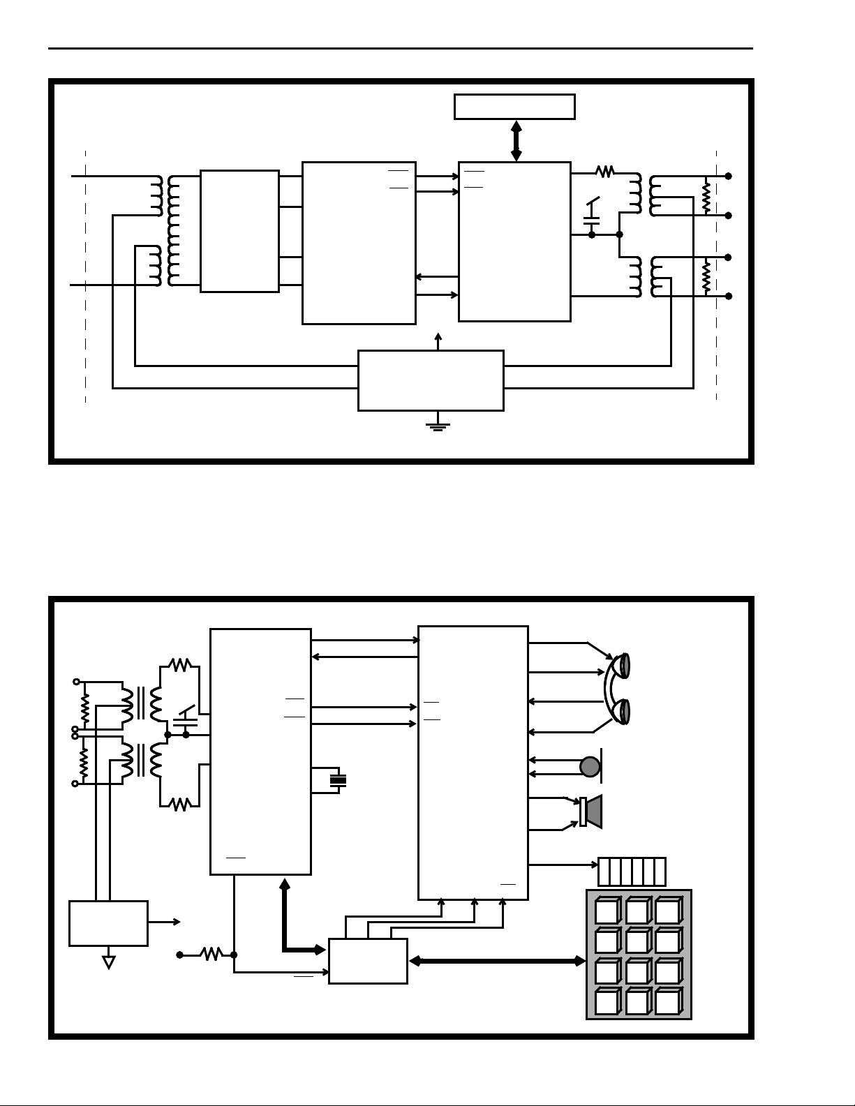
MT8931C
Microprocessor
U Reference
Point
Termination
Network
MH89101
L
out+
L
in+
L
in-
L
out-
MT8910-1
DSLIC
C4b
F0b
DSTi
DSTo
C4b
F0b
DSTo
DSTi
MT8931C
NT Mode
LTx
V
Bias
LRx
R
Tx
V
DD
10µF
+5V
Power Supply
and
Power Feed
‡
100Ω terminating resistor
Figure 17 - NT1 using the MT8910-1 (DSLIC) and MT8931C (SNIC)
2:1
2:1
R
R
S Reference
Point
‡
‡
‡
R
‡
R
DC to DC
Converter
‡
MT8931C
R
Tx
1:2
V
DD
LTx
V
Bias
LRx
1:2
2kΩ
IRQ
+5V
+5V
10k
100Ω terminating resistor
DSTo
DSTi
F0b
C4b
XTAL1
XTAL2
Data Port
IRQ
8051
DSTi
DSTo
F0i
C4i
DATA1
MT9094
HSPKR+
HSPKR-
SPKR+
SPKR-
SCLK
M+
M-
MIC+
MIC-
S12-1
CS
Handset
Microphone
Speaker
Display
23
1
456
789
#
0
*
K
e
y
p
a
d
9-96
Figure 18 - ISDN Digital Telephone Set
Page 27
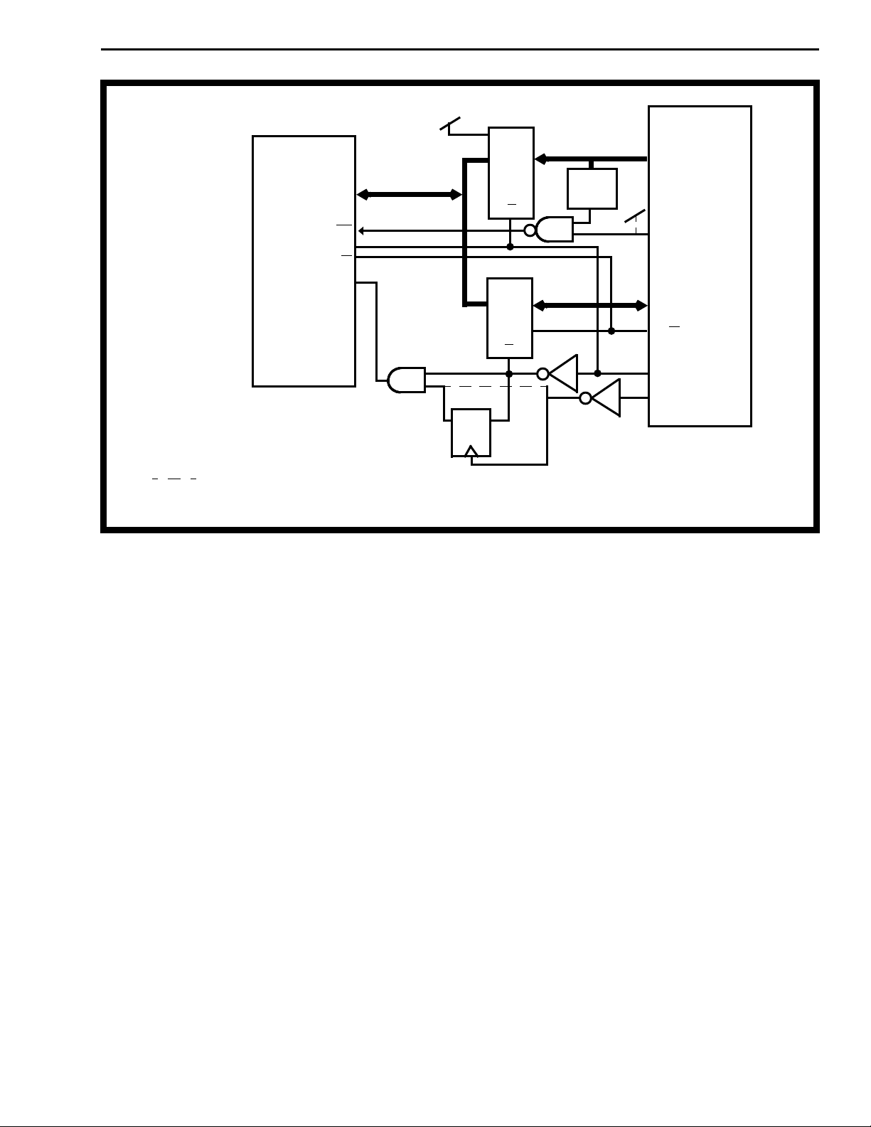
MT8931C
MT8931C
AD0-AD7
CS
DS
R/
W
AS
Connections to interface to MC6809
V
DD
74HCT245
74HCT245
QD
DIR
B
A
G
G
A
B
DIR
Address
Decoder
V
DD
MC6802
(MC6809)
A0 - A7
VMA
D0 - D7
W
R/
E
EXTAL (Q)
Figure 19 - Interfacing to the MC6802 Microprocessor
TS 300-012 NT&TE Line Interface
Figures 20, 21 and 22 show the recommended line
interface circuits for meeting the ETS 300-012
requirements. These circuits assume that test
measurements are made using the "standard
reference cord" which has the following
specifications:
C = 315pF to 350pF
R = 2.7Ω to 3.0Ω
Z > 75Ω
Length < 10m
Several types of transformers can be used:
• Filtran TPW-3852-4 (Figure 20)
• VAC T60403-L4096-X028 (Breakdown Voltage
4KV) (Figure 21)
• VAC T60403-L4096-X027 Breakdown Voltage
2KV) (Figure 21)
• VAC T60403-L4096-X029 (Breakdown Voltage
4KV) (Figure 22)
• VAC T60403-L4096-X030 (Breakdown Voltage
2KV) (Figure 22)
L4096-X029 and L4096-X030 are equivalent to
L4096-X028 and L4096-X027 with the exceptions of
pin out; L4096-X029 and L4096-X030 are pin
compatible with L4096-X028-80.
In Figure 20, T1, 2 (Filtran TPW-3852-4) provides
isolation, longitudinal balance, impedance matching
and voltage level conversion. D5 and 6 (germanium)
ensure that the pulse shape lies within the center of
the various pulse templates. D1-4 protect the
MT8931C from line transients. C2, 3 decouple the
VBias voltage and optimize the receiver sensitivity.
R1 and C4 make up a low-pass filter recommended
for delaying the signal in TE applications, this filter
can also be used for NT applications allowing
common hardware for TE and NT applications. K1
isolates the MT8931C from the line for multidrop
applications in cases where the device is powered
down. L1 is 4-winding 5mH common mode choke to
suppress EMI on the 4-wire line.
The TPW-3852-4 is available from:
Filtran Ltd.
229 Colonnade Road
Nepean, Ontario
Canada
Telephone: (613) 226-1626
9-97
Page 28
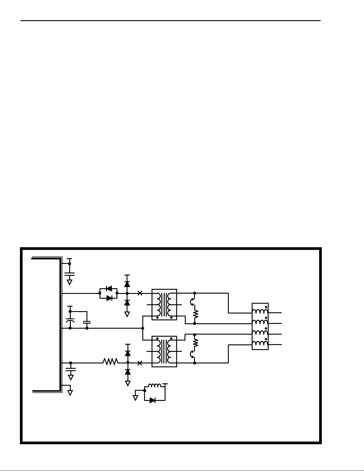
MT8931C
In Figure 21, two types of diodes (germanium 1N270
or schottky MBD301) can be used for D5,6. 1N270
will leave more margin for pulse template and
longitudinal conversion loss. However, MBD301 will
leave more margin for impedance template. All other
components are as described previously for Figure
20.
The VAC Transformers are available from:
Germany
Vacuumschmelze GMBH
Postfach 22 53
D-63412 Hanau
Telephone: (49) 6181 380
Canada
Votron Electronic Ltd.
250 Rayette Road
Concord, Ontario L4K 2G6
Telephone: (905) 669-9870
Proprietary NT&TE Line Interface
For proprietary applications, where stringent
requirements such as ETS 300-012 do not have to
be met, the line interface circuit may be simpler and
consequently less expensive. Figure 23 shows such
a line interface circuit. R1 should be chosen
according to the transformer selected and the
desired output signal level, typical values of R1 may
vary from 30Ω to 75Ω. Numerous types of
transformers may be used, including the following:
APC 8016D (dual with common mode choke)
Filtran TEW-5660 (surface mount)
Filtran TPW-3852-4 (single)
Pulse PE-65495 (dual)
VAC L4097-X028-80 (single)
In Figure 22, everything is the same as in Figure 21,
except transformer pin out.
USA
Vacuumschmelze Corporation
4027 Will Rogers Parkway
Oklahoma City, OK 73108
Telephone: (405) 943-9651
V
DD
V
DD
MT8931C
LTx
V
LRx
V
Bias
SS
C1
V
DD
+
C2
C3
C4
V
DD
D5
D6
R1
D1
D2
V
DD
D3
D4
T1
5
K1
4
3
T2
3
4
5
K1
V
K1
D7
DD
6
1
2
2
1
6
R2
R3
L1
6
7
9
10
5
Tx+
4
Tx-
2
Rx-
1
Rx+
Parts List:
C1, 3 = 0.1µF Ceramic
C2 = 10µF Tantalum
C4 = 22pF
D1-4 = IN914
D5, 6 = IN270 Germanium
D7 = IN4003
K1 = 2 Form A or C Relay
(eg., Aromat TQ2E-5V)
L1 = VAC N4025-X034
R1 = 3k01 1%
R2, 3 = 100Ω 1%
T1, 2 = Filtran TPW-3852-4
9-98
Figure 20 - ETS 300-012 NT & TE Line Interface for Filtran TPW-3852-4
Page 29
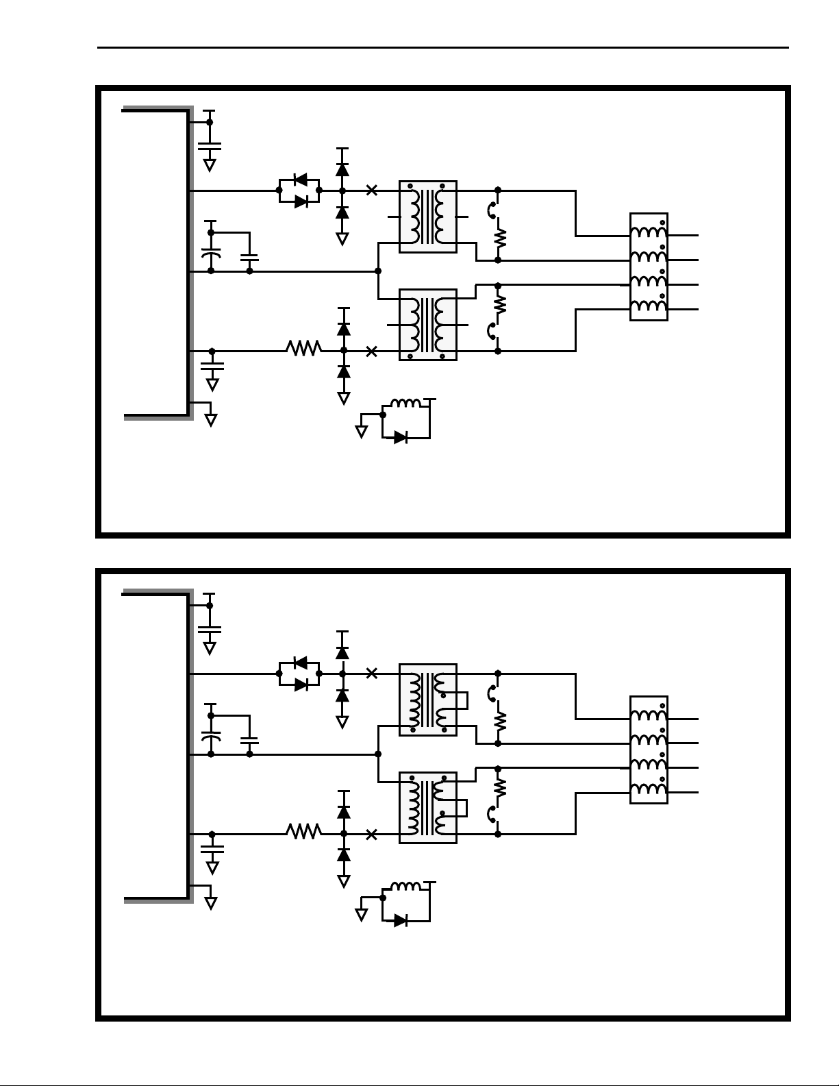
MT8931C
V
LTx
V
LRx
Bias
V
DD
SS
MT8931C
V
DD
V
C1
D5
V
DD
+
C2
C4
D6
C3
DD
D1
D2
V
DD
R1
D3
D4
T1
1
K1
2
3
T2
3
2
1
K1
V
K1
DD
4
5
6
6
5
4
R2
R3
L1
6
7
9
10
5
4
2
1
Parts List:
C1, 3 = 0.1µF Ceramic
Tx+
Tx-
Rx-
Rx+
C2 = 10µF Tantalum
C4 = 22pF
D1-4 = IN914
D5, 6 = IN270 Germanium or
MBD301 Schottky
D7 = IN4003
K1 = 2 Form A or C Relay
D7
(Aromat TQ2E-5V)
L1 = VAC N4025-X034
R1 = 3k01 1%
R2,3 = 100Ω 1%
T1, 2 = VAC T60403-L4096-
X027 or VAC T60403-L4096X028
MT8931C
V
LTx
V
LRx
Figure 21 - ETS 300-012 NT & TE Line Interface for VAC X027 or X028
V
DD
Bias
V
DD
SS
C1
V
DD
+
C2
C3
C4
V
DD
D5
D6
R1
D1
D2
V
DD
D3
D4
T1
6
K1
1
T2
1
6
K1
V
K1
D7
DD
4
3
5
2
2
5
3
4
R2
R3
L1
6
7
9
10
5
Tx+
4
Tx-
2
Rx-
1
Rx+
Parts List:
C1, 3 = 0.1µF Ceramic
C2 = 10µF Tantalum
C4 = 22pF
D1-4 = IN914
D5, 6 = IN270 Germanium or
MBD301 Schottky
D7 = IN4003
K1 = 2 Form A or C Relay
(Aromat TQ2E-5V)
L1 = VAC N4025-X034
R1 = 3k01 1%
R2,3 = 100Ω 1%
T1, 2 = VAC T60403-L4096-
X029 or VAC T60403-L4096X030
Figure 22 - ETS 300-012 NT & TE Line Interface for VAC X029 or X030
9-99
Page 30
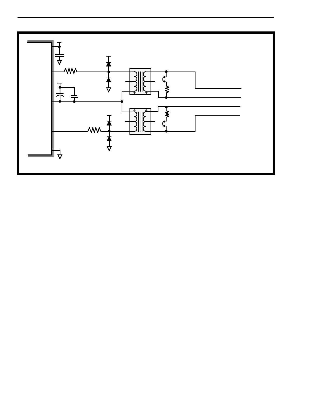
MT8931C
V
DD
MT8931C
LTx
V
Bias
LRx
V
SS
V
DD
V
C1
R1
V
DD
+
C2
C3
R2
DD
D1
D2
V
DD
D3
T1
R3
T2
R4
Tx+
Tx-
Rx-
Rx+
Parts List:
D4
C1, 3 = 0.1µF Ceramic
C2 = 10µF Tantalum
D1-4 = IN914
R1 = see circuit description
R2 = 2k to 4k
R3, 4 = 100Ω
T1, 2 = see circuit description
Figure 23 - Proprietary NT & TE Line Interface
9-100
Page 31

Absolute Maximum Ratings*
Parameters Symbol Min Max Units
1 Supply Voltage V
2 Voltage on any I/O pin V
3 Current on any I/O pin I
4 Storage Temperature T
5 Package Power Dissipation P
* Exceeding these values may cause permanent damage. Functional operation under these conditions is not implied.
DD
I/O
I/O
ST
D
-0.3 7.0 V
-0.3 VDD + 0.3 V
-65 150 °C
MT8931C
20 mA
1000 mW
Recommended Operating Conditions - Voltages are with respect to ground (V
Characteristics Sym Min Typ
1 Supply Voltage V
2 Input High Voltage* V
3 Input Low Voltage* V
4 Load Resistance (LTx) R
5 Load Capacitance (LTx) C
6 Operating Temperature T
‡ Typical figures are at 25
* Except for XTAL1/NT pin. See below.
** Including the transformer DC resistance.
°C and are for design aid only: not guaranteed and not subject to production testing.
4.75 5.0 5.25 V
DD
2.4 V
IH
IL
L
L
OP
0 0.4 V For 400mV noise margin
-40 85 °C
DC Electrical Characteristics - Voltages are with respect to ground (V
‡
Max Units Test Conditions
DD
V For 400mV noise margin
250** Ω With reference to V
32 pF With reference to V
) unless otherwise stated.
SS
) unless otherwise stated.
SS
Characteristics Sym Min Typ‡Max Units Test Conditions
1 Supply Current
NT Activated
NT Deactivated
TE Activated
TE Deactivated
2 Input High Voltage except for pin
I
DDNA
I
DDND
I
DDTA
I
DDTD
V
14
8
16
10
2.0 V Digital inputs
IH
20
11
25
15
mA
mA
mA
mA
Outputs loaded
Outputs unloaded
Outputs loaded
Outputs unloaded
XTAL1/NT
3 Input High Voltage for pin
V
IH
4 V Digital input
XTAL1/NT
4 Input Low Voltage e xcept f or pin
V
IL
0.8 V Digital inputs
XTAL1/NT
5 Input Low Voltage for pin
V
IL
1 V Digital input
XTAL1/NT
6 Output High Current I
7 Output Low Current I
8 Input Leakage (except pin 8) I
OH
OL
iI
10 15 mA VOH=2.4V digital outputs
5 7.5 mA VOL=0.4V digital outputs
10 µAVIN = VSSto V
9 Input Current for pin 8 25 µAVIN = VSSto V
10 Output Leakage High Imped. I
‡ Typical figures are at 25
°C and are for design aid only: not guaranteed and not subject to production testing.
OZ
10 µAV
OUT
= VSSto V
Bias
Bias
DD
DD
DD
AC Electrical Characteristics - Voltages are with respect to ground (V
) unless otherwise stated.
SS
Characteristics Sym Min Typ‡Max Units Test Conditions
1 Input Voltage (LRx) V
2 Input Current (LRx) I
IN
IN
1.5 V Peak with Ref. to V
70 µAVI=1.5Vp Ref. V
@ f=0 - 100 kHz
3 Output Voltage (LTx) V
4 Output Current (LTx) I
5 Input Impedance (LRx) Z
‡ Typical figures are at 25°C and are for design aid only: not guaranteed and not subject to production testing.
O
O
IN
1.5 V Ref. V
7.5 mA VO=1.5Vp Ref. V
20 kΩ f = 100 kHz
, RL=250Ω
Bias
Bias
Bias
, RL=250Ω
Bias
9-101
Page 32
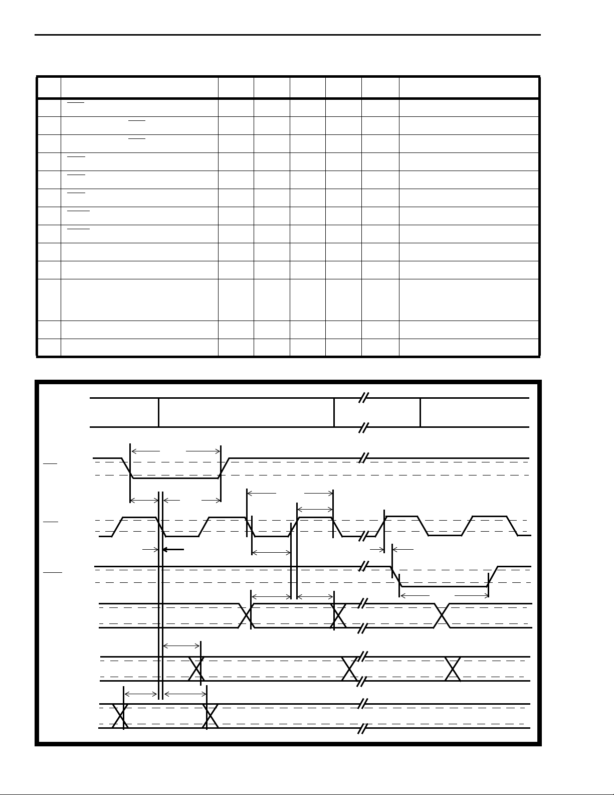
MT8931C
AC Electrical Characteristics† - ST-BUS Timing NT Mode (Ref. Figure 22)
Characteristics Sym Min Typ‡Max Units Test Conditions
1 F0b input pulse width t
2 Frame pulse (F0b) set-up time t
3 Frame pulse (F0b) hold time t
4 C4b input clock period t
5 C4b pulse width High or Low t
6 C4b transition time t
7 F0od delay t
8 F0od pulse width t
9 Serial input set-up time t
10 Serial input hold time t
11 Serial output delay t
FPW
FPS
FPH
P4o
C4W
C4T
DFD
DFW
SIS
SIH
SOD
122 244 ns
35 ns
50 ns
244 ns
122 ns
20 ns
20 87 ns 40 pF Load
244 ns
70 ns
0ns
160
320
ns 50 pF load
50 pF load (HDLC
connected to ST-BUS)
12 HALF input setup time t
13 HALF input hold time t
† Timing is over recommended temperature & power supply voltages
‡ Typical figures are at 25°C and are for design aid only: not guaranteed and not subject to production testing.
HAS
HAH
0ns
200 ns
F0b
C4b
F0od
DSTi
DSTo
ST-BUS Bit Cell
t
FPW
V
IH
V
IL
t
t
t
C4W
SIS
P4o
t
t
C4W
SIH
t
DFD
t
DFW
t
FPS
V
IH
V
IL
V
OH
V
OL
V
IH
V
IL
V
OH
V
OL
t
HAS
t
FPH
t
C4T
t
SOD
t
HAH
HALF
9-102
V
IH
V
IL
Figure 22 - ST-BUS Timing NT Mode
Page 33
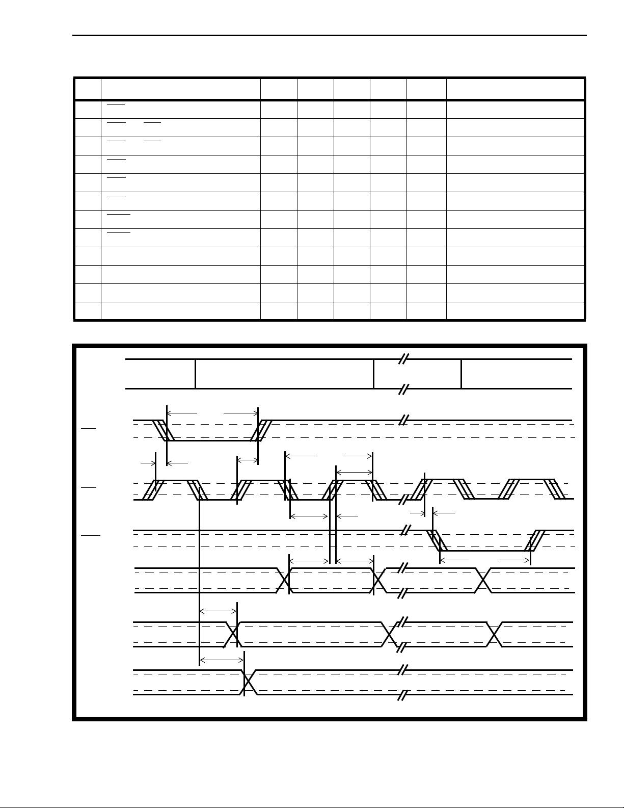
AC Electrical Characteristics† - ST-BUS Timing TE Mode (Ref. Figure 23)
Characteristics Sym Min Typ‡Max Units Test Conditions
MT8931C
1 F0b output pulse width t
2 C4b to (F0b) delay t
3 C4b to (F0b) hold time t
4 C4b output clock period t
5 C4b pulse width High or Low t
6 C4b transition time t
7 F0od delay t
8 F0od pulse width t
9 Serial input setup time t
10 Serial input hold time t
11 Serial output delay t
12 HALF output Delay t
FPW
CFD
CFH
P4o
C4W
C4T
DFD
DFW
SIS
SIH
SOD
HAD
110 122 ns 50 pF load (activated state)
220 244 ns
150 ns
0ns
244 ns 50 pF load
10 50 ns 50 pF load
10 50 ns 50 pF load
244 ns 50 pF load
20 ns 50 pF load
10 50 ns
125 ns 50 pF load
150 ns 50 pF load
† Timing is over recommended temperature & power supply voltages
‡ Typical figures are at 25°C and are for design aid only: not guaranteed and not subject to production testing.
ST-BUS Bit Cell
F0b
C4b
F0od
DSTi
DSTo
HALF
t
FPW
V
OH
V
OL
t
t
SOD
t
CFH
HAD
t
CFD
V
OH
V
OL
V
OH
V
OL
V
IH
V
IL
V
OH
V
OL
V
OH
V
OL
t
t
C4W
SIS
t
P4o
t
C4W
t
t
C4T
t
SIH
DFD
t
DFW
Figure 23 - ST-BUS Timing TE Mode
9-103
Page 34
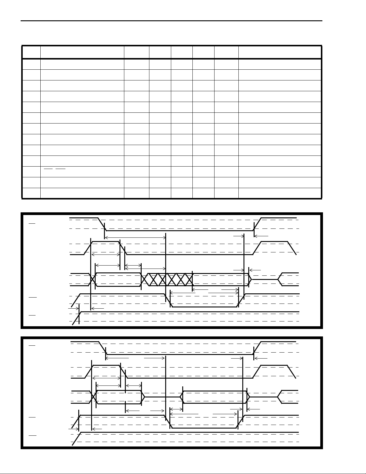
MT8931C
AC Electrical Characteristics† - Intel Bus Interface Timing (Ref. Figure 24 & 25)
Characteristics Sym Min Typ
‡
Max Units Test Conditions
1 Chip select setup time t
2 Chip select hold time t
3 Address Latch pulse width t
4 Address setup time t
5 Address hold time t
6 Data setup time - Write t
7 Data hold time - Write t
8 Data output delay - Read t
9 Data hold time - Read t
10 Write pulse width t
11 RD, WR delay t
12 Read pulse width t
13 Read setup time t
CSS
CSH
ALW
ADS
ADH
DWS
DHW
DOD
DHR
WPW
RWD
RPW
RDS
10 ns
25 ns
50 ns
20 ns
20 ns
35 ns
20 ns
240 ns 50 pF load
25 90 ns 50 pF load
60 ns
60 ns
240 ns
20 ns
† Timing is over recommended temperature & power supply voltages
‡ Typical figures are at 25°C and are for design aid only: not guaranteed and not subject to production testing.
V
IH
CS
ALE
V
IL
t
CSS
V
IH
V
IL
t
t
ALW
ADS
t
ADH
t
RWD
t
CSH
t
DHW
AD0-7
WR
RD
CS
ALE
AD0-7
RD
WR
V
IH
V
IL
V
IH
V
IL
V
IH
V
IL
t
RDS
Address Data in
t
DWS
t
WPW
Figure 24 - Intel Bus Interface Timing (Write Cycle)
V
IH
V
IL
V
IH
V
IL
V
I/OH
V
I/OL
V
IH
V
IL
V
IH
V
IL
t
RDS
t
ALW
t
ADS
Address
t
t
ADH
CSS
t
RWD
t
DOD
Data out
t
RPW
t
CSH
t
DHR
9-104
Figure 25 - Intel Bus Interface Timing (Read Cycle)
Page 35
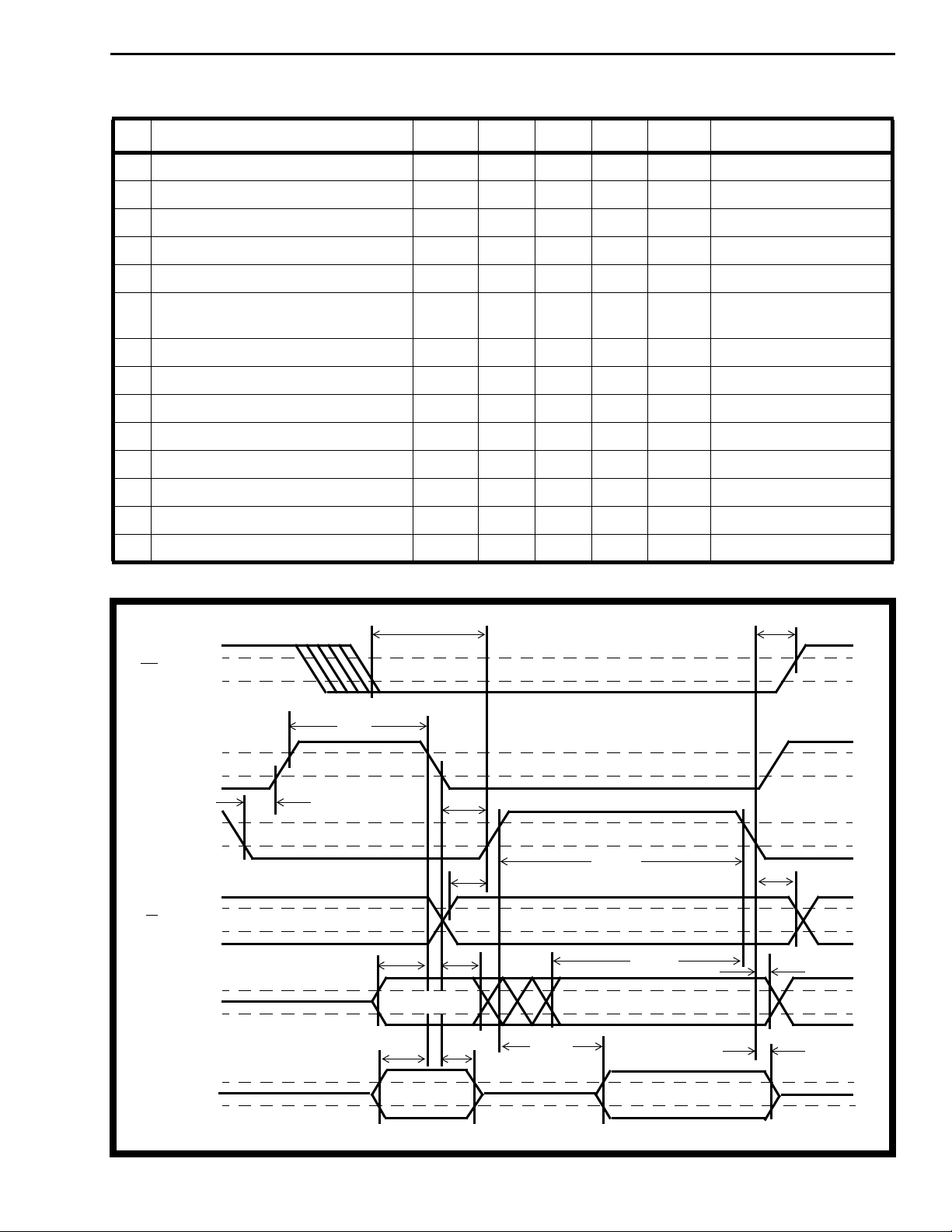
MT8931C
AC Electrical Characteristics†- Motorola Bus Interface Timing (Ref. Figure 26)
Characteristics Sym Min Typ‡Max Units Test Conditions
1 Chip select setup time t
2 Chip select hold time t
3 Address strobe pulse width t
4 Data strobe setup time t
5 Data strobe hold t
6 Data strobe pulse width - Write
CSS
CSH
ASW
DSS
DSH
t
DSW
- Read
7 Read/Write setup time t
8 Read/Write hold time t
9 Address setup time t
10 Address hold time t
11 Data setup time - Write t
12 Data hold time - Write t
13 Data output delay t
14 Data hold time - Read t
† Characteristics are for clocked operation over the ranges of recommended operating temperature and supply voltage.
‡ Typical figures are at 25°C and are for design aid only: not guaranteed and not subject to production testing.
RWS
RWH
ADS
ADH
DWS
DHW
DOD
DHR
10 ns
10 ns
50 ns
20 ns
20 ns
100
240
ns
ns
40 ns
10 ns
20 ns
20 ns
35 ns
30 ns
240 ns 50 pF load
25 90 ns 50 pF load
CS
AS
DS
R/
AD0
-AD7
(Write)
t
CSS
V
IH
V
IL
t
ASW
V
IH
V
IL
t
DSS
V
IH
V
IL
V
W
IH
V
IL
t
ADS
V
IH
V
IL
t
ADS
t
DSH
t
t
RWS
t
ADH
Address Data Input
t
ADH
t
DOD
DSW
t
DWS
t
CSH
t
RWH
t
t
DHR
DHW
AD0
-AD7
(Read)
V
I/OH
V
I/OL
Address Data Output
Figure 26 - Motorola Bus Interface Timing
9-105
Page 36
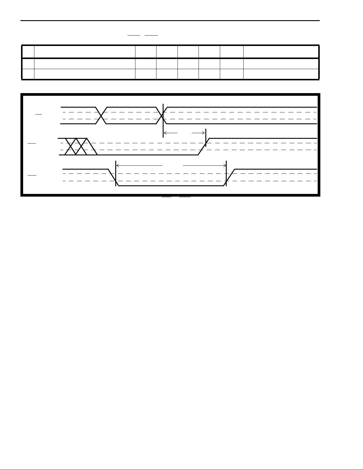
MT8931C
AC Electrical Characteristics†- IRQ, Rsti Timing (Ref. Figure 27)
Characteristics Sym Min Typ‡Max Units Test Conditions
1 Interrupt release delay t
2 Reset pulse width t
† Characteristics are for clocked operation over the ranges of recommended operating temperature and supply voltage.
‡ Typical figures are at 25°C and are for design aid only: not guaranteed and not subject to production testing.
V
DS/RD
IRQ
Rsti
IH
V
IL
V
OH
V
OL
V
IH
V
IL
IRD
RSW
1 µs
100 ns
t
IRD
t
RSW
Figure 27 - INT & Rsti Timing
9-106
Page 37
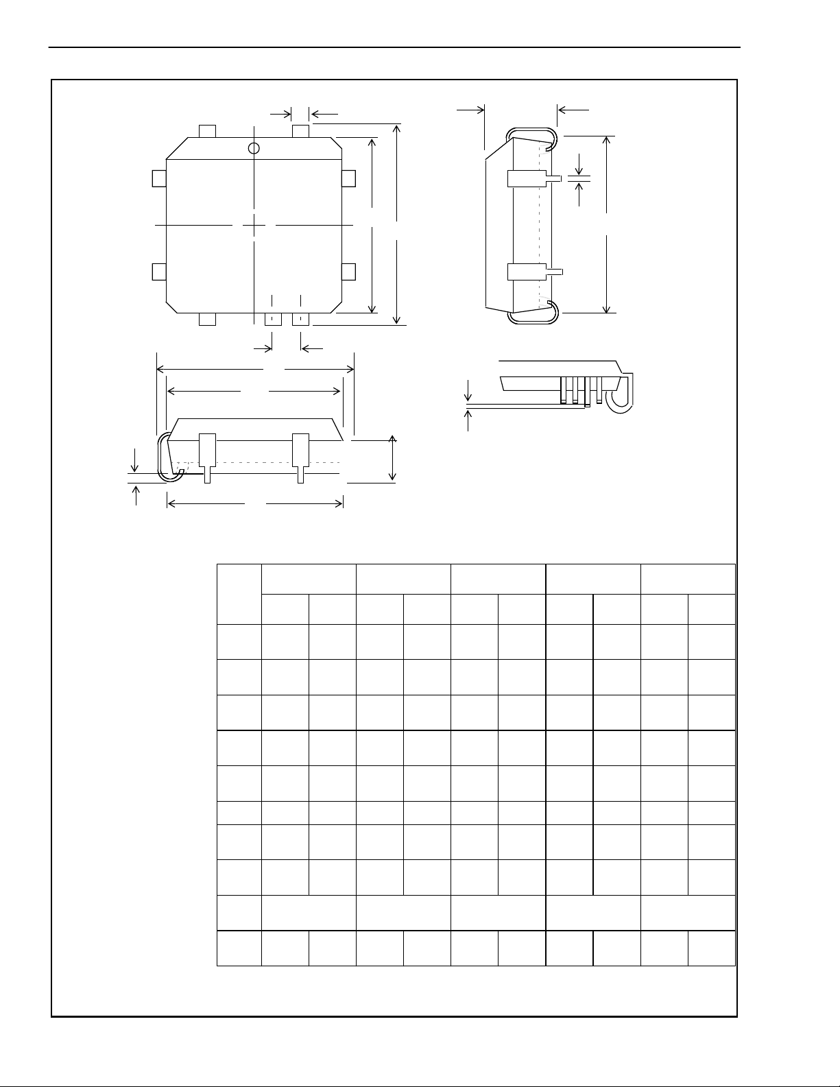
Package Outlines
F
D
1
D
H
E
E
1
e: (lead coplanarity)
A
1
I
E
2
Notes:
1) Not to scale
2) Dimensions in inches
3) (Dimensions in millimeters)
4) For D & E add for allowable Mold Protrusion 0.010"
A
G
D
2
Dim
A
A
D/E
D1/E
D2/E
e
F
G
H
I
20-Pin 28-Pin 44-Pin 68-Pin 84-Pin
Min Max Min Max Min Max Min Max Min Max
0.165
(4.20)
0.090
1
(2.29)
0.385
(9.78)
0.350
1
(8.890)
0.290
2
(7.37)
0.026
(0.661)
0.013
(0.331)
0.020
(0.51)
0.180
(4.57)
0.120
(3.04)
0.395
(10.03)
0.356
(9.042)
0.330
(8.38)
0 0.004 0 0.004 0 0.004 0 0.004 0 0.004
0.032
(0.812)
0.021
(0.533)
0.050 BSC
(1.27 BSC)
0.165
(4.20)
0.090
(2.29)
0.485
(12.32)
0.450
(11.430)
0.390
(9.91)
0.026
(0.661)
0.013
(0.331)
0.050 BSC
(1.27 BSC)
0.020
(0.51)
0.180
(4.57)
0.120
(3.04)
0.495
(12.57)
0.456
(11.582)
0.430
(10.92)
0.032
(0.812)
0.021
(0.533)
0.165
(4.20)
0.090
(2.29)
0.685
(17.40)
0.650
(16.510)
0.590
(14.99)
0.026
(0.661)
0.013
(0.331)
0.050 BSC
(1.27 BSC)
0.020
(0.51)
0.180
(4.57)
0.120
(3.04)
0.695
(17.65)
0.656
(16.662)
0.630
(16.00)
0.032
(0.812)
0.021
(0.533)
0.165
(4.20)
0.090
(2.29)
0.985
(25.02)
0.950
(24.130)
0.890
(22.61)
0.026
(0.661)
0.013
(0.331)
0.050 BSC
(1.27 BSC)
0.020
(0.51)
0.200
(5.08)
0.130
(3.30)
0.995
(25.27)
0.958
(24.333)
0.930
(23.62)
0.032
(0.812)
0.021
(0.533)
(30.10)
(29.210)
(27.69)
(0.661)
(0.331)
0.165
(4.20)
0.090
(2.29)
1.185
1.150
1.090
0.026
0.013
0.050 BSC
(1.27 BSC)
0.020
(0.51)
0.200
(5.08)
0.130
(3.30)
1.195
(30.35)
1.158
(29.413)
1.130
(28.70)
0.032
(0.812)
0.021
(0.533)
General-10
Plastic J-Lead Chip Carrier - P-Suffix
Page 38
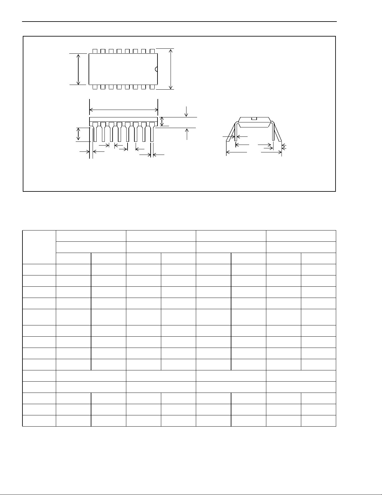
Package Outlines
E
1
D
32
n-2 n-1 n
1
E
L
Notes:
1) Not to scale
2) Dimensions in inches
3) (Dimensions in millimeters)
A
b
D
1
e
2
b
A
2
Plastic Dual-In-Line Packages (PDIP) - E Suffix
8-Pin 16-Pin 18-Pin 20-Pin
DIM
Plastic Plastic Plastic Plastic
Min Max Min Max Min Max Min Max
A
A
2
b
b
2
C
D
D
1
E
E
1
e
e
A
L
e
B
e
C
NOTE: Controlling dimensions in parenthesis ( ) are in millimeters.
0.115 (2.92) 0.195 (4.95) 0.115 (2.92) 0.195 (4.95) 0.115 (2.92) 0.195 (4.95) 0.115 (2.92) 0.195 (4.95)
0.014 (0.356) 0.022 (0.558) 0.014 (0.356) 0.022 (0.558) 0.014 (0.356) 0.022 (0.558) 0.014 (0.356) 0.022 (0.558)
0.045 (1.14) 0.070 (1.77) 0.045 (1.14) 0.070 (1.77) 0.045 (1.14) 0.070 (1.77) 0.045 (1.14) 0.070 (1.77)
0.008
(0.203)
0.355 (9.02) 0.400 (10.16) 0.780 (19.81) 0.800 (20.32) 0.880 (22.35) 0.920 (23.37) 0.980 (24.89) 1.060 (26.9)
0.005 (0.13) 0.005 (0.13) 0.005 (0.13) 0.005 (0.13)
0.300 (7.62) 0.325 (8.26) 0.300 (7.62) 0.325 (8.26) 0.300 (7.62) 0.325 (8.26) 0.300 (7.62) 0.325 (8.26)
0.240 (6.10) 0.280 (7.11) 0.240 (6.10) 0.280 (7.11) 0.240 (6.10) 0.280 (7.11) 0.240 (6.10) 0.280 (7.11)
0.100 BSC (2.54) 0.100 BSC (2.54) 0.100 BSC (2.54) 0.100 BSC (2.54)
0.300 BSC (7.62) 0.300 BSC (7.62) 0.300 BSC (7.62) 0.300 BSC (7.62)
0.115 (2.92) 0.150 (3.81) 0.115 (2.92) 0.150 (3.81) 0.115 (2.92) 0.150 (3.81) 0.115 (2.92) 0.150 (3.81)
0 0.060 (1.52) 0 0.060 (1.52) 0 0.060 (1.52) 0 0.060 (1.52)
0.210 (5.33) 0.210 (5.33) 0.210 (5.33) 0.210 (5.33)
0.014 (0.356) 0.008 (0.203) 0.014(0.356) 0.008 (0.203) 0.014 (0.356) 0.008 (0.203) 0.014 (0.356)
0.430 (10.92) 0.430 (10.92) 0.430 (10.92) 0.430 (10.92)
C
e
A
e
B
e
C
General-8
Page 39
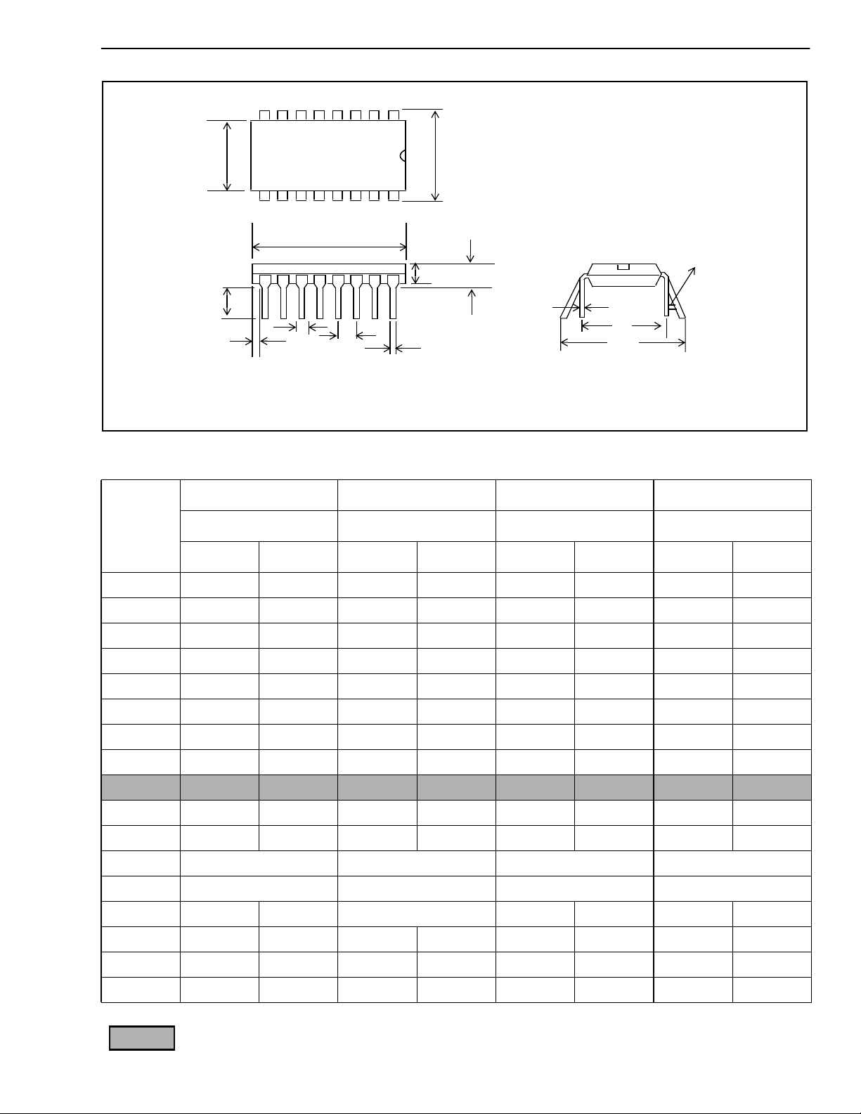
E
1
L
Notes:
1) Not to scale
2) Dimensions in inches
3) (Dimensions in millimeters)
Package Outlines
32
1
E
n-2 n-1 n
D
A
b
D
1
e
2
b
A
2
C
e
A
e
B
Plastic Dual-In-Line Packages (PDIP) - E Suffix
α
DIM
A
A
b
b
2
C
D
D
E
E
E
E
e
e
A
e
A
e
B
L
α
22-Pin 24-Pin 28-Pin 40-Pin
Plastic Plastic Plastic Plastic
Min Max Min Max Min Max Min Max
0.210 (5.33) 0.250 (6.35) 0.250 (6.35) 0.250 (6.35)
2
1
1
1
0.125 (3.18) 0.195 (4.95) 0.125 (3.18) 0.195 (4.95) 0.125 (3.18) 0.195 (4.95) 0.125 (3.18) 0.195 (4.95)
0.014 (0.356) 0.022 (0.558) 0.014 (0.356) 0.022 (0.558) 0.014 (0.356) 0.022 (0.558) 0.014 (0.356) 0.022 (0.558)
0.045 (1.15) 0.070 (1.77) 0.030 (0.77) 0.070 (1.77) 0.030 (0.77) 0.070 (1.77) 0.030 (0.77) 0.070 (1.77)
0.008 (0.204) 0.015 (0.381) 0.008 (0.204) 0.015 (0.381) 0.008 (0.204) 0.015 (0.381) 0.008 (0.204) 0.015 (0.381)
1.050 (26.67) 1.120 (28.44) 1.150 (29.3) 1.290 (32.7) 1.380 (35.1) 1.565 (39.7) 1.980 (50.3) 2.095 (53.2)
0.005 (0.13) 0.005 (0.13) 0.005 (0.13) 0.005 (0.13)
0.390 (9.91) 0.430 (10.92) 0.600 (15.24) 0.670 (17.02) 0.600 (15.24) 0.670 (17.02) 0.600 (15.24) 0.670 (17.02)
0.290 (7.37) .330 (8.38)
0.330 (8.39) 0.380 (9.65) 0.485 (12.32) 0.580 (14.73) 0.485 (12.32) 0.580 (14.73) 0.485 (12.32) 0.580 (14.73)
0.246 (6.25) 0.254 (6.45)
0.100 BSC (2.54) 0.100 BSC (2.54) 0.100 BSC (2.54) 0.100 BSC (2.54)
0.400 BSC (10.16) 0.600 BSC (15.24) 0.600 BSC (15.24) 0.600 BSC (15.24)
0.300 BSC (7.62)
0.430 (10.92)
0.115 (2.93) 0.160 (4.06) 0.115 (2.93) 0.200 (5.08) 0.115 (2.93) 0.200 (5.08) 0.115 (2.93) 0.200 (5.08)
15° 15° 15° 15°
Shaded areas for 300 Mil Body Width 24 PDIP only
Page 40

http://www.mitelsemi.com
World Headquarters - Canada
Tel: +1 (613) 592 2122
Fax: +1 (613) 592 6909
North America Asia/Pacific Europe, Middle East,
Tel: +1 (770) 486 0194 Tel: +65 333 6193 and Africa (EMEA)
Fax: +1 (770) 631 8213 Fax: +65 333 6192 Tel: +44 (0) 1793 518528
Fax: +44 (0) 1793 518581
Information relating to products and services furnished herein by Mitel Corporation or its subsidiaries (collectively “Mitel”) is believed to be reliable. However, Mitel assumes no
liability for errors that may appear in this publication, or for liability otherwise arising from the application or use of any such information, product or service or for any infringement of
patents or other intellectual property rights owned by third parties which may result from such application or use. Neither the supply of such information or purchase of product or
service conveys any license, either express or implied, under patents or other intellectual property rights owned by Mitel or licensed from third parties by Mitel, whatsoever.
Purchasers of products are also hereby notified that the use of product in certain ways or in combination with Mitel, or non-Mitel furnished goods or services may infringe patents or
other intellectual property rights owned by Mitel.
This publication is issued to provide information only and (unless agreed by Mitel in writing) may not be used, applied or reproduced for any purpose nor form part of any order or
contract nor to be regarded as a representation relating to the products or services concerned. The products, their specifications, services and other information appearing in this
publication are subject to change by Mitel without notice. No warranty or guarantee express or implied is made regarding the capability, performance or suitability of any product or
service. Information concerning possible methods of use is provided as a guide only and does not constitute any guarantee that such methods of use will be satisfactory in a specific
piece of equipment. It is the user’s responsibility to fully determine the performance and suitability of any equipment using such information and to ensure that any publication or
data used is up to date and has not been superseded. Manufacturing does not necessarily include testing of all functions or parameters. These products are not suitable for use in
any medical products whose failure to perform may result in significant injury or death to the user. All products and materials are sold and services provided subject to Mitel’s
conditions of sale which are available on request.
M Mitel (design) and ST-BUS are registered trademarks of MITEL Corporation
Mitel Semiconductor is an ISO 9001 Registered Company
Copyright 1999 MITEL Corporation
All Rights Reserved
Printed in CANADA
TECHNICAL DOCUMENTATION - NOT FOR RESALE
 Loading...