

Page 1
ISO-CMOS ST-BUS FAMILY
MT8926
T1 Performance Monitoring
Adjunct Circuit (PMAC)
Features
• ANSI T1.403 and T1 .408 Perfo rmance
Monitoring and Main t ena nc e Functions
• Operates in c onjun ction wi th Mitel 's T1/ES F
framer circu its (M T897 6/77 and MH 89760 B)
• D3/D4 (SF), and ESF modes of operation
• One and two second timers
• Supports bit-oriented and message-oriented
data transfe r over the F acility D ata Link (FDL )
• ESF and D3/D4 Yellow Alarms, Alarm Indication
Signal an d Loss of Sig nal Indi cati on
• Framing Error, CRC Error and Bipolar Violation
Error counters
• Alarm interrup t s and counter overfl ow i nt er r up ts
Applications
• T1 line perfor mance data collect ion
• CSU performa nce monitori ng
• ISDN Primary Rate maintenance controller
ISSUE 3 July 1993
Ordering Information
MT8926A E 28 Pin Plast ic DIP
MT8926A P 28 Pin PLC C
-40°C to 85°C
Description
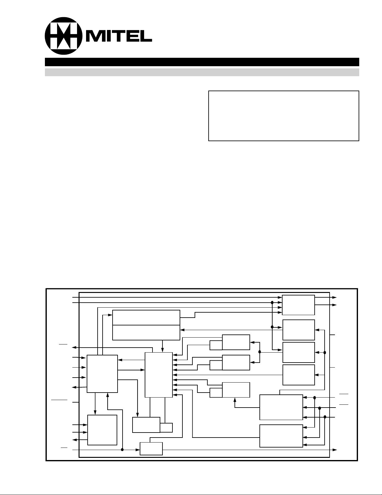
The MT8926 Performance Monitoring Adjunct Circuit
(PMAC) interworks with Mitel's MT8976/77 and
MH89760B to provide performance monitoring data,
alarms and T1 maintenance features.
It meets the performance monitoring and
maintenance requirements of ANSI T1.403 and
T1.408, and also supports Channel Service Unit
(CSU) requirements.
FDLi
E8Ki
IRQ
C2i
CSTi0
CSTi1
CSTo
RESET
DSTi0
DSTi1
DSTo
F0i
ST-BUS
Interface
Payload
& Li ne
Loopback
Control
Transmit BOM
Register
Receive BOM Registe r &
RAI Debounce
Snap -
Shot
Registers
8 Bit CRC
Counter
CSI
Timer
Figure 1 - Functional Block Diagram
SEI
FSI
BSI
4 Bit SE
Counter
4 Bit FE
Counter
8 Bit BPV
Counter
E8K/FDL
Extractor
Framer,
Detector
Loopback
Integrator
B8ZS
Recovery,
BPV Detector
AIS/LOS
Detector
Mux
FDL
SE/FE
Line
E8Ko
FDLo
V
DD
V
SS
RxA
RxB
ECLK
1SEC
4-3
Page 2
MT8926
VSS
ECLK
RxA
RxB
E8Ki
E8Ko
VSS
CSTo
CSTi0
CSTi1
VSS
1
2
3
4
5
IC
6
7
8
9
10
11
12
F0i
C2i
13
14
28 PIN PLASTIC DIP
28
27
26
25
24
23
22
21
20
19
18
17
16
15
VDD
IC
DSTi1
DSTi0
DSTo
IC
VSS
IC
IRQ
1SEC
FDLo
FLDi
RESET
VDD
IC
E8Ki
E8Ko
VSS
CSTo
CSTi0
CSTi1
RxB
432
5
6
7
8
9
10
11
12 13 14 15 16 17 18
28 PIN PLASTIC J-LEAD
1
F0i
C2i
VSS
VDD
VDD
RESET
DSTi1
IC
262728
25
24
23
22
21
20
19
FLDi
FLDo
VSS
ECLK
RxA
DSTi0
DSTo
IC
VSS
IC
IRQ
1SEC
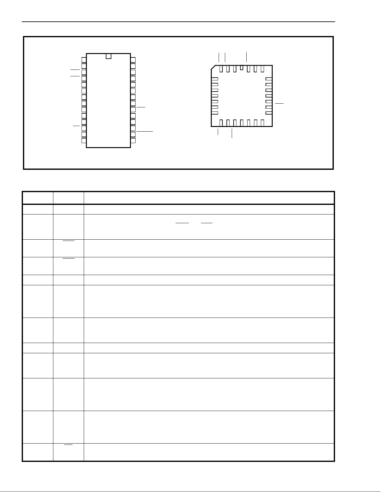
Figure 2 - Pin Connections
Pin Description
Pin # Name Descrip tio n
1V
2ECLKExtracted Clock Input. A 1.544 MHz clock derived from the received data. This signal is
3RxA
4RxB
5ICInternal Connection. Must be tied to V
6E8KiExtracted 8 kHz Input. A low going pulse on this input is used by the PMAC to locate the
7E8Ko8 kHz clock output. The 8 kHz signal input at E8Ki is output on this pin when bit 2 (8KEn)
8V
9 CSTo Con trol ST-BUS Output. The data that enters the PMAC on CSTi0 will exit th e device on
10 CSTi0 Control ST-BUS Input 0. Accepts the serial ST-BUS stream output on CSTo of the
11 CSTi1 Control ST-BUS Input 1. Channel 11 of this ST-BUS input stream is used to control
12 F0i
System Ground.
SS
used to clock in the data on pins RxA
and RxB.
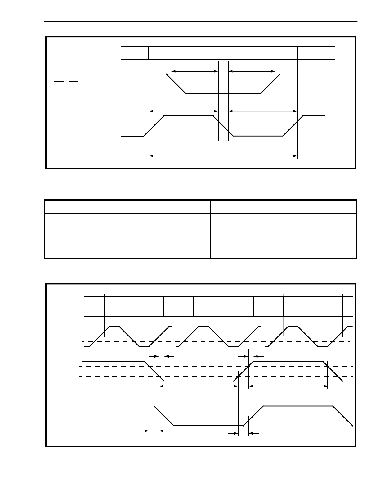
See Figure 11 for timing informati o n.
Receive A Input. A unipolar active low signal deco ded from the received T1 signal. See
Figure 11 for timing information.
Receive B Input. A unipolar active low signal decoded from the rece ived T1 signal. See
Figure 11 for timing information.
for normal operation.
SS
framing bit in the received signal. The device use s this inform ation t o detect errors in the
received framing bits. Connect to E8Ko of the MT8976/ 77. See Figure 12 for timing
information.
of the PMAC Control Word is set. The output is pulled high when 8KE n is reset. See
Figure 12 for timing informat ion.
System Ground.
SS
this pin. Data derived by the PMAC will be inserted into specific channels of this output
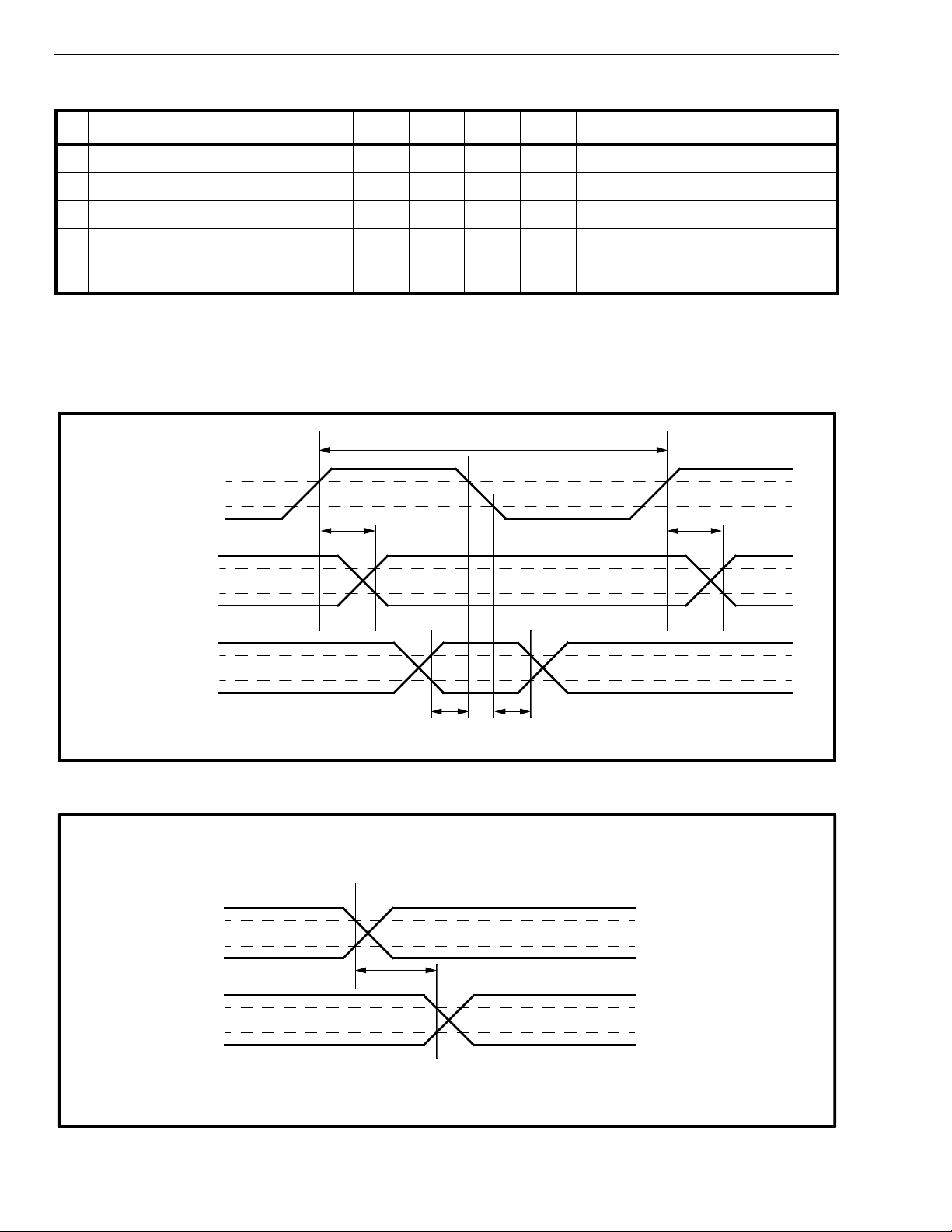
stream. See Figures 13 and 14 for timing informati on and Figu re 5 for channel allocation.
MT8976/77. The data tha t ente rs the PMAC on this pin exit s the device on CSTo. The
contents of specific CSTi0 channels is replaced by data derived by the PMAC. See Figures
13 and 14 for timing information and Figure 4 for channel allocat ion .
specific features in the device (Table 14). Channel 7 is used for the transmit bit-oriented
message (Table 13), and channel 15 is used to control loopback functions (Table 4). See
Figure 13 for timing information and Fig ure 3 for channel allocation.
Frame Pulse Input. This input accepts an 8 kHz signal, which is used to delineate the S TBUS frame boundary. See Figure 15 for timing information.
4-4
Page 3

MT8926
Pin Description (Con t inued)
Pin # Name Descrip tio n
13 C2i 2.048 MHz Clock I nput. This input accepts a 2.048 MHz clock signal, which is used to
clock ST-BUS control and data streams into and out of the PMAC. See Figures 13 and
14 for tim i ng in fo rmation.
14 V
15 V
16 RESET
17 FDLi Facility Data Link Input. This input accepts a 4 kbit/sec. facility data link transmit
18 FDLo Facility Data Link Output. When bit-oriented messaging is enabled (i.e., PMAC
19 1SEC 1 Second Output. A one second timing signal derived from the ST-BUS F0i
System Ground.
SS
Supply Voltage Input (+5 V).
DD
RESET Input. Must be high for normal operation. When low, the functions of the
MT8926 will be suspended.
signal, which is routed back out transparently on FDLo if message-oriented signal
transmis sion is enabl ed (i.e., PMAC Co ntrol Word bit 0, FDL En, is low). This s ignal is
not clocked into the PMAC. If bit-oriented messaging is enabled (FDLEn high), data on
this input will not be routed to FDLo (see pin 18, FDLo, below).
Control Word bit 0, FDLEn, is high), data in the Transmit BOM register will be appended
to a 1111 1111 (FF) flag and clocked out of the device at this output. The output timing
for this s ignal is shown in Figure 18. When bit-oriented messaging is disabled (FDLEn
low), data received at the FDLi pin is routed back out transparently on this pin (it is not
re-timed). See Figure 19 for timing information.
output on this pin. The output is low for 0.5 seconds and high for 0.5 seconds. It can be
used as an interrupt source to generate T1.403 message-oriented performance reports.
See Figure 16 for t iming information.
signal is
20 IRQ
Interrupt Request Ou tput. An open drain output that is to be externally connected to
through a pull-up resistor. The PMAC will pull this pin low to assert an interrupt
V
DD
request. Interrupting events and their groupings are described in Tables 16 and 17. IRQ
is released by making bit 1 (Interrupt Acknowledge - INTA) of the PMAC Control Word
low. Once INTA is set, all interrupting signals of a particular group must be inactive
before the next interrupt of that group can assert IRQ
. See Figure 17 for functional
timing information.
21 IC Internal Connection. Must be left open for normal operation.
22 V
System Ground.
SS
23 IC Internal Connection. Must be left open for normal operation.
24 DSTo Data ST-BUS Output. A 2.048 MBit/sec. serial output stream, which contains the 24
PCM or data channels to be transmitted on the T1 trunk. This data stream is
multiplexed from either input DSTi0 (Normal Mode) or input DSTi1 (Payload Loopback
Mode). The selection of either the Normal or Payload Loopback mode is made through
the Loopback Control Word. This output should be connected to DSTi of the MT8976/
77. When the loopback control word is set for line loopback code generation, the 24
PCM channels will contain the line loopback activate or deactivate code stream. See
Figure 14 fo r ti mi n g information.
25 DSTi0 Data ST-BUS Input 0. A 2.048 MBit/sec. serial input stream, which contains the 24
PCM or data channels to be transmitted on the T1 trunk in Normal Mode. This input
should be connected to the system side output stream.
26 DSTi1 Data ST-BUS Input 1. A 2.048 MBit/sec. serial input stream, which contains the 24
PCM or data channels to be transmitted on the T1 trunk in Payload Loopback Mode.
This input should be connected to DSTo of the MT8976/77.
27 IC Internal Connection. M u st be tied to V
28 V
Supply Voltage Input (+5 V).
DD
for normal operation.
SS
4-5
Page 4
MT8926
Functional Description
The MT8926 Performance Monitoring Adjunct Circuit
(PMAC) is designed to enable a MT8976/77 based
T1 interface to gather performance data and perform
maintenance functions as per ANSI T1.403 and
T1.408. Performance data collection includes CRC
errors, severely errored framing events, frame
synchronization-bit errors, line code violations, and
controlled slips. Maintenance functions include the
detection of alarms, SF line loopback code
generation and detection, ESF payload loopback, as
well as the transport of bit-oriented and messageoriented signals over the Facility Data Link (FDL).
The control and status data of the MT8926 is
transported over spare channels of the existing
MT8976/77 ST-BUS streams. Therefore, no new STBUS streams are required to upgrade with the
PMAC.
The PMAC has an on-board framer that uses the
received signal and extracted 8 kHz clock to achieve
synchronization. The result of this frame alignment is
logically ANDed with the SYN bit of the MT8976/77
CSTo stream to give FECV (see Table 5). This will
ensure that the PMAC can only declare
synchronization after the framer is synchronized.
The MT8926 will align to SF or ESF framing without
user selection.
An interrupt (IRQ output) system is also provided to
reduce the requirement to monitor ST-BUS channels
continuously for exception conditions. Interrupt
sources are divided into group one (G1) for service
affecting events and group two (G2) for counter
overflows.
A timer has been included to allow scheduling of
T1.403/408 message-oriented performance reports
for transmission over the facility data link. This timer
provides a two second output (register accessed)
and a one second output pin.
Two eight bit counters with overflow bits and resets
(resets counter and overflow bit) are provided to
record line code violations (BPV) and CRC errors.
The BPV counter will not count B8ZS encoding
violations. When either overflow bit goes high it will
generate a group two (G2) interrupt.
Two four bit counters are used to record framing
error events (FE) and severely errored framing
events (SE). The FE counter has an overflow
indication bit and can be cleared (resets counter and
overflow bit) by the user. Its overflow bit will generate
a group two (G2) interrupt when it goes high. A G2
interrupt will also be issued whenever the SE co unter
is incremented.
The alarms that the PMAC monitors are alternate SF
yellow ala rm (i.e., twelfth SF fr aming bit =1, ALR M),
ESF facility data link yellow alarm (RAI), loss of
signal (i.e., reception of 128 or more consecutive
zeros), and alarm indication signal (AIS, blue alarm
or all ones alarm). Theref ore, the MT8926/MT8976/
77 combination supports a comprehensive alarm
package.
The PMAC alarm registers and counters are updated
as the corresponding events occur. Once per frame
(8000 times a second) the state of these registers
and counters is recorded in a set of snap-shot
registers. This data in the snap-shot registers is then
inserted into the appropriate bit positions of the STBUS status stream CSTo.
FDL bit-oriented messages can be communicated
via the PMAC transmit and receive bit-oriented
message registers. The user gains access to these
register s th rough the S T-BUS co ntro l stre ams. Valid
bit-oriented messages consist of a series of
0-2
3X4-6
CSTi1
T1 1-3 4-6 7-9 10-12 13-15 16-18 19-21 22-24
PCCW = Per Channel Control Word
PCCW
2
Bit
PCCW
Transmit Bit-Oriented
Message Register
7
0
Function
Transmitted First
Transmitted Last
7
8-10
Tx
PCCW
2
BOM
11
12-14
PC
PCCW
2
W
PMAC Control Word
Bit
7
6
5
4
3
2
1
0
2
Function
SER
FER
CRCR
BPVR
FSel
8KEn
INTA
FDLEn
15
LC
W
16-18
PCCW
2
Bit 1
0
0
1
1
19X20-22
PCCW
2
Loopback Control
Word
Bit 0
0
1
0
1
Normal
Payload Loopback
Line Loopback Enable Code (00001)
Line Loopback Disable Code (001)
23X24-26
PCCW
Function
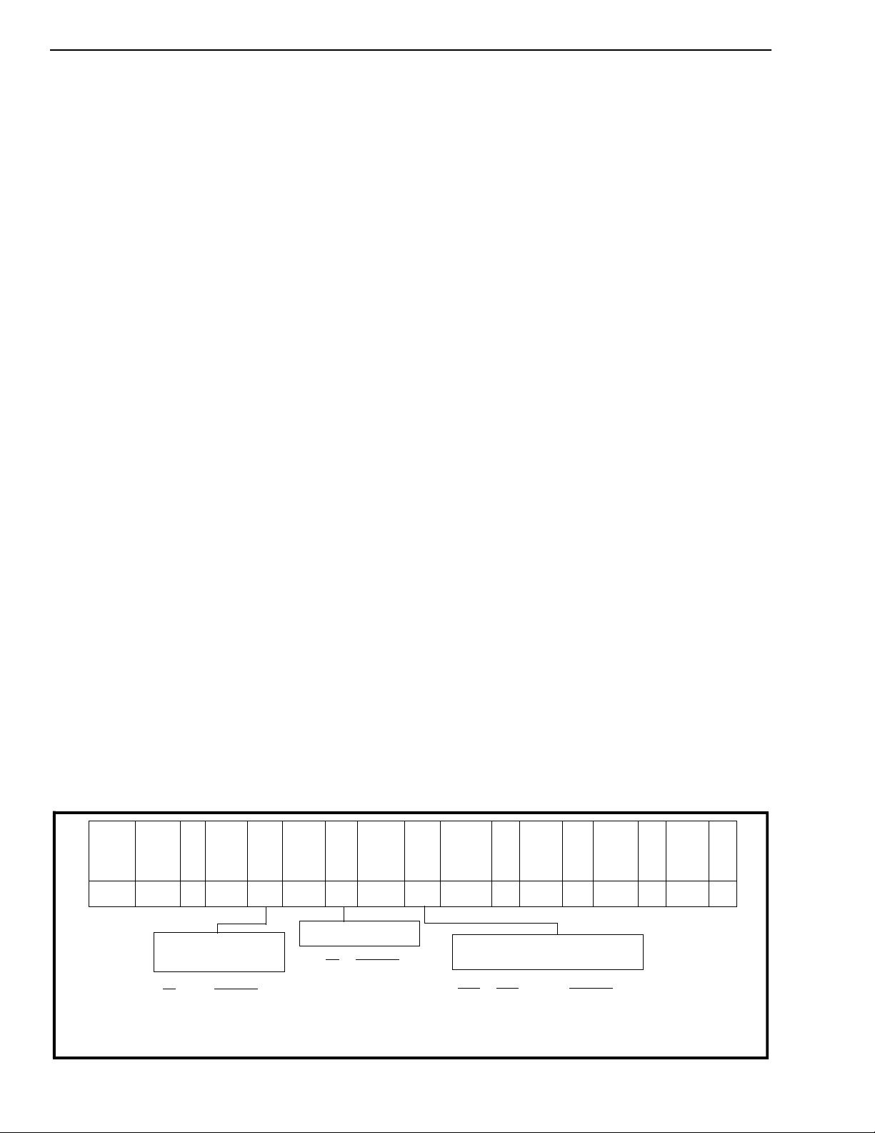
FIgure 3 - C STi1 Ch anne l A llo cat ion Versus T1 C han ne ls
4-6
2
27X28-30
PCCW
2
31
X
Page 5
MT8926
repeating 16 bit code words of the form: 11111111
0XXXXXX0, where X XXXXX is the message content.
The PMAC will automatically append the prefix byte
11111111 to the transmit message and remove it fro m
the receive message. It will also indicate the
reception of a valid message. When bit-oriented
messages are not being transported, messageoriented facility data link signals, assembled by an
external HDLC controller (i.e., MT8952), can be
passed through the PMAC to the MT8976/77 for
transmission.
The PMAC can implement an ESF payload loopback
by routing the MT8976/77 DSTo stream to the
MT8976/77 DSTi input (see Figure 6). The payload
loopback is controlled through the loopback control
word, Channel 15 of CSTi1 (see Figure 3). When the
payload loopback is disabled, data entering the
PMAC’s DSTi0 pin is transferred to the PMAC DSTo.
DSTo of the PMAC should be connected to the DSTi
pin of the MT8976/77 framer.
PMAC - Framer Interw orking
The MT8926 PMAC is designed to function with the
MT8976/77 T1 framer. Figure 9 illustrates a typical
application and the connections involved in realizing
this interface . Bo th th e P MAC a nd framer receive th e
extracted clock and data from the T1 line interface.
This allows the MT8926 to perform B8ZS recovery
and BPV detection, as well as SF or ESF
synchronization, framing error det ection, facility data
link extraction, and line loopback code detection.
Some of the CSTi1 channels that are not used to
control the MT8976/77 are used to control the
PMAC, therefore, CSTi1 will connect to both devices.
Figure 3 shows the channels of CSTi1 that carry the
MT8976/77 Per Channel Control Words, as well as
the MT8926 control dat a. C2i and F0i
supply timing
references for both d e vices.
The CSTo stream of the MT8976/77 framer enters
the PMAC on CSTi0 (see Figure 4). The PMAC adds
its performance data to form the CSTo stream of the
PMAC. Figure 5 shows the channels and status bits
that the PMAC has added to CSTo. E8Ko of the
framer will also pass through the PMAC, E8Ki to
E8Ko, under control of CSTi1.
It should be noted that the PMAC will replace some
of the data of MT8976/77 Master Status Words 1 and
2. This is outlined in Tables 1 and 2.
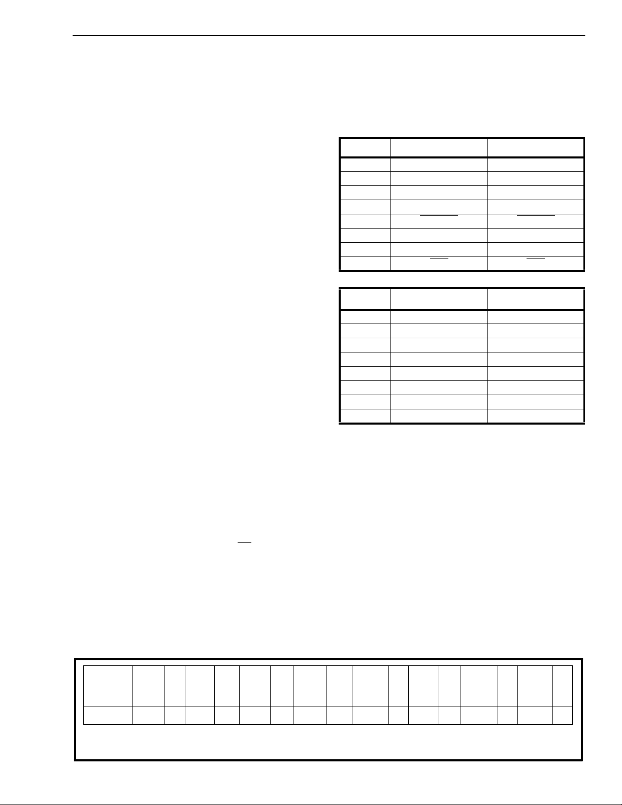
Bit MT8976/77 CSTo MT8926 CSTo
7 YLALR YLALR
6 MIMIC MIMIC
5 ERR ALRM
4 ESFYLW RAI
3 MFSYNC
2 B PV LOS
1 SLIP SLIP
0SYN
MFSYNC
SYN
Table1. Maste r Status Word 1 Data Su bstitu tion
Bit
7 BlAlm BlAlm
6FrCnt FrCnt
5 Xst Xst
4 BPVCnt SEI
3 BPVCnt FSI
2 CRCCNT CSI
1 CRCCNT BSI
0 CRCCNT AIS
MT8976/77 CSTo MT8926 CSTo
Table 2. Master Stat us Wo rd 2 Data Su b stitution
The MT8926 can be programmed to either pass data
through from FDLi to FDLo and on to the MT8976/77
input TxFDL, or insert bit-oriented messages into the
FDL via the transmit bit-oriented message register,
channel 7 of CSTi1. This function is under control of
the FDLEn bit of the PMAC Control Word. See
Application section Figure 9 for FDL connections.
Channel 15 of CSTi1, the Loopback Control Word, is
used to control the line loopback code generation
and payload loopback functions of the PMAC. This is
done by internally connecting the MT8926 DSTo to
either a line loopback enable code generator, a line
loopback disable code generator, DSTi0 or DSTi1.
Figure 6 illustrates the connections required to
support these functions. The DSTo of the framer
CSTi0
MT8976/77
CSTo
T1 1-3 4-6 7-9 10-12 13-15 16-18 19-21 22-24
PCSW
PSW
MSW
0-2
PCSW3PS
=
Per Channel Status Word
=
Phase Status Word
=
Master Status Word
PCSW7X
W
4-6
8-10
PCSW11X
12-14
PCSW15MS
W1
16-18
PCWS19X
20-22
PCSW23X
24-26
PCSW27X
24-26
PCSW31MS
FIgure 4 - MT 8926 CSTi0 (M T897 6/77 C STo) Channel Alloc atio n Versus T1 Chan nels
W2
4-7
Page 6
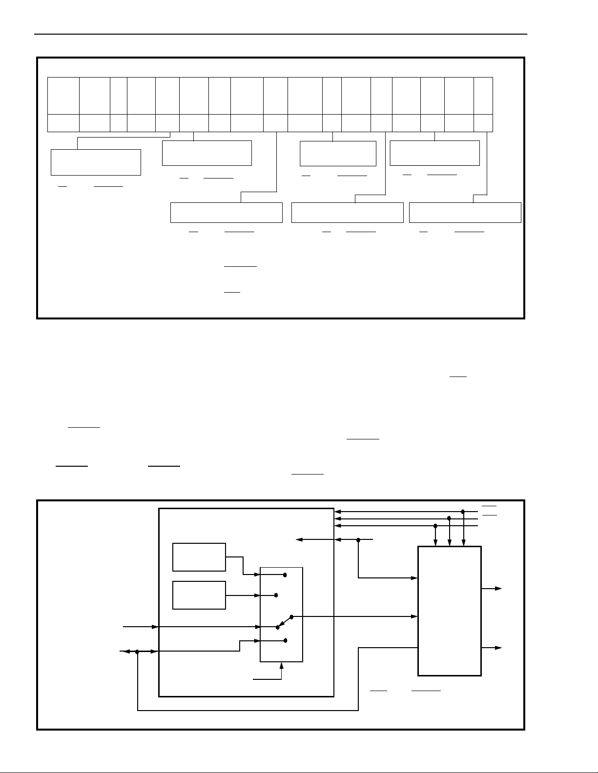
MT8926
0-2
3
4-6
CSTo
T1 1-3 4-6 7-9 10-12 13-15 16-18 19-21 22-24
PCSW
PS
PCSW7PM
W
SW
8-10
PCSW11CRC
12-14
PCSW15MS
W1
16-18
PCSW19EF
EC
20-22
PCSW23BPV
24-26
PCSW
2
27
Rx
BOM
28-30
PCSW31MS
W2
Cyclic Redundancy
PMAC Miscellaneous
Status Word
Bit
7-5
4
3
2
1
0
PCSW = Per Channel Status Word
PSW = Phase Status Word
* MT8976/77 Data unaltered by
the MT8926
Function
Not Used
LLDD (001)
LLED (00001)
FECV
TMR (2SEC)
BOMV
Check-6 Error Counter
Bit
Function
7MSB
0
LSB
Master Sta tus Word 1
Bit
7*
6*
5
4
3*
2
1*
0*
Function
YLALR
MIMIC
ALRM
RAI (ESF YELLOW)
MFSYNC
LOS
SLIP
SYN
Figur e 5 - CSTo Chan ne l All oca t ion Versus T1 C han ne ls
connects to DSTi1 of the PMAC and to the receive
side of the system. This allows the PMAC to perform
a payload loopback by internally connecting DSTi1 to
DSTo. In normal operation, transmit data will flow
from DSTi0 to DSTo of the PMAC to DSTi of the
MT8976/77.
Errored Frame
Event Counter
Bit
7-4
3-0
Function
SE (MSB-LSB)
FE (MSB-LSB)
Bipolar Violation Counter Master Status Word 2
Function
Bit
7MSB
0
LSB
Received Bit-Oriented
Message Register
Bit
Function
7
Received First
0 Received Last
Bit
7*
6*
5*
4
3
2
1
0
Function
BlAlm
FrCnt
Xst
SEI
FSI
CSI
BSI
AIS
normal operation). In the reset state, data entering
the PMAC on FDLi, DSTi0 and CSTi0 will pass
through unaltered to FDLo, DSTo and CSTo
respectively. E8Ko will be high, IRQ
will be high
impedance and the 1SEC output (and TMR bit) will
be low.
PMAC RESET
The MT8926 functions may be suspended by making
the RESET
input low (RESET must be high for
MT8926
To PMAC
Control
4 to 1 MUX
LCW
ST-BUS Transmi t
Data Stream
ST-BUS Receive
Data Stream
LCW = Loopback Control Word
Repeating
Repeating
DSTi0
DSTi1
001
00001
Figure 6 - Payload and Line Loopback Operation
After the MT8976/77 has acquired frame synchronization and RESET
returns high, the MT8926 will
require two superframes to acquire synchronization
and two ST-BUS frames to align to the ST-BUS.
RESET
can be used to prevent DS1 interface
RxA
RxB
CSTi1
DSTo
From System
Control
LCW
0 0
0 1
1 0
1 1
DSTi0 to DSTo
DSTi1 to DSTo
00001 to DSTo (activate )
001 to DSTo (deactivate)
MT8976/77
CSTi1
DSTi
DSTo
Function
ECLK
TxA
TxB
4-8
Page 7

Bit Name Description
MT8926
7-6 YLALR
&
MIMIC
5 A LRM Alarm . This bit will be set if the MT8926 detect s a 1 in the F
These bits (Yellow Alarm Indication and Mi mi c) contain informa tio n from the
MT8976/77 that is unalte red by the MT8 926. See Master Stat us Word 1 of the
MT8976/77 data sheet.
bit position of the
S
twelfth frame of an SF superframe (alternate yellow alarm indication). ALRM will be
low when the F
bit is 0.
S
When receiving an ESF signal or if bit 3 (FSEL) of the PMAC Control Word (CSTi1
Channel 11) is low, the ALRM bit will always be low.
4 RAI Rem ot e Alarm In dicat ion (also kn own as ESF Yellow Alarm). This bit is set if an
RAI code word (repeating hex FF00 pattern) is received on the ESF facilit y data
link. This code must be correctly detected in seven out of 10 messages. RAI will be
reset if more than three of 10 messages are in error.
When receiving an SF signal, this bit will always be low.
3MFSYNC
This bit (Multiframe Synchronization) contains information from the MT8976 that is
unaltered by the MT8926. See Master S tatus Word 1 of the MT8976 data sheet.
2 LOS Loss of Signal. This bit will go high when the MT8926 detects 128 or more
consecutive zeros in the line signal. It will be reset after the device detects a 12.5%
ones density (48 ones in two or less frames) in the received signal.
1-0 SLIP
&
SYN
These bits (Slip Ind ication and Synchron izati on) contain inform at ion from the
MT8976/77 that is unalte red by the MT8 926. See Master Stat us Word 1 of the
MT8976/77 data sheet.
Table 3. M aster S tat us Word 1 (CSTo Channe l 15)
Bit 1 Bit 0 Description
0 0 Normal operation. The transmit data applied to DSTi0 will pass through the PMAC, and be
output on DSTo.
0 1 Payload Loopback mode. Connect as per Figure 6. The received data on DSTo of the
MT8976/77 is routed through th e PMAC to the DSTi input of the MT8976/77.
1 0 Transmit Line Loopback Enable. Connect as per Figure 6. DSTo of the PMAC will be internally
connected to an SF line loopback enable code generat or. That is, a repeating 00001 code is
placed in the 24 T1 channels of DSTo, so it may be transmitted by the framer.
1 1 T ransmit Line Loopback Disable. Connect as per Figure 6. DSTo of the PMAC will be internally
connected to an SF line loopback disable code generator. That is, a repeating 001 code is
placed in the 24 T1 channels of DSTo, so it may be transmitted by the framer.
Table 4 - Loopback Control Word (CSTi1 Cha nne l 15)
Note: Bits 2 to 7 of the Loopback Control Word are not used.
interrupts from occurring during system
initialization. It should be noted that when the
an ESF signal is being received or when FSel is low,
ALRM will always be low.
MT8926 is acquiring synchronization the CRC and
BPV counters may record errors.
A low to high transi tion of the ALR M bit will in itiate a
group one (G1) interrupt.
ALRM (SF Yellow Alarm)
Remote Alarm Indica tion (RAI)
The MT8926 will recognize the sixth F
superframe as an alternate Yellow Alarm indicator, if
FSel of the PMAC Control Word is high. That is,
when this F
bit is high/low, the ALRM bit of Master
S
Status Word 1 will be high/low (see Table 3). When
bit of an SF
S
The PMAC will decode the bit-oriented priority
codeword 11111111 0000 0000 received on the FDL
as a Remote Alarm Indication (RAI or Yellow Alarm)
signal as per T1.403/408. See the section on
4-9
Page 8

MT8926
MT8926 FDL message transfer. This 16 bit pattern
must be detected in seven out of 10 codewords in
(approximately 48 ones is received in two or less
frames).
order for the RAI bit of Master Status Word 1 (CSTo
channel 15 bit 4) to go high (see Table 3). If more
than three out of 10 codewords are in error, then RAI
Payload Loopback
will remain low.
The payload of a T1 signal consists of the 192 data
A low to high transition of the RAI bit will initiate a
group one (G1) interrupt. See the section on
interrupts fo r t he control of th e R AI interrupt.
bits of each frame and excludes the framing bit (the
first bit of 193). Therefore, a T1.403 or T1.408 ESF
payload loopback extracts the payload of a receive
T1 signal and transmits it back to the originator with
new framing bits. This allows the transport of
Loss of Signal Indication (LOS)
maintenance and performance data over the facilit y
data link while the payload loopback is activated.
The LOS bit of M aster Status Word 1, Table 3, will be
high if the MT8926 receives 128 or more consecutive
zeros from the T1 interface. LOS will return low when
The CRC-6 multiframe alignment remainder will not
be looped around, but will function normally (i.e.,
calculated for each direction of transmission).
a ones density of 12.5% has been achieved
Bit Name Description
7-5 --- Not Used.
4 LLDD Line Loopback Disable Detect. This bit is set when a repeating 001 pattern (either
framed or unframed) is detected in the received T1 signal for at least five frames.
In order to comply with T1.403, the user's operating system will ensure that this
code is present for at least five seconds before deactivating the S F line loopback
(MT8976/77 Remote Loopback).
)
The MT8926 will detect this repeating bit pattern even in the presence of a BER of
3 errors in 1000 bits.
3 LLED Lin e Loopback Ena ble Det e ct. This bit is set when a repeating 00001 pattern
(either framed or unfram ed) is detect ed in the received T1 signal for at least five
frames. In order to comply with T1.403, the user's operating system will ensure
that this code is present for at least five seconds before activating the SF line
loopback (MT8976/77 Remote Loopback).
The MT8926 will detect this repeating bit pattern even in the presence of a BER of
3 errors in 1000 bits.
2 FECV Framing Error Count Validation. This bit is set when the MT8926 has synchronized
to a framed T1 signal. The framing error count is frozen if this bit is not set.
Synchronization (FECV =1) is reported when the MT8926 det ects two consecuti ve
superframes with correct framing bits, and bit 0 in CSTi0 channel 15 (SYN
When receiving an SF signal, both F
the PMAC Control word is set. In this case the sixth F
checking for framing bits. If bit FSel is reset, then only F
and FT bits are examined if bit 3 (FSel) in
S
bit is not examined when
S
bits are examined.
T
Loss of synchronization (FECV=0) is reported when either two out of four errors
have been detected in the received framing bit position (S F F
bits) or if bit 0 in CSTi0 channel 15 (SYN
) is set indicating the MT8976/77 has lost
bits or ESF FPS
T
synchronization.
1 TMR Two Second Timer. This bit changes state once per second.
0 BOM V Bit-Oriented Messa g e Validation. This bit will be set when a valid bit-oriented
message is present in the receive BOM register (T able 12, CSTo, channel 27). It is
reset when a valid message is not being received. A valid bit-oriented message
has the form 111111110XXXXXX0, where XXXXXX co ntains the messag e
information.
Table 5. PMAC Miscell ane ous Sta tus Word (C STo Channel 7)
4-10
) is zero.
Page 9

MT8926
The MT8926 PMAC can perform a payload loopback
by muxing the data received on the MT8976/77’s
DSTo to DSTi of the MT8976/77. This is controlled by
the MT8926 Loopback Control Word (CSTi1 channel
15, see Table 4).
Figure 6 illustrates the MT8926 payload loopback
connections. The ST-BUS transmit stream (normally
connected to DSTi of the MT8976/77) will connect to
DSTi0 of the MT8926. The DSTo stream of the
MT8976/77 will connect to DSTi1 of the MT8926 and
to the ST-BUS receive stream. DSTo of the MT8926
will connect to DSTi of the MT8976/77.
Line Loopback Codes
T1.403 defines SF mode line loopback activate and
deactivate codes. These codes are either a framed
or un-framed repeating bit sequence of 00001 for
activation or 001 for deactivation. The standard goes
on to say that these codes will persist for five
seconds or more before the loopback action is taken.
The MT8926 will generate line loopback activate and
de-activate codes. These functions are controlled by
the Loopback Control Word of CSTi1 channel 15
(see Table 4). The connections illustrated in Figure 6
must be implemented for this feature to function.
The MT8926 will also detect both framed and unframed line loopback activa te and de-activate codes
even in the presence of a BER of 3 errors in 1000
bits. See the PMAC Miscellaneous Status Word,
Table 5, CSTo channel 7 bit 3 Line Loopback Enable
Detect (LLED) and bit 4 Line Loopback Disable
Detect (LLDD). The line loopback of T1.403 is
equivalent to the remote loopback function of the
MT8976/77 (see MT8976/77 data sheet, Master
Control Word 2). Therefore, the user will monitor the
LLED and LLDD bits to ensure that they persist for a
minimum of five seconds. Then the line loopback can
be either activated or de-activated using the
MT8976/77 Remote Loopback function.
PMAC Synchronization
The MT8926 has its own frame synchronization
mechanism, which uses the received signal (RxA
and RxB) and E8Ki to achieve SF and ESF frame
and superframe alignment. Further, the PMAC
monitors the SYN
bit of the MT8976/77 (CSTo
channel 15 bit 0) and will not declare synchronization
until it is clear. When SYN
is low and the MT8926
framer is properly aligned for two superframes, the
PMAC will declare synchronization by making the
Frame Error Count Validation bit (FECV) high. If this
criteria is not met, FECV will be low.
The PMAC will use the received F
and FS bits, F
T
bits only or FPS bits to acquire synchronization. The
receive F
or FPS bit s are used to determine the out-
T
of-synchronization state (see Table 5).
Tim er O ut put s
The PMAC has two timer outputs, 1SEC pin and
CSTo TMR bit, which are derived from the 8 kHz STBUS frame pulse F0i
. These signals have been
implemented to provide the interface controller with a
timing reference for the transmission of T1.403/408
message-oriented performance data over the FDL.
See the Application section for an explanation of
T1.403/408 FDL Message Transfer.
The 1SEC output (pin 19) changes state once every
half second, and therefore, has a period of one
second. The relationship between the 1SEC output
and the frame pulse F0i
is shown in Figure 16.
TMR is bit one of the PMAC Miscellaneous Status
Word (CSTo channel 7, see Table 5). It changes
state once per second on the rising edge of the
1SEC output, and thus, has a two second period.
Therefore, TMR will change state 62 C2i clock cycles
(or ST-BUS bit times) after the frame pulse that
immediately precedes the rising edge of the 1SEC
output.
Framing Error Event Counters
The MT8926 has two four bit counters, the Framing
Error Counter (FE) and the Severely Errored
Framing Event Counter (SE). The FE counter will be
incremented each time a single framing error in the
T1 signal is received. The SE counter will be
incremented by the reception of a T1 framing pattern
with an error rat e that is greater than or equal to two
out of six bits. See Table 8 for errored frame event
counter details.
Frame # F
11
20
30
40
51
61
70
81
91
10 1
11 0
12 0
T
F
S
Table 6. D3/D4 or SF Frame Pattern
Table 6 illustrates the Terminal Framing bits (F
Signalling Framing bits (F
) of the SF or D3 /D 4
S
) and
T
T
4-11
Page 10

MT8926
SF (F
Framing Select SF (F
)
T
FSel=0 101010 XXXXXX XXXXXX
FSel=1 101010 001 11X 00101 1
Table 7. Framing Bits w h ic h Affect the S E and
FE Counters
framing pattern. Refer to Table 18 for the ESF
framing pattern.
Table 7 illustrates which framing bits are included in
the framing error calculations in SF and ESF modes
with the Frami ng Pattern Selectio n bit (FSel), CSTi1
channel 11 bit 3, high and low. Bits marked "1" or "0"
are counted, bits marked "X" are excluded.
)
S
ESF (FPS)
s
counter wraps around the Framing Error Saturat ion
Indication bit (FSI) will be set, Table 11, and a G2
interrupt will be asserted. The Severely Errored
Framing Event Indication bit (SEI), Table 11, will be
set when the SE counter is incremented. This will
also assert a G2 interrupt. These counters are frozen
when the PMAC or MT8976/77 has lost
synchronization (i.e., CSTo Channel 7 bit 2, FECV =
0).
The SE and FE counters, as well as the SEI and FSI
bits are cleared by a high-to-low transition of bit 7,
SE Counter Reset (SER), and bit 6, FE Counter
Reset (FER), of the PMAC Control Word channel 11
CSTi1 .
BPV and CR C-6 Error C ou n ter s
When an SF signal is being received and FSel is low
the counters are incremented by F
framing bit error
T
events. FSel must be high for the extended
superframe FPS bits or both SF F
and FS bits to b e
T
included. It should be noted that the twelfth SF
framing bit (the sixth F
framing bit) is excluded
S
because it can be used as an SF alternate yellow
alarm. The ALRM bit of the Master Status Word 1
(CSTo channel 15 bit 5) will be high if the received
alternate yellow alarm bit is high. The ALRM bit will
always be low if FSel is low.
The FE and SE counters will wrap around to 0000
after reaching a terminal count of 1111. When the FE
The MT8926 has two eight bit count ers, the Bipolar
Violation Counter (BPV), Table 10, and the CRC-6
Framing Error Counter (CRC), Table 9. The BPV
counter is incremented each time a non-B8ZS
bipolar code violation is received on the T1 interface.
The PMAC performs B8ZS recovery of the receive
data before BPVs are detected. The CRC-6 Fram ing
Error Counter is incremented when the least
significant bit of the MT8976/77 CRC error counter is
incremented.
The BPV and CRC counters will wrap around to
00000000 after reaching a terminal count of
Bit Name Description
7-4 SE Severely Errored Framing Eve nt. This four bit co unter is increment ed when the
MT8926 detects two out of six framing bit errors. It will wrap around after reaching
terminal count and can be reset by toggling bit 7 of the PMAC Control Word (Table
14, CSTi1 channel 11 ) from high to low.
When receiving a SF T1 signal, both F
PMAC Control Word is set high. If this bit is set low, only errors in the F
counted. When both F
and FT bit errors are counted, FS bit 6 (in the twelfth frame in
S
and FT bit errors are counted if bit 3 in the
S
T
an SF superframe) is not examined for errors because it can be used to indicate a
Yellow alarm.
bits will be
3-0 FE Framing Error Count. This four bit counter is incremented when a framing bit error is
detected.
When receiving a SF T1 signal, both F
PMAC Control Word is set high. If this bit is set low, only errors in the F
counted. When both F
and FT bit errors are counted, FS bit 6 (in the twelfth frame in
S
and FT bit errors are counted if bit 3 in the
S
bits will be
T
an SF superframe) is not examined for errors because it can be used to indicate a
Yellow alarm.
The counter shall wrap around after reaching termina l count and can be reset by
toggling bit 6 in the PMAC Control Word (Table 14, CSTi1 channel 11) from high to
low.
Table 8. Framing Error and Severely Errored Framing Event Counters (CSTo Channel 19)
4-12
Page 11

MT8926
Bit Name Description
7-0 CRC CRC Error Counter. This is an 8 bit counter, which is incremented when the LSB of
the MT8976/77 CRC counter toggles. The CRC error counter will wrap arou nd after
reaching terminal count (i.e., 11111111 to 00000000). This will also set bit 2 (CSI) of
master status word 2. CRC is reset when bit 5 in the PMAC Control Word is toggled
from high to low. This counter is invalid when a SF mode T1 signal is being
received.
Table 9. CRC-6 Error Counter (CSTo Channel 11)
Bit Name Description
7-0 B PV Bipolar Violation Counte r. This is an 8 bit counter, which is incremented when a line
code violation is detected by the MT8926. The counter will wrap around upon
reaching terminal count (11111111 to 00000000). This will also set bit 1 (BSI) of
master status word 2. BPV is reset when bit 4 in the PMAC Control Word is toggled
from high to low.
Table 10. Bipolar Violation Counter (CSTo Channel 23)
Bit Name Description
7-5 BlAlm, FrCnt
& Xst
4 SEI Severely Errored Framing Event Indication. This bit goes high when the SE counter
3 FSI Framing Error Count er Sat urat ion Ind ication. This bit is set when the FE counter
2 CSI CRC Error Counter Saturat ion Indication. This bit is set when the CRC counter
1 BSI Bipolar Violation Counter Sat urat ion In dicat ion. This bit is set when the BPV
0 AIS Alarm Indication Signal. This bit is set when the MT8976/77 has lost synchronization
These bits (Blue A larm, Frame Count and External Status) contain information from
the MT8976/77 that is unalt ered by the MT8926 . See Mast er Status Word 2 of the
MT8976/77 data sheet.
is incremented (i.e., when the LSB of the SE counter toggles). It goes low when bit 7
(SER) of the PMAC Control Word (Table 14, CSTi1 channel 11) is changed from
high to low. It can also be cleared by a low on the INTA bit of the PMAC Control
Word and will remain clear as long as the INTA bit is low.
overflows its terminal count (i.e., 1111 to 0000). It will be reset low when bit 6 (FER)
of the PMAC Control Word (Table 14, CSTi1 channel 11) is changed from high to
low.
overflows its terminal count (i. e., 11111111 to 00000000). It will be reset when bit 5
(CRCR) of the PMAC Control Word (Table 14, CSTi1 channel 11) is changed from
high to low. Valid for ESF only.
counter overflows its terminal count (11111111 to 00000000). It will be reset when bit
4 (BPVR) of the PMAC Control Word (Table 14, CSTi1 channel 11) is changed from
high to low.
and less than three zeros are detected in any 250 microsecond interval. It is reset
when three or more zeros are detected in a 250 microsecond interval or when
synchronization is regained.
Table 11. Master Status Word 2 (CSTo Channel 31)
11111111 . W h e n t h e B P V c o u n t e r w r a p s a r o u n d t h e
BPV Saturation Indication bit (BSI) will be set, Table
11, and a G2 interrupt will be asserted. Similarly,
when the CRC counter wraps around the CRC
Saturation Indication bit (CSI) will be set and a G2
interrupt will be asserted.
The BPV and CRC counters, as well as the BSI and
CSI bits, are cleared by a high-to-low transition of bit
4, BPV Counter Reset (BPVR), and bit 5, CRC
Counter Reset (CRCR), of the PMAC Control Word
channel 11 CSTi1, Table 14.
4-13
Page 12

MT8926
Bit Name Description
7-0 RxBOM Received Bit-Oriented Me ssage. Th is register conta ins the eigh t least significant
bits of the ESF bit oriented message codeword. The contents of this register is valid
when a bit-oriented message codeword is received by the MT892 6 in the facility
data link bit positions of consecutive exte nded superf rames. A valid codeword will
have the form 111111110XXXXXX0. The most signif icant eight bits (FF sequence )
are received first. The register will contain the eight bits following the 11111111
sequence, which are 0XXXXXX0.
When a valid codeword is detect ed, bit ze ro of the PMAC Mi s cellaneo us Status
Register is set.
Table 12. Re ceive Bi t-Or iented Messag e Regis ter (CSTo Channel 27)
Bit Name Description
7-0 TxBOM Transmit Bit-Oriented Message. The contents of this register will be appended to an
FF flag to form a bit-oriented codeword, and clocked out on FDLo when bit zero in
the PMAC Control Word is set high. The MT8926 will continue to clock this message
out until bit 0 in the Control word is reset. The order of transmission is Bit 7 first.
Bits 7 and 0 should be zero for a code word to be valid.
Table 13. Transmit Bit-O rien ted M essag e Regis ter (CSTi1 Ch ann el 7)
Alarm Indica tion S ignal (A IS)
An AIS or Blue al arm is an all ones signal that can be
transmitted from the network side to the terminal
equipment side of an interface or from the terminal
equipment side to the network side of an int erface. In
the first ca se, it indic ates that the T1 sign al from th e
network may be lost, and the timing that the terminal
equipment derives from the received AIS may not be
from the network. In the second case, it indicates
that data from the terminal equipment side of an
interface has been lost and AIS is being transmitted
in its place.
The MT8926 will detect an AIS alarm and indicate its
presence by making the AIS bit of Master Status
Word 2 (Table 11, CSTo channel 31 bit 0) high. This
state occurs when the MT8976/77 has lost
synchronization and less than three zeros are
detected in any 250 microsecond interval. The AIS
bit will go low when either of these conditions is no
longer true.
MT8926 FDL Message Transfer
The MT8926 will support the transfer of FDL bitoriented messages in a format that is consistent with
T1.403 and T1.408. A BOM is transmitted by loading
the message into the PMAC Transmit Bit-Oriented
Message Register (TxBOM), Table 13, CSTi1
Channel 7. This data has the form 0XXXXXX0,
where XXXXXX is the content of the T1.403/408
message. When FDLEn (bit zero of the PMAC
Control Word, Table 14) is made high, the BOM is
tra ns mi tt ed on th e F DL preceded by 11111111. The
start of the bit-oriented message is not synchronous
with FDLEn going high. Therefore, to ensure a
message is sent a minimum of n times, the message
must be transmitted for 32n + 32 ST-BUS frames.
Valid codewords that are received on the FDL are
loaded into the Receive Bit-Oriented Message
Register (RxBOM, see Table 12). A codeword is valid
i f it fits t he 1111 1111 0XXXXXX 0 f or m , however , only
the 0XXXXXX0 portion of the message will appear in
the RxBOM register. When a valid codeword has
been received the BOMV bit of the PMAC
Miscellaneous Status Word (Table 5, CSTo channel 7
bit 0) will be high. If the next received codeword is
not valid, the BOMV bit will become zero and the
RxBOM register will retain its most recent valid
message.
The MT8926 will support LAPD message-oriented
performance reporting when it is combined with an
HDLC controller such as the MT8952. See Figure 7
for FDL operation. The performance monitoring data
that makes up the LAPD message is derived by the
combination of MT8976/77 T1 framer and MT8926
PMAC, and is available on CSTo. This data can then
be assembled into a LAPD message and present ed
to the MT8952 HDLC controller for transmission over
the FDL on a one second basis as per T1.403/408
(see Figure 10). FDLEn of the PMAC Control Word
(CSTi1 channel 11 bit 0) must be low to allow
transmission of a performance report from the HDLC
controller through pins FDLi and FDLo of the
4-14
Page 13

MT8926
Bit Name Description
7 SER SE Counter Reset. Toggli ng this bit from high to low will reset the severely errored
framing event counte r (SE counter, CSTo channel 19 bits 7-4) and event indica tor
(SEI bit, CSTo channel 31 bit 4).
6 FER FE Counter Reset. Tog gling this bit from high to low will reset the framing error
counter (FE counter, CSTo channel 19 bits 3-0) and saturation indicator (FEI bit,
CSTo channel 31 bit 3).
5 CR CR CRC Counter Reset. Tog gling this bit from high to low will reset the eight bit CRC
error counter (CRC, CSTo channel 11) and saturation indicator (CSI bit, CSTo
channel 31 bit 2)
4 BPVR BPV Counter Reset. To ggling this bit from high to low will reset the eight bit BPV
counter (BPV, CSTo channel 23) and saturation indicat or (BSI bit, CSTo channel 31
bit 1).
3 FSe l Fram ing P at tern S elect . With FSel = 1 and an SF signal dete cted, both F
errors are considered by the FE and SE counters. The user must set this bit high in
ESF mode.
With FSel = 0 and an SF signal detected, only errors in F
FE and SE counters.
2 8KEn 8 KHz Output Enabled. When 8KEn = 1, the E8Ko output will be enabled. That is, the
signal input at E8Ki will be output on E8Ko. See Figure 12 for timin g.
When 8KEn = 0, the E8Ko output wil l be hig h.
1 INTA Interrupt Acknowledge. When INTA = 1 the MT8926 interrupts are armed or have
been triggered (see Table 15). Once INTA is set all interrupting signals of a group
must be inactive before another int er rupt of that group can assert the IRQ
(active low). See Pin Description, pin 20.
When this bit is low the IRQ
this state as long as INTA remains low or there are no interrupting events (Tables 16
and 17).
0 FDLEn Facility Data Link Enable. FDLEn = 1 enables transmission of the facility data link bit-
oriented messag es on FDLo. Th e BOM byte is stored in the TxBO M regi ster (Table
13, CSTi1 Channel 7). See Figure 7 for illustration.
When FDLEn = 0, the data received on FDLi is multip lexed back out of the MT8926
on FDLo. See Figure 19 for timi ng.
Ta ble 14. PMAC Control Word (CSTi1 Channel 11)
output state will be high impedance. IRQ will remain in
bits are considered by the
T
and FT
S
output
MT8926 to the TxFDL input of the MT8976/77. The
1SEC output pin or the two second TMR bit of the
Miscellaneous Status Word (CSTo channel 7 bit 0)
are derived from the ST-BUS timing and can be used
to initiate the transmission of these messages.
When the MT8926 is synchronized to an SF T1
signal, its receive FDL functions are disabled. BOMV
of the PMAC Miscellaneous Status Register and RAI
of Master Status Word 1 will be zero.
4-15
Page 14
MT8926
To System
Control
MT8952
CDSTo
CDSTi
CKi
System
Control
TxA
TxB
RxA
RxB
ECLK
{
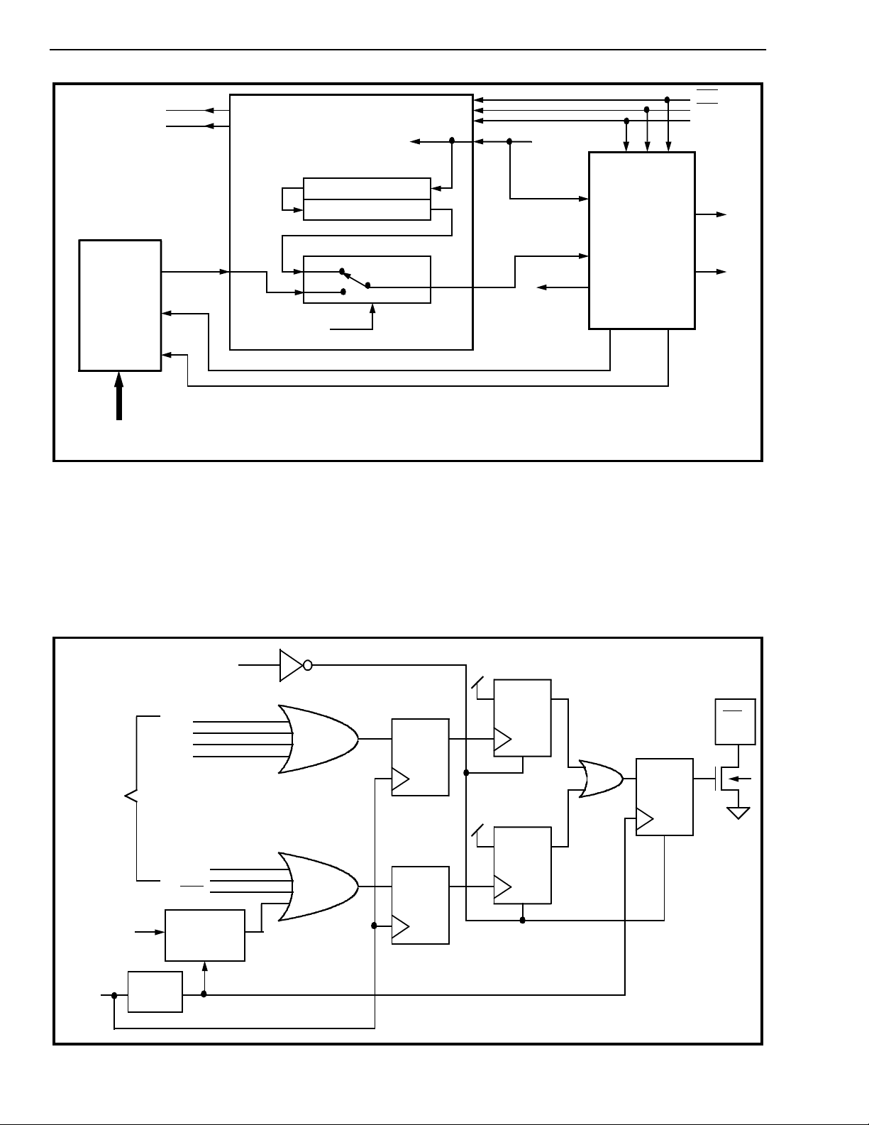
PCW FDLEn = 1 - Transmission of a Bit-ori ented Messag e over the FDL.
PCW FDLEn = 0 - Transmission of an MT8952 (HDLC Controller) as sem bled message-o rie nted signal over the FDL.
CSTo
1SEC
FDLi
MT8926
To PMAC Control
TxBOM
0
1X1X1X1X1X1X101
2 TO 1 MUX
FDLEn
CSTi1
FDLo
From System
Control
CSTi1
TxFDL
TxFDLCLK
RxFDL RxFDLCLK
MT89 76/77
Figure 7 - T 1.40 3/40 8 FDL Mess age Transmis sio n
8 kHz Contro l
Figure 9 illustrates a typical MT8976/77 - MT8926
application. This diagram shows E8Ko (an 8 kHz
output aligned with the received framing bit) of the
INTA
Group 2
SEI*
FSI
CSI
BSI
INTERRUPT
SOURCES
From
Snap-shot
registers
Group 1
RAI
MT8976/77
MT8976/77
SLIP
ALRM
SYN
Toggle
Detector
R
T1 framer connected to E8Ki of the PMAC. The
PMAC uses this signal for frame alignment,
therefore, the 8kHSel (Mast er Control Word 1) of the
MT8976/77 must be active for the framer - PMAC
combination to function properly, even if the interface
is in master mode. See the MT8976/77 data sheet.
V
DD
DQ
DQ
R
DQ
V
DD
R
DQ
DQ
R
IRQ
Delayed
Frame
Pulse**
4-16
Delay
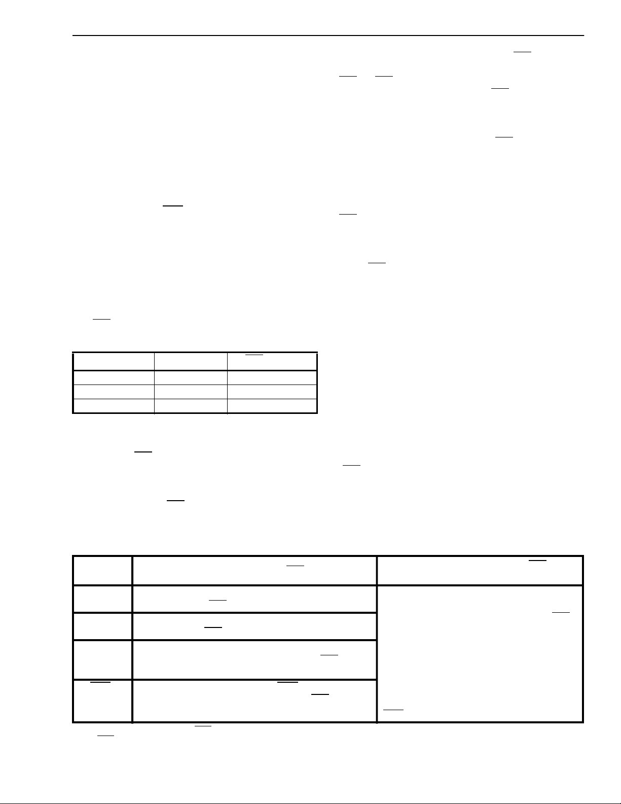
* SEI is reset to 0 when INTA = 0.
** Delayed Frame Pulse occurs during Bit 7 of ST-BUS Channel 1.
Figure 8. Functional Schematic of Interrupt Mechanism
Page 15
MT8926
In slave or loop-timed operation 8KEn of the PMAC
Control Word (Table 14, CSTi1 channel 11 bit 2) will
be high, which will pass the signal on E8Ki through
to E8Ko. In Master mode or if loop-timing is acquired
from another interface, 8KEn must be low, which will
make E8Ko high.
Interrupts
The MT8926 interrupts originate from eight s ources,
which are divided into two groups. Group one (G1)
contains ALRM (SF Yellow Alarm), RAI (ESF Yellow
Alarm), SLIP and SYN
- all except SLIP must be
cleared by some means external to the MT8926.
Group two (G2) contains SEI, FSI, CSI, and BSI these can be cleared via the MT8926. See Tables 16
and 17 for further information.
The interrupting mechanism is controlled by the
interrupt acknowledge bit (INTA) of the PMAC control
word (Table 14). The status of the interrupts is output
on IRQ
. This will allow the three valid states
described in Table 15.
State INTA Bit IRQ
Output
Cleared 0 High Impedance
Armed 1 High Impedance
Triggered 1 0
Table 15. Inte rrupt Sta tes
When a G1 interrupt occurs and IRQ goes low
(Triggered), no other G1 or G2 interrupts will affect
. If IRQ is then Cleared and re-Armed, only an
IRQ
active G2 interrupt can Trigger IRQ
low unless the
G1 interrupt has been removed. That is, both the
MT8926 interrupt mechanism and the interrupting
source of a group must be cleared before a further
interrupt of that group can cause IRQ
to go low. The
only exception to this is SEI, which can be cleared by
INTA ( see Table 11).
A PMAC interrupting signal is either a low-to-high
transition or a change in state (SLIP), therefore, for
to go low t he MT8926 must be Armed before the
IRQ
initiating edge occurs. In the case where all
interrupts are quiescent and then an interrupt
becomes active, while the MT8926 is in its Clear
state, IRQ
will remain in a high impedance condition.
This is true even if the MT8926 is then put in the
Armed state and the interrupt persists (see Figure 8).
It should be noted that when an SF mode T1 signal is
being received the MT8926 CRC error counter will
be incremented once every two superframes (24
.
frames or 3 msec.). This is because SF mode T1 has
no CRC bits. Therefore, the CRC circuitry of the
MT8976/77 will compare the calculated CRC
remainder with th e received F S bits, wh i ch will res ult
in a mismatch. This will increment the MT8976/77
and MT8926 CRC error counters.
In the Cleared state (INTA = 0) interrupt sources are
ignored and IRQ
will always be high impedance. If
the interrupts are not being used, then I NTA should
remain in the Cleared state. When the MT8926 is in
the Armed state and an interrupt occurs, it will go to
the Triggered state (IRQ
Signal
‡
= 0).
To Trigger interrupt (IRQ low)
ALRM ALRM bit low to high AND other G1 interrupts
quiescent AND IRQ
high impedance.
RAI RAI bit low to high AND other G1 int errupt s
quiescent and IRQ
high impedance.
SLIP CSTi0/CSTo Channel 15 Bit 1 (SLIP) changes state
AND other G1 interrupts quiescent AND IRQ
impedance.
†
SYN
CSTi0/CSTo Channel 15 Bit 0 (SYN) low to high
AND other G1 interrupts inactive AND IR Q
impedance.
‡ G1 interrupts are cleared when SYN, ALRM, and RAI = 0.
† The SYN
Note: AND de no te s a l og ic al a nd .
interrupt indicates that a LOS or a AIS condition may exist.
Table 16. Group One (G 1) Int erru pt Activa tion and C leari ng
The MT8926 CRC error counter will count to 255 and
then overflow to zero, which will cause an interrupt
). Therefore, when an SF mode T1 signal is
(IRQ
being received an interrupt will be asserted every
256 X 3 msec. = 768 msec. This can be avoided by
clearing the CRC error counter before it overflows. A
change of state of the 1SEC output (once every 0.5
seconds) can be used to trigger a high-to-low
To Clear and Arm inte rrup t
(IRQ high
impedance)
The INTA bit of the PMAC Control Word
(CSTi1 channel 11 bit 1) should be made
low to clear the interrupt mechanism (IRQ
high impedance). All G1 inter rupts must be
quiescent and then INTA must be made
high
high before a further interrupt can be
generated from G1.
See MT8976/77 data sheet master status
high
word 1 for informat ion on the SLIP and
bits.
SYN
4-17
Page 16

MT8926
transition of the CRCR bit (CSTi1 channel 11 bit 5,
PMAC Control Word). This will ensure the CRC error
counter never overflows.
SLIP and SYN
The MT8976 SLIP and SYN
the PMAC via the MT8976/77 CSTo to PMAC CSTi0
connection. A MT8926 interrupt will be initiated when
the SLIP bit of the framer changes state. This is the
only interrupt source that does not have to be
cleared before another interrupt of that group can
make IRQ
a high impedance condition after a SLIP interrupt
and all other G1 interrupts are quiescent, any G1
interrupt c a n m a ke IRQ
Interrupts
status bits are passed to
go low. Therefore, when IRQ is returned to
to go low.
A Low-to-High transition of the MT8976/77 SYN
will initiate a PMAC interrupt. This loss of
synchronization situation may indicate that a loss of
signal condition (LOS) exist s or that an all ones (AI S
or Blue Alarm) is being received. Therefore, the SYN
interrupt service routine should check the state of t he
AIS and LOS bits of CSTo.
bit
‡
Signal
SEI SEI bit low to high AND other G2
FSI FSI bit low to high AND other G2
CSI CSI bit low to high AND other G2
BSI BSI bit low to high AND other G2
‡ G2 interrupts are cleared when SEI, FSI, CSI and BSI = 0.
Note: AND de no te s a l og ic al a nd .
To Trigger interrupt (IRQ low) To Clear and Arm interrupt (IRQ high impedan ce)
interrupts quiescent AND IRQ
high impedance.
interrupts quiescent AND IRQ
high impedance.
interrupts quiescent AND IRQ
high impedance.
interrupts quiescent AND IRQ
high impedance.
Table 17. Group Two (G2) Interrupt Activation and Clearing
The INTA bit of the PMAC Control Word (CSTi1 channel 11 bit
1) should be made low to clear the interrupt mechanism ( IRQ
high impedance). All G2 interrupt s must be clear and INTA
must be high before a further interrupt can be generated from
G2.
The SEI bit will remain cl ear as long as the INTA bit is low. SEI
can also be cleared (low) by toggling SER (CSTi1 channel 11 bit
7) from high to low.
FSI is cleared (low) by toggling FER (CSTi1 channel 11 bit 6)
from high to low.
CSI is cleared (low) by toggling CRCR (CSTi1 channel 11 bit 5)
from high to low. Valid for ESF only.
BSI is cleared (low) by toggling BPVR (CSTi1 channel 11 bit 4)
from high to low.
4-18
Page 17
MT8926
A
AAAA
AAAA
AAAA
AAAA
AAAA
AAAA
AAAA
AAAA
AAA
Applications
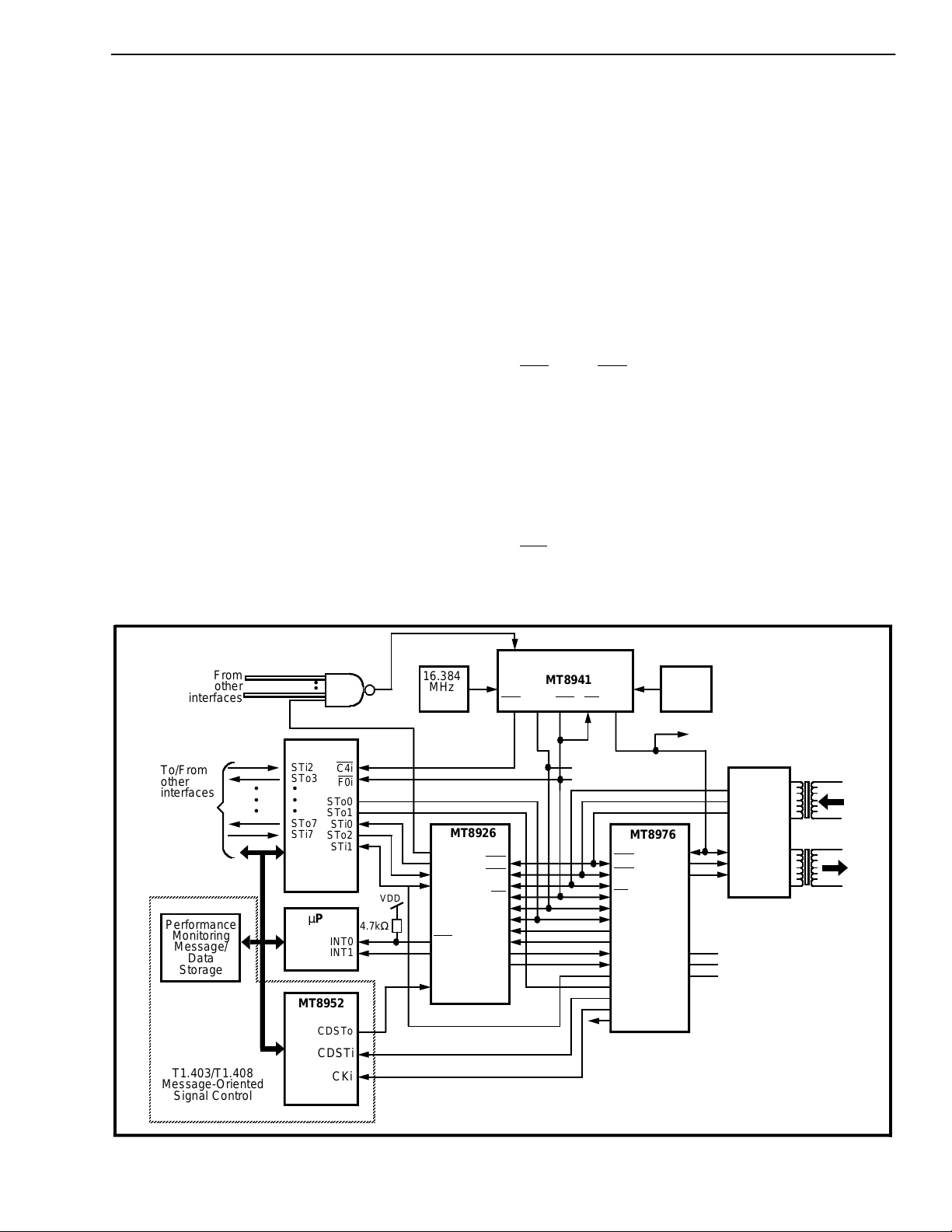
Figure 9 illustrates a typical application of a MT8926
PMAC. T1 data is transmitted and received using a
generic Line Interface Unit (LIU). The LIU passes the
received data and extracted clock to both the
MT8926 and MT8976. E8Ko (MT8976) is derived
from E1.5i by dividing it by 193 and aligning the
result with the receive framing. E8Ko (MT8976)
connects to E8Ki (MT8926), and is used by the
MT8926 for frame alignment. E8Ko (MT8926) is
connected to C8Kb of the MT8941. In MT8941
normal mode, C8Kb is the reference clock for the STBUS and transmit signals (F0, C4 and C2). This 8
kHz output can be turned off (output high) at the
MT8926 so the MT8941 reference clock can be
derived from another interface. The intrinsic jitter
(typical 0.07 UI) and jitter attenuation of the MT8941
will meet T1.408 requirements (see MT8941 data
sheet).
Control of the MT8926 is accomplished over the
CSTi1 ST-BUS stream, which is shared by the
MT8926 and MT8976. Status data (Performance
Monitoring Information) is inserted int o the MT8976
CSTo stream by the MT8926 and is output on its
CSTo stream. This CSTo stream data is routed
through the MT8980 switch, in message mode, to the
microprocessor. The microprocessor will assemble
the information section of the T1.403/T1.408
message-oriented signal and pass it to the MT8952
HDLC controller for transmission over the facility
data link. The MT8952 must be in external timing
mode and will be clocked by the RxFDLCLK output
to the MT8976. The assembly and transmission of
the message-oriented signal is under control of the
1SEC output of the MT8926.
Bit-oriented messages are also transmitted and
received via MT8980 message mode access to the
CSTi1 and CSTo stream s. The MT8926 will receive
bit-oriented messages from the receive T1 line (i.e.,
and RxB). Both bit-oriented and message-
RxA
oriented signals are transmitted over the MT8926
FDLo to MT8976 TxFDL link.
Payload loopback is performed by internally
connecting DSTi1 to DSTo of the MT8926 (under
control of the CSTi1 stream), instead of the normal
connection o f DSTi0 to DSTo ( see Figure 6).
is an open drain interrupt output that will signal
IRQ
the microprocessor when an exception condition
occurs (see Figure 8). Exception conditions are
From
other
interfaces
To/From
other
interfaces
Performance
Monitoring
Message/
Data
Storage
T1.403/T1.408
Message-Oriented
Signal Control
C8Kb
•
•
16.384
MHz
Osc.
MT8941
C2o F0b F0i CVb
C4b
MT8980
STi2
C4i
STo3
•
•
•
•
•
•
STo7
STi7
µP
F0i
STo0
STo1
STi0
STo2
STi1
INT0
INT1
4.7kΩ
VDD
MT8926
E8Ko
CSTo
DSTi0
DSTi1
IRQ
1SEC
FDLi
RxA
RxB
ECLK
F0i
C2i
CSTi1
E8Ki
CSTi0
FDLo
DSTo
MT8952
CDSTo
To other
}
Interfaces
RxA
RxB
E1 5i
F0i
C2i
CSTi1
E8Ko
CSTo
TxFDL
DSTi
DSTo
CSTi0
RxFDL
RxFDLCLK
TxFDLCLK
MT8976
C1.5i
RxSF
TxSF
12.352
MHz
Osc.
TxA
TxB
XCtl
To other T1
Interfaces
Line
Interface
Unit
(LIU)
T1
Receive
T1
Transmit
CDSTi
CKi
Figure 9 - Ty pical T1.403/T1.408 Application
4-19
Page 18

MT8926
counter overflows and alarms. Interrupts are reset
via the PMAC Control Word of the CSTi1 control
stream.
T1.403/408 FD L Me ssag e Transfer Ov ervi ew
ANSI standards T1.403 and T1.408 define an ESF
mode Facility Data Link (FDL), which is used to
transport performance information and control
signals across a T1 link. The FDL channel is formed
from the framing bit position of every second fram e,
and therefore, has a 4 KBit/sec. bandwidth. See
Table 18 for the ESF Framing Pattern.
FRAME # FPS FDL CRC
1X
2CB1
3X
40
5X
6CB2
7X
80
9X
10 CB3
11 X
12 1
13 X
14 CB4
15 X
16 0
17 X
18 CB5
19 X
20 1
21 X
22 CB6
23 X
24 1
Table 18. ESF Frame Pattern
The following two FDL message formats are defined
in T1.403/408:
1) Bit-oriented, which are repeated 16 bit patterns
or codeword messages, and
message consists of a 16 bit codeword of the form
11111111 0XXXXXX0. Therefore, there are 64 unique
codewords or messages def ined by XXXXXX. Refer
to T1.403 or T1.408 for a list of messages and
mes sag e rest ri ct ion s.
BOMs are further divided into priority messages, and
command and response messages. Priority
messages indicate the existence of a serviceaffecting failure, and are repeated until the condit ion
that caused the message is removed. These BOMs
are transmitted f or at least one second, but may be
interrupted as often as once per second, for a
maximum of 100 msec. This is to accommodate the
periodic transmission of message-oriented
performance reports .
Command and response messages are used to
perform various functions, which include the
following:
1) line and payload loopback control,
2) protection switch control,
3) synchro n iz a tion control,
4) reserved for network use, and
5) unassigned.
Each message consists of a 16 bit codeword of the
f orm 11111111 0XXXXX X0, whic h i s repeated at least
10 times.
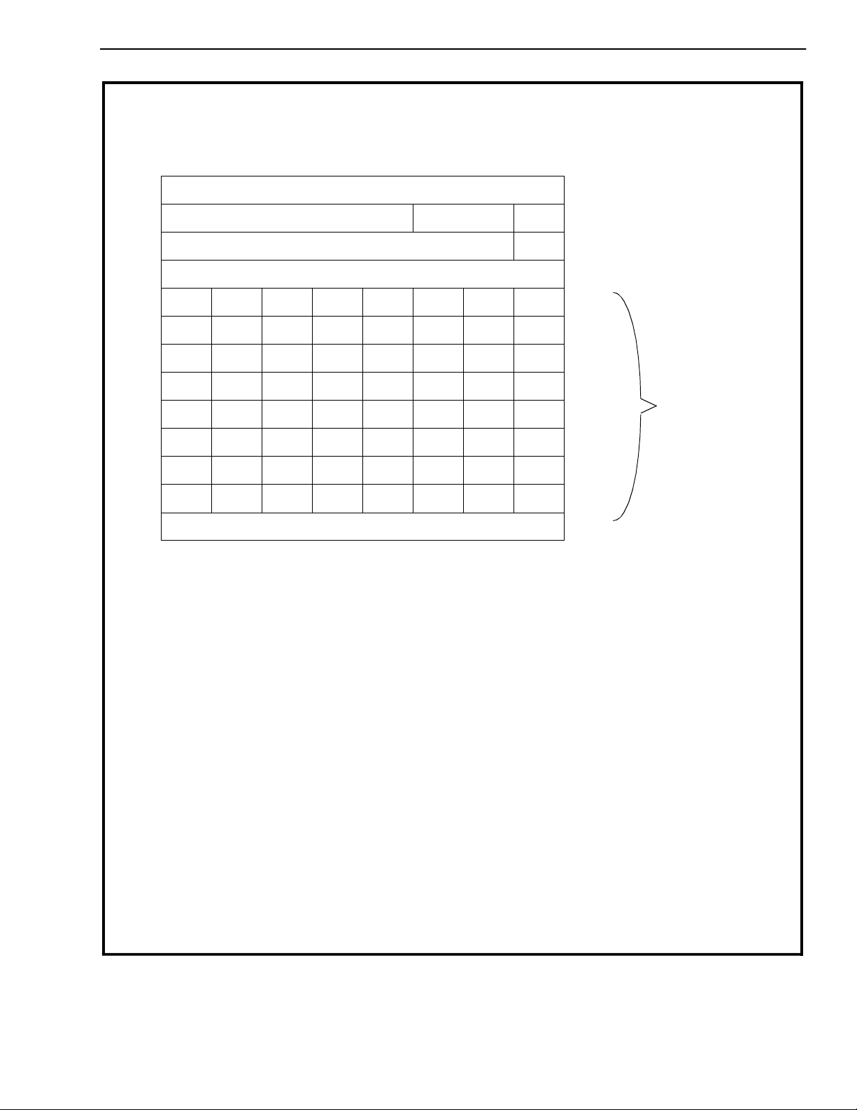
The LAPD message-oriented performance reports
are sent across the FDL once per second using the
bit-assigned message structure of Figure 10. Each
report contains performance data for each second of
the previous four seconds.
When data for the next one second interval t
gathered, it will take the place of t
message. The t
the t
data will move to the t
0-1
data will move to the t
will be discarded. Refer to T1.403 or T1.408 for a
3
data will move to the t
0
position, and the data of t
0-3
data of the last
0
0-1
position, the t
0-2
is
0+1
position,
0-2
more complete definition of this protocol.
0-
2) Message-oriented performance reports, which
are LAPD protocol messages.
Bit-oriented messages (BOMs) are preemptive, and
therefore, override other FDL communications. E ach
4-20
User defined Operations, Administration and
Maintenance (OA&M), terminal-to-network and
terminal-to-terminal communications may also pass
over the FDL.
Page 19
OCTET # OCTET LABEL OCTET CONTENT
87 6 5 432 1
1
FLAG
01111110
MT8926
2
3
4
G3 LV G4 U1 U2 G5 SL G6
5
FE SE LB G1 R G2 Nm NI
6
G3 LV G4 U1 U2 G5 SL G6
7
FE SE LB G1 R G2 Nm NI
8
G3 LV G4 U1 U2 G5 SL G6
9
FE SE LB G1 R G2 Nm NI
10
G3 LV G4 U1 U2 G5 SL G6
11
FE SE LB G1 R G2 Nm NI
12
13
14
ADDRESS
00111000
00111010
00000001
SAPI C/R EA
TEI EA
CONTROL
FCS
INTERPRETATI ON
SAPI = 14, C/R = 0 (CI) EA = 0
SAPI = 14 C/R = 1 (Carrier) EA = 0
TEI = 0, EA = 1
00111000 or 00111010
00000001
00000011
t
}
o
}
to-1
}
t
-2
o
t
-3
}
o
ONE-SECOND REPORT
CONTROL
00000011
ONE-SECOND REPORT
G1 = 1
G2 = 1
G3 = 1
G4 = 1
G5 = 1
G6 = 1
SE = 1
FE = 1
LV = 1
SL = 1
LB = 1
U1, U2 = 0
R = 0
NmNI = 00, 01, 10, 11
FCS
Variable
INTERPRETATION
Unacknowledged Information Transfer
INTERPRETATION
CRC Error Even t = 1
1<CRC Error Event ≤ 5
5<CRC Error Event ≤ 10
10<CRC Error Event ≤ 100
100<CRC Error Event ≤ 319
CRC Error Even t ≥ 32 0
Severely-Errored Framing Event ≥ (FE shall = 0)
Frame Synchroni zatio n Bit Error Event ≥ 1 (SE shall = 0)
Line Code Violation Event ≥ 1
Slip Event ≥ 1
Payload Loopba ck Activated
Under study for synchronization
Reserved (Default value is 0)
One second report modulo 4 counter
INTERPRETATION
CRC 16 Frame Check Sequence
Figure 10 - M essag e -Orien ted Perfor ma nce Re port Stru cture (from T1.40 3 and T1. 408)
4-21
Page 20

MT8926
Absolute Maximum Ratings*
Parameter S ym bol Min Max Units
1 Power Supplies with respect to V
SS
V
DD
2 Voltage on any pi n other than sup plies V
-0.3 7 V
-0.3 VDD+0.3 V
SS
3 Current at any pin other than supplies 40 mA
4 Storage Tem perat ure T
5 Continuous Power Dissipation P
* Exceedi ng these values may cause pe rman ent dama ge . Function al operati on under these co nditi ons is not implie d.
ST
D
Recommended Operating Conditions - Voltages are with respect to ground (V
-40 125 °C
500 mW
) unless otherwise stated.
SS
Characteristics Sym Min Typ‡Max Units Test Con di tions
1 Operating Tem perat ure T
2 Power Supplies V
OP
DD
3 Input High Voltage V
4 Input Low Voltage V
‡ Typical figures are at 25°C and are for design aid only: not guaranteed and not subject to production testing.
-40 85 °C
4.5 5.0 5.5 V
2.4 V
IH
V
IL
SS
DD
V Noise margin = 150 mV
0.4 V Noise margin = 400 mV
DC Electrical Characteristics - Clocked operation over recommended temperature ranges and power supply voltages.
Parameters Sym Min Typ
1 Supply Current I
2 Input High Voltage V
3 Input Low Voltage V
4 Input Leakage Curren t I
5 Output High Current I
6 Output Low Current I
‡ Typical figures are at 25°C and are for design aid only: not guaranteed and not subject to production testing.
DD
IL
OH
OL
2.25 V
IH
V
IL
SS
8mAV
8mAV
‡
Max Uni ts Test Conditions
5 mA Outputs Unloaded
DD
V
0.8 V
±10 µA Digital Inputs
=0 to V
V
IN
OH
OL
DD
=2.4V
=0.4V
AC Electrical Characteristics† - Capacitance
Parameters Sym Min Typ
‡
Max Units Test Conditions
.
1 Input Pin Capacitance C
2 Output Pin Capacitance C
‡ Typical figures are at 25°C and are for design aid only: not guaranteed and not subject to production testing.
Timing is over recommended temperature ranges and power supply voltages.
†
I
O
10 pF
10 pF
AC Electrical Characteristics† - DS1 Link Timing (Figure 11)
Parameters Sym Min Typ
1 Receive Data Setup Time t
2 Receive Data Hold Time t
3 Extracted Clock Width t
4 Extracted 1.5 MHz Clock Period t
† Timing is over recommended temperature & power supply voltage ranges.
‡ Typical figures are at 25°C and are for design aid only; not guaran teed an d not subject to producti on testing
4-22
RS
RH
ECW
P1.5
0ns
30 ns
250 324 ns
500 649 ns
‡
Max Uni ts Test Conditions
.
Page 21
MT8926
Received T1 Link
Bit Cells
RxA
, RxB
ECLK
2.25V
0.8V
2.25V
0.8V
t
ECW
BIT CELL
t
RS
t
P1.5
t
RM
t
ECW
Figure 11 - Receive T1 Link Timing
AC Electrical Characteristics† - 8 kHz Timing (Figures 12)
Parameters Sym Min Typ
1 8kHz Propogation Delay t
2 8kHz Setup Time t
3 8kHz Input Low t
4 8kHz Input High t
† Timing is over recommended temperature & power supply voltage ranges.
‡ Typical figures are at 25°C and are for design aid only; not guarantee d and not subje ct to producti on testing
8PD
8S
8IL
8IH
45 ns
0.065 78 µs
‡
Max Units Test Conditio ns
20 ns 50 pF load
47 µs
.
DATA
ECLK
E8Ki
E8Ko
2.25 V
0.8V
2.25 V
0.8V
2.4 V
0.4 V
Chan nel 2
Bit 1
t
t
8PD
• • • • • •
8S
t
8IL
Channel 17
Bit 2
t
8S
t
8PD
Figure 12 - 8kHz Extracted Framing Signal
t
8IH
Chan nel 2
Bit 1
4-23
Page 22
MT8926
AC Electrical Characteristics† - 2048 kBit/s ST-BUS Streams (Figures 13 and 14)
Parameters Sym Min Typ
1 Clock to Output Delay
2 ST-BUS S et up Time t
3 ST-BUS Hold Time t
4 Serial Output Delay
† Timing is over recommended temperature & power supply voltage ranges.
‡ Typical figures are at 25°C and are for design aid only; not guarantee d and not subje ct to producti on testing
Note➀ - The PMAC is overwriting some of the bits received on CSTi0, and transmitting the aggregate on CSTo. Line loopback codes
are being transmitted on DSTo.
②
- The ST-BU S s tr e am be ing r e c eiv e d o n C STi0 i s n ot being ov er w ritten, but pa s se s through th e P MAC unalte r ed . D S Ti0 an d
Note
DSTi1 are not overwritten, but passes through the PMAC unaltered to the DSTo output.
2.25 V
C2i
0.8V
➀
②
t
COD
STS
STH
t
SOD
15 ns
50 ns
BIT CELL BOUNDARIES
‡
Max Uni ts Test Conditions
125 ns 150 pF load
35
15
40
ns 150 pF load CSTo
50 pF load CSTo
150 pF load DSTo
.
CSTo, DSTo
CSTi0/1
DSTi0/1,
CSTi0
DSTo, CSTo
2.4V
0.4V
2.25 V
0.8V
2.25V
0.8V
2.4V
0.4V
t
COD
t
STS
t
STH
Figure 13 - ST-BUS Timing - CSTo/DSTo Altered by PMAC
t
SOD
t
COD
4-24
Figure 14 - ST-BUS Timing - CSTo/DSTo Un altered by PMAC
Page 23
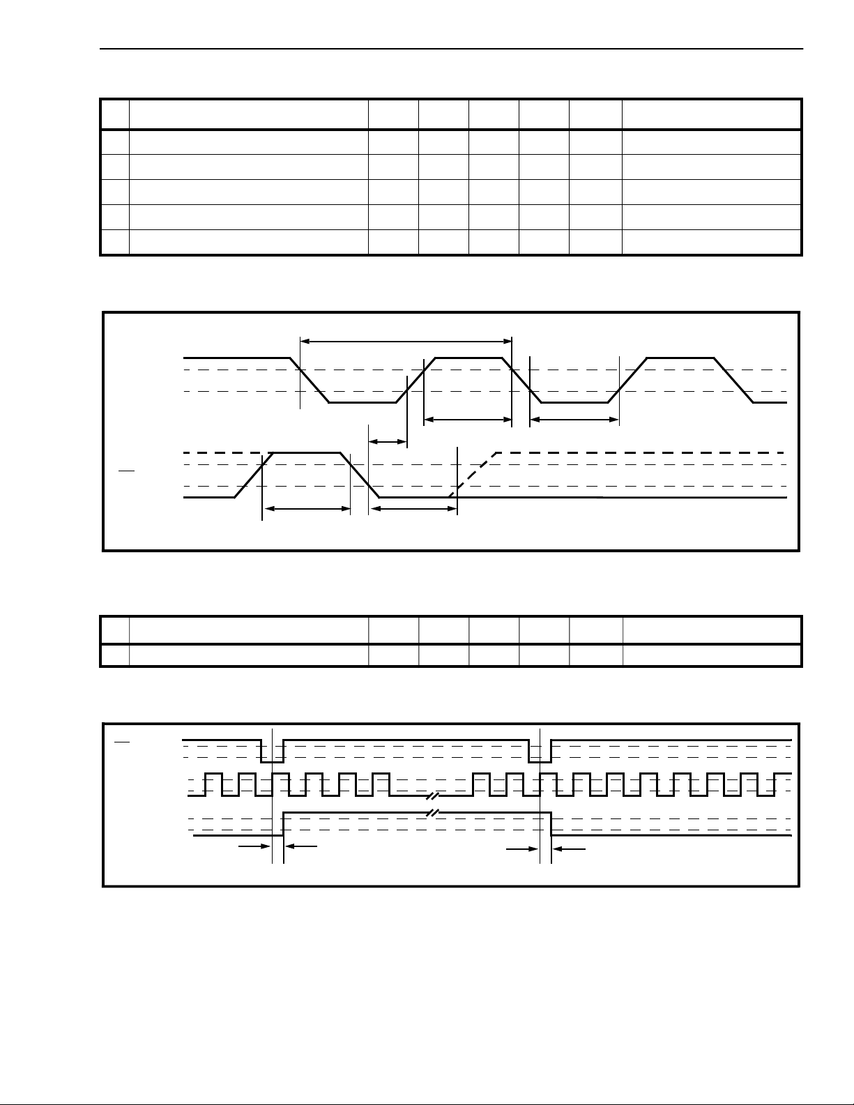
AC Electrical Characteristics† - Clock and Frame Pulse Timing (Figure 15)
Parameters Sym Min Typ
‡
Max Units Test Conditions
MT8926
1 C2i Clock Period t
2 C2i Clock Width High or Low t
3 Frame Pulse Setup Time t
4 Frame Pulse Width High t
5 Frame Pulse Width Low t
† Timing is over recommended temperature & power supply voltage ranges.
‡ Typical figures are at 25°C and are for design aid only; not guarantee d and not subje ct to producti on testing
2.25V
C2i
0.8V
2.25V
F0i
0.8V
t
FPH
2P
2W
FPS
FPH
FPL
t
2P
t
FPS
400 488 600 ns
200 244 300 ns
50 ns
50 ns
50 ns
t
2W
t
FPL
t
2W
.
Figur e 15 - ST-BU S Cl ock and Fr ame P uls e Tim ing
AC Electrical Characteristics† - 1SEC Output Timing (Figure 16)
Parameters Sym Min Typ
1 1SEC Output Delay t
† Timing is over recommended temperature & power supply voltage ranges.
‡ Typical figures are at 25°C and are for design aid only; not guarantee d and not subje ct to producti on testing
2.25V
F0i
0.8V
2.25V
C2i
0.8V
2.4V
1SEC
0.4V
t
1SD
1SD
Figure 16 - 1SEC Timing
‡
Max Units Test Conditions
95 ns 150 pF load
t
1SD
.
4-25
Page 24
MT8926
CSTi0/1
C2i
Frame n Frame n + 1
Ch 0 Ch 1 Ch 11 Ch 12
10 7 6 2 1*07 6* *
t
IOD
IRQ
INTA Bit. IRQ
*
**
Condition initiating interrupt
Note:
t
(IRQ Output Delay) is dependent on the IRQ pull-up resistor.
IOD
High Z
is returned to High Z by INTA=0, INTA=1 in the previous frames. This can occur in frame n+1 or in a later frame.
Active Low
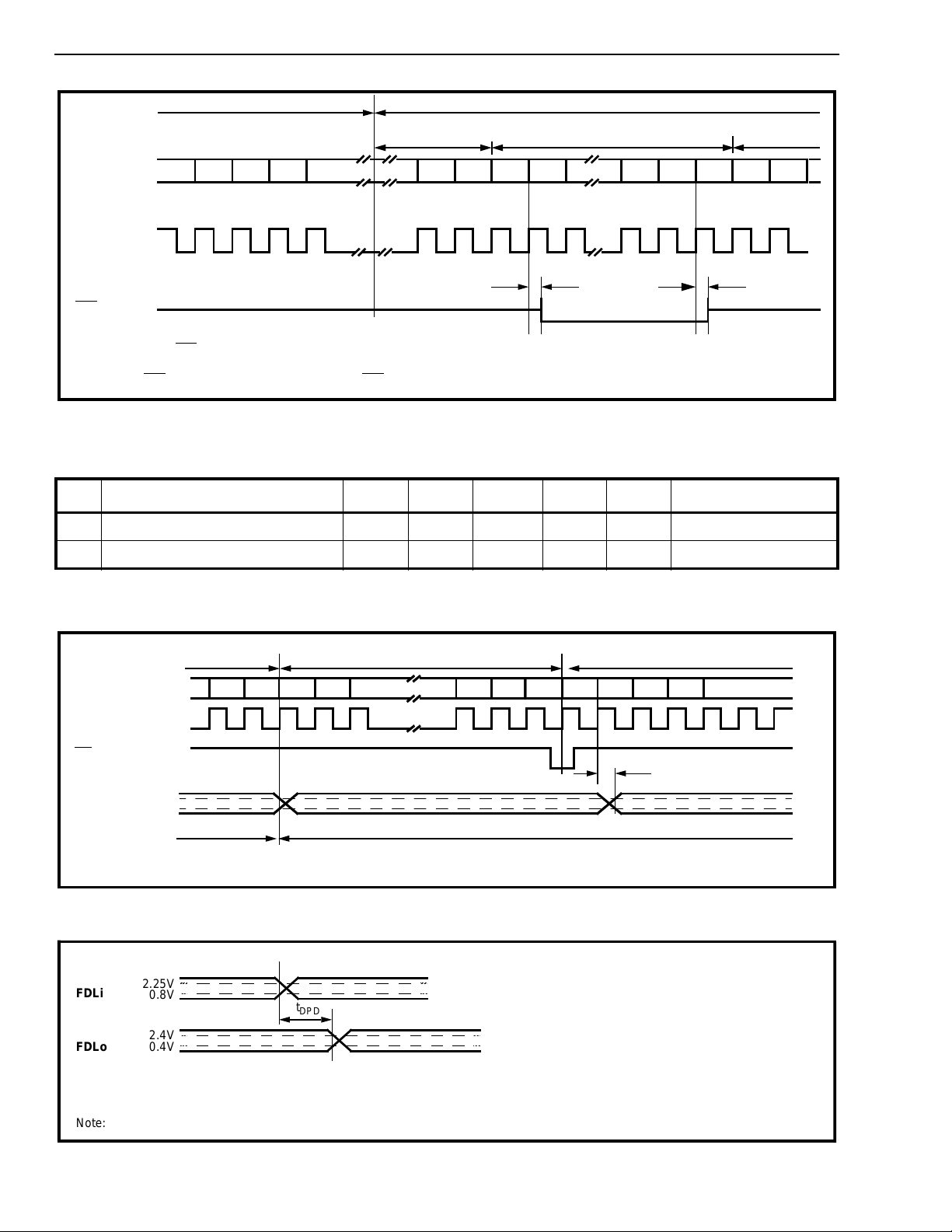
Figure 17 - Interrupt Functional Timing
AC Electrical Characteristics† - Facility Data Link Timing (Figures 18 and 19)
Parameters Sym Min Typ
1 Data Link Output Delay t
2 Data Link Propagation Delay t
† Timing is over recommended temperature & power supply voltage ranges.
‡ Typical figures are at 25°C and are for design aid only; not guarantee d and not subje ct to producti on testing
Ch 11 Ch 12 Ch 31 Ch 0
1*76 2107654
C2i
DOD
DPD
‡
Max Units Test Conditions
45 ns 150 pF load
40 ns 150 pF load
.
t
IOD
High Z
F0i
FDLo
*FDLEn = 1, FDLEn=0 in the previous frames.
2.4V
0.4V
FDLi Data
Figure 18 - FDL Bit-o rien ted Mess ag e Timing
FDLi
FDLo
Note: FDLEn = 0
2.25 V
0.8V
2.4V
0.4V
Figure 19 - FDL Message-oriented Signal Tim ing
4-26
t
DPD
TxBOM Data
t
DOD
Page 25

MT8926
Appendix
Control and Status Register Summary
76543210
Debounce
1 Disabled
0 Enabled
TSPZCS
1 Disabled
0 Enabled
B8ZS
1 B8ZS
0 Jammed
Bit
8KHSel
1 Disabled
0 Enabled
XCtI
1 Set High
0 Cleared
ESFYLW
1 Enabled
0 Disabled
Robbed Bit
1 Disabled
0 Enabled
YLALR
1 Enabled
0 Disabled
Master Control Word 1 (Channel 15, CSTi0)
RMLOOP
1 Enabled
0 Disabled
DGLOOP
1 Enabled
0 Disabled
ALL 1’s
1 Enabled
0 Disabled
ESF/D4
1 ESF
0 D3/D4
Reframe
Device
Reframes on
High to Low
Transition
SLC-96
1 Enabled
0 Disabled
CRC/MIMIC
See Note 1
Maint.
1 4/12
0 2/4
Master Control Word 2 (Channel 31, CSTi0)
Data
1 Enabled
0 Disabled
UNUSED - KEEP AT 0
Polarity
1 No Inversion
0 Inversion
Loop
1 Ch. looped
back
0 Normal
Per Chan nel Co ntro l Words (A ll Chan nels on CS Ti0 Excep t Chan nel s 3, 7, 11, 15, 19, 23 , 27 and 31)
Transmitted
First
TxBOM
Transmitted
Last
Transmit Bit-Ori ented Mes sage R egister (Chan nel 7, CSTi1)
SER
High-to-Low
Reset
FER
High-to-Low
Reset
CRCR
High-to-Low
Reset
BPVR
High-to-Low
Reset
1 F
0 F
FSel
, FT, FPS
S
only
T
8KEn
1 Enabled
0 Disabled
INTA
1 Enabled
0 Disabled/
Clear
FDLEn
1 TxBOM-to-
FDL
0 FDLi-to-FDLo
PMAC Control Word (Channel 11, CSTi1)
00 Normal
UNUSED
01 Payload
10 LL Enable
11 LL Disable
Loopback Control Word (Channel 15, CSTi1)
UNUSED - KEEP AT 0
A
Txt. Sig. Bit
B
Txt. Sig. Bit
C
Txt. Sig. Bit
D
Txt. Sig. Bit
Per Chan nel Co ntro l Words (A ll Chan nels on CS Ti1 Excep t Chan nel s 3, 7, 11, 15, 19, 23 , 27 and 31)
CHANNEL COUNT BIT COUNT
Phase Sta tus Word (Cha nnel 3, CSTo)
4-27
Page 26

MT8926
Appendix (continued)
Control and Status Register Summary
7654 3 2 1 0
LLDD
1 Detected
UNUSED
0Not
Detected
LLED
1 Detected
0Not
Detected
FECV
1 In-Sync
0 Out-of-Sync
TMR
Changes
State
once
per second
PMAC Mis cel la ne ous Sta tu s Wor d (C ha nn el 7 , C STo)
CRC ERROR COUNT
Cyclic Redundanc y Check-6 Error Co unter (Ch annel 11, CSTo)
YLALR
1 Detected
0Normal
MIMIC
1 Detected
0Not
Detec t e d
ALRM
1 Detected
0Not
Detec t e d
RAI
1Detected
0Not
Detected
MFSYNC
1 Not Detected
0 Detected
LOS
1 Detected
0Normal
SLIP
Changes
State
when Slip
Performed
Master S tatus Wo rd 1 (Chan nel 15, C STo)
SEVERELY ERRORED FRAMING EVENT COUNTER (SE) FRAMING ERROR COUNTER (FE)
Severely E rrored Fram ing Even t and Error Co unte rs (Cha nne l 19, CSTo)
BOMV
1 Valid
0 Invalid
SYN
1 Out-of-Sync.
0 In-Sync
BPV ERROR COUNT
Bipolar Violation Error Counter (Channel 23, CSTo)
Received
First
RxBOM
Receive B it-Or ien ted Mess ag e Reg ister (Ch ann el 27, CSTo)
BlAlm
1 Detected
0Not
Detec t e d
FrCnt
Frame
Count
XSt
1XSt High
0 XSt Low
SEI
1 SE Toggles
0 SER High-
to-Low
FSI
1 FE F-to-0
0 FEF High-
to-Low
CSI
1 CRC FF-
to-00
0 CRCR High-
to-Low
BSI
1 BPV FF-to-
00
0 BPVR High-
to-Low
Master S tatus Wo rd 2 (Chan nel 31, C STo)
UNUSED
A
Rec’d. Sig. BitBRec’d. Sig. BitCRec’d. Sig. BitDRec’d. Sig. Bit
Per Channel Status Word (All Channels on CSTo Exc ept Channels 3, 7, 11, 15, 19, 23, 27, 31)
Note 1: In ESF m o de :
In D3/D4 mode:
1: CRC calc. ignored during Sync.
0: CRC checked for Sync.
1: Sync. t o first cor rec t S - bi t p at tern .
0: Will no t Sync. if Mim ic d ete c ted.
Received
Last
AIS
1 Detected
0Not
Detected
4-28
 Loading...