

Page 1

ISO-CMOS ST- B US FAMILY
MT8950
Data Codec
Features
• Transparent cod ing an d de codin g of 0 to 8 , 9. 6
and 19.2 k bps dat a
• Coding com pat ible to PCM voice c hann els at
56/64 kbps in ST-BUS format
• Automatic li ne pol arity det ec tion an d corre ction
• Loopback facility for test purposes
• Selectable data formats: RZ or NRZ
• Eight us e r s el ect able modes of operation
• Low power IS O-CM OS te chnol ogy
Applications
• Transparent cod er/dec oder fo r sync hrono us
and async hrono us da ta
• Data terminal (RS-23 2C , etc.) to ST-BUS
inter fac e
• Data switching on digital PBXs
• Channel banks/TD M m u lti ple x ers
ISSUE 4 November 1990
Ordering Information
MT8950AC 24 Pin Ce r am i c D IP
0°C to 70°C
Description
The MT8950 is a coder/decoder which uses the
Transition Encoded Modulation (TEM) technique for
encoding/decoding low speed data to and from a 56/
64 kbps channel (equivalent to PCM Voice). The
coding and decoding scheme is transparent and can
accept either synchronous or asynchronous data up
to 8 kbps (inclusive); at 9.6 kbps and 19.2 kbps.
The MT8950 is fabricated in MITEL’s ISO-CMOS
technology.
DP
SCLK
DR1
D
R
DF
D
X
D
X
RxE
NRZo
SPi
Enable
Logic
NRZ/RZ
Output
2
1
2
Circuit
Timing
& Mode
Control
NRZ/RZ
Input
Circuit
Control
Register
PRST
Decoder
Encoder
Monitoring
Interface
V
DD
ST-BUS
Interface
V
SS
C2i
F1i
CA
DSTi
DSTo
CSTi
DA
SPo
Figure 1 - Functional Block Diagram
6-3
Page 2

MT8950 ISO-CMOS
CSTi
DSTi
C2i
DSTo
F1i
CA
DF
RxE
DX1
DX2
NRZo
VSS
1
2
3
4
5
6
7
8
9
10
11
12
24
23
22
21
20
19
18
17
16
15
14
13
VDD
NC
PRST
NC
NC
DR1
DR2
DA
SPo
SPi
DP
SCLK
Figure 2 - Pin Connections
Pin Description
Pin # Name Description
1CSTiControl ST-BUS In (TTL Input) - This ST-BUS interface pin accept s a serial input
stream which loads th e Control Register. The mode of operation of the
device, the bits in the Violation word, and, the resetting of Data Activity (DA
Scan Point output (SPo
are updated once every ST-BUS frame when the interface is enabled.
) are controlled by this register. The contents of the register
) and
2DSTiData ST-BUS I n (TT L Input) - Accepts the 8 bits of TEM Data when the ST-BUS
interface is enabled.
3C2i2.048 MHz Clock (TTL Input) - This is the input for the 2.048 MHz clock.
4 DSTo ST-BUS Output (Three-State Output) - This is the 2.048 Mbps serial output for
theTEM encoded word. It is enabled when both F1i
5F1i
Framing Type 1 Input (TTL Input) - This active low input, in conjunction with CA,
and CA are low.
enables the ST-BUS interface (DSTi, DSTo and CSTi). It is internally sampled on
every positive edge of the C2i clock and provides frame synchronization.
6CA
Control Address (TTL Input) - This active low input (in conjunction with F1i)
enables the ST-BUS interfa c e.
7DFData Format Select (CMOS In pu t ) - When HIGH, the Data Code c accepts and
delivers the data in unipolar Return to Zero (RZ) format. When LOW, the data
format is unipolar NRZ.
8RxE
9D
1Data Transmit 1 (Schmitt Input) - If DF= LOW , accepts data in the NRZ format.
X
Received Energy Signal (Schmitt Input) - When RxE goes LOW it establishes the
polarity of the input pins D
last pulse before RxE
also enables the operation of DA
and 6) of the codec, RxE
condition. RxE
should be exerted LOW for the duration of a data call.
1 and DX2 in the RZ mode. The input which received the
X
goes LOW is established as the unipolar MARK input. RxE
and SPo outputs the loopback modes (Modes 4, 5
is forced to the LOW state internally independent of the pin
(HIGH = MARK, LOW = SPACE).
If DF=HIGH, accep ts active low unip olar pulses re presenting the dig ita l data in t he
RZ format. MARK or SPACE polarity is established by the RxE
input.
6-4
Page 3

ISO-CMOS MT8950
Pin Description (continued)
Pin # Name Description
10 DX2 Data Transmit 2 (Schmitt Input) - If DF = LOW, accepts data puls es which are
encoded only if there is no activity on the D
restrictions on the use of this input is explained in the t ext.
If DF= HIGH, accepts active low unipolar pulses representing the digital dat a in the
RZ format. MARK or SPACE polarity is established by the RxE
1 pin - the data format and
X
input.
11 NRZo
Non-Return to Zero Output (Open Drain Outpu t) - The incoming data, in the RZ
format or the NRZ format , is internally converted to inverted NRZ and appears on
this open drain output. This output in conjunction with the SPi input can be used for
long space detection.
12 V
SS
Ground (0 V olt).
13 SCLK Secondary Clock (TTL Input) - This is an external clock input that determine s the
timing of the Violation Word and the synchronization pul se s. If these features are
not to be utilized, this input can be tied to V
SS
.
14 DP Drive Point Output (To tem -po le Outpu t) - This output is exerted high when the
Control Register bits b7, b6 and b5 are set to 110 (decimal 6). The operation of the
Codec is normal in every other respect.
15 SPi Uncommitted Scan Point Input (V o ltage Comparator Input ) - A LOW to HIGH
16 SPo
transition on this input causes SPo
SPACE condition in conjunction with NRZo
Uncommitted Scan Point Output (Totem-pole Output ) - This output is set LOW
when the SPi input undergoes a LOW to HIGH transition. T h e SPo
to be set LOW. T his is used to detect a long
(pin 11).
is reset by the
presence of a logic "1" in bit b0 of Co ntrol Register. This function is active at all
17 DA
times except when RxE
Data Activity (Totem-pole Ou tput ) - The NRZ/RZ input circuitry monito rs the
is false and during power reset conditions.
input signal (after polarity is established) and activates this output when it detects a
SPA CE on the input. This output is reset by the presence of a logic "1" in bit 1 of the
Control Register. The DA
function is active at all times except when RxE is false and
during power reset conditions.
18 D
2 Data Receive 2 (Totem-pole Output) - If DF = LOW ( NRZ form at ), outputs th e
R
secondary data signal in the NRZ form as explained in the text.
If DF = HIGH (RZ format), outputs unipolar, active high MARK pulses.
19 D
1 Data Receive 1 (Totem-pole Output) - If DF = LOW (NRZ format) , outputs the
R
NRZ data signal. ( HIGH = MARK, LOW = SPACE)
If DF = HIGH (RZ format), outputs unipolar, active low SPACE pulses.
20 NC No connecti on .
21 NC No connecti on .
22 PRST
Power Reset (CMOS Schmitt Input ) - A LOW level on this input evokes the power
reset condition for the cod ec.
23 NC No connecti on .
24 V
DD
Positi ve Sup pl y Voltage +5 volts ± 10% .
6-5
Page 4

MT8950 ISO-CMOS
Theory of Operation
The MT8950 is an encoder/decoder which operates
on low baud rate data (up to 19.2 kbps) to convert it
to the ST-BUS format. The data can subsequently
be transparently switched or transm itted in a manner
identical to PCM encoded voice. In this respect, the
functional characteristics of the device are very
similar to many industry standard voice codecs.
Asynchronous and synchronous data from 0 to 8
kbps and at 9.6 kbps is accepted by the codec
without any restrictions. Asynchronous data at 19.2
kbps should have at least two s top bits for the device
to encode it properly. The data is encoded by the
Codec into an eight bit word which occupies one 64
kbps channel on the ST-BUS. Conversely, it accepts
an encoded 8 bit word from an incoming ST-BUS
stream and regenerates the original digital signal.
Mitel’s ST-BUS is a synchronous time division
multiplexed serial stream with a bit rate of 2048
kbps. In a telecommunications environment, it is
generally divided into 32 channels made up of 8 bits
each, with an effective bandwidth of 64 kbps per
channel. These channels may carry data or PCM
encoded voice.
Low S pee d Da ta For ma t
The Data Codec can accept low speed data in eit her
Non Return to Zero (NRZ) or Return to Zero (RZ)
format. The NRZ format requires only one line to
carry the data. This format is suitable for interfacing
the data codec with RS-232 type terminals and
microprocessor peripherals such as UARTS, ACIAs,
etc. All signals have to be converted to TTL voltage
levels before being input to the codec.
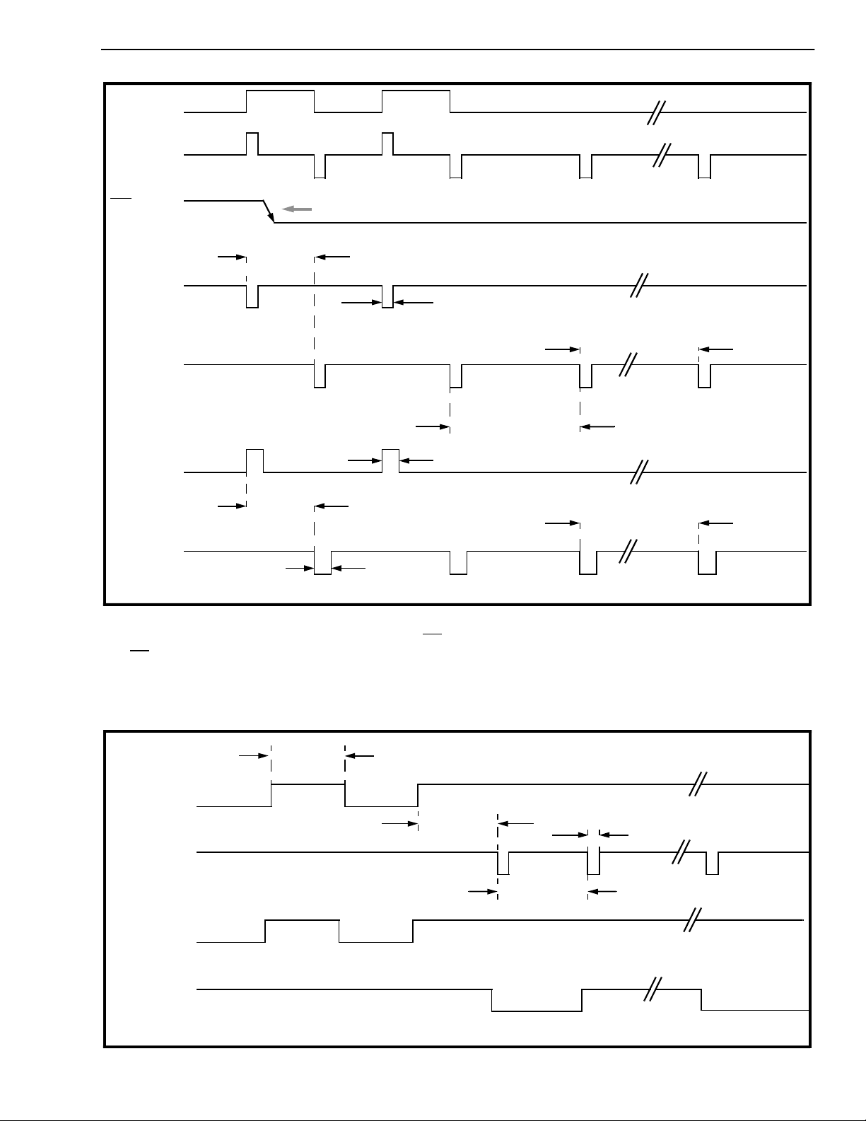
The RZ format requires two separate lines to
represent the MARKs and SPACEs in the data as
illustrated in Figure 4. This format is useful when the
data terminal is located some distance from the
codec and the data is to be transmitted over a line as
a three level signal (a positive pulse for the
beginning of MARKs, negative pulse for the
beginning of SPACEs and zero level for no change in
the signal). The three level signal is converted to its
TTL-Compatible binary form as shown in Figure 4
before being applied to the codec. A pulse appears
on one line of the input indicating the beginning of
MARKs. This is followed by a pulse on the second
line indicating the beginning of SPACEs. If two or
more pulses appear consecutively on the same line
before the second line of the pair receives or
transmits another pulse, then these pulses can be
considered to be v iolating the normal rule of the RZ
format and are called "Violation Pulses". The data
codec will accept these violations with the restriction
that the time differenc e between a violation pulse
Data Rate
Bits/Sec
Asynchronous
Restrictions
Synchronous
Restrictions
Percentage
Distortion
†
0 - 80 00 9600 19200
None None Minimum
2 Stop Bits
None None None
±3.2 ±3.8 ±7.5
Table 1. Summary of Data Codec Capabilities.
† Refers to the maximum distortion in the bit period timing of the
regenerated data. (Channel Bandwidth = 64kbps )
Percentage Distortion = |T
where TBO = Origi na l Da ta Bi t Pe rio d
T
= Regenerated Data Bit Period
BR
BO
- T
BR
| / T
BO
X 100
and an actual data transition be at least 125µs. The
violation pulses can be on the MARK or SPACE line.
In a communications system, these violat ions can be
used to carry other information when no data is
being transmitted.
Encoding/Decoding Scheme
The Data Codec uses a Transition Encoded
Modulation (TEM) technique to encode low speed
data onto a 56 or 64 kbps equivalent PCM voice
channel. This coding algorithm significantly reduces
data bit distortion. The timing distortion in the
regenerated data is summarized in Table 1. A simple
sampling method for encoding the data would
require a 256 kbps channel to obtain the same low
distortion figures.
If the encoded information is to be transmitted over
digital T1/DS1 trunks, the maximum percentage
distortion in the regenerated data is effectively
doubled. This is due to the fact that the least
significant bit in specific channels on these trunks is
used to transmit signalling information. Thus the
bandwidth per channel is reduced to 56 kbps.
The encoder stage of the Data Codec observes
data transitions in discrete timing windows which are
125µs wide. These timing frames are further divided
into 32 timeslots of 3.906µs duration each (see
Figure 3). The position of the first data transition, the
total number of transitions, and, the time period
between the transitions in this 125µs frame is
encoded as an 8 bit word.
The first five bits (b0 to b4) indicate the position of
the first data transition with respect to the 32
timeslots in the window. Bit 7 in the encoded word
represents the absolute value of the data in the 31st
timeslot. Bits 5 and 6 in conjunction with bit 7 are
used to identify the total number of transitions and
the time period between the transitions. Due to the
fixed bit rate restrictions above 8 kbps, a maximum
6-6
Page 5

Internal
Clock
ISO-CMOS MT8950
125 µs
0123456789
-1
b7
#
1
1
1
2
1
b4b3b2b1b
3
1
4
1
5
1
6
1
7
01234 01234567
b1b
0
b4b3b2b1b
0
b4b3b2b1b
b4b3b2b1b
0
0
10
0
22• • •
b4b3b2b1b
Figure 3 - TEM Coding Scheme
(Note: Wavef orm s s ho w n ar e bi po la r RZ equiva le nt of s eparate R Z/ N RZ inputs)
24 25 26 27 28 29 30
b4b3b2b1b0=11111
0
b4b3b
2
b7
31
1
1
0
0
1
1
1
023
0
Frame Type
b5
b6
1
1
1
1
1
1
1
0
1
0
1
0
0
0
#
Frame
Description
Level
b7
†
Frame Type
b6 b5
First Transition
b4 b3 b2 b1 b0
Notes
1 No Pul se 1/0 1 1 1 1 1 1 1
2 2 Data Pulses (T =52 µs ) 1/0 1 1 X X X X X X X X X X ≤ 10001 (17)
3 3 Data Pulses (T =52 µs ) 1/0 1 1 X X X X X X X X X X ≤ 00100 (4)
4 1 Data P u lse 1/0 1 0 X X X X X X X X X X = 0 to 31
5 Violat io n Pulse 1/0 1 0 X X X X X X X X X X = 0 to 31
6 2 Data Pulses (T=104 µs)
1/0 0 1 X X X X X X X X X X > 00011 (3)
(Timeslot 4 to 31)
7 2 Data Pulses (T=104 µs)
(Timeslot 0 to 3)
1/0 0 0 Y Y Y X X XX = 0 to 3
YYY = 0 to 7
Table 2. TEM Coding Summary
† Note: The Level bit (b7) indicates the level (HIGH or LOW) of the input data in timeslot 31 of the current frame.
of seven frames types are possible as shown in
Figure 3. In frame t ype 7, th e fi rs t five bits (b0 to b 4 )
are used to represent two transitions instead of the
normal first transition. Not e that the data transitions
in Figure 3 are shown as a three level signal. A
positive transition indicates the beginning of one or
more continuous MARKs and a negative transition
indicates the beginning of one or more continuous
SPACEs.
The decoder stage regenerates the original data
from the 8 b i t T EM word. T h e a bs o lute values of th e
data signal in the present and previous frames as
given by b7(n) and b7(n-1) are EX-ORed and the
result in combination with the remaining bits of the
TEM word is us ed to reproduce the original data with
an accuracy of ± 3.906µs (see Table 2). Due to the
data speed restriction above 8 kbps, the second and
third transitions (if any) will be reproduced at
6-7
Page 6

MT8950 ISO-CMOS
intervals which are multiples of 52µs (depending
upon the input data baud rate).
Functional Description
The functional block diagram of the data codec is
shown in Figure 1. The low speed data to be
encoded is accepted by the NRZ/RZ input circuitry
and relayed to the encoder. The 8 bit encoded word
is transmitted within one channel time period on to
the ST-BUS serial output stream. At the same time
an 8 bit TEM word is loaded into the decoder via the
incoming ST-BUS stream. The low speed data is
regenerated and output by the NRZ/RZ output
circuitry. The data codec can operate in eight
modes. The specific mode of operation is selected
by programming the internal Control Register using
the CSTi ser i al inp ut.
Transmit Path
The NRZ/RZ input circuitry can be programmed to
accept RZ or NRZ data by asserting the appropriate
level on the DF pin (HIGH=RZ format; LOW=NRZ
format).
In the RZ form at, b oth D
input data. MARK pulses are received on one line
input and SPACE pulses on the other. The MARK
and SPACE polarities of the input pins are fixed by
the high to low transition of the RxE
input having the last transition before RxE
is selected to be the MARK input. Thus to ensure
correct polarity selection, the data codec should be
receiving MARK pulses before RxE
The RxE
line must be kept low for the duration of
the call. As indicated before, t he Data Codec does
accept violation pulses. The violation pulses can be
input on the MARK or SPACE lines. The time
difference between a violation pulse and an actual
data pulse must be at least 125µs . Since only one
violation pulse is encoded per frame, the minimum
time period between consecutive pulses should be
125µs as illustrated in Figure 4.
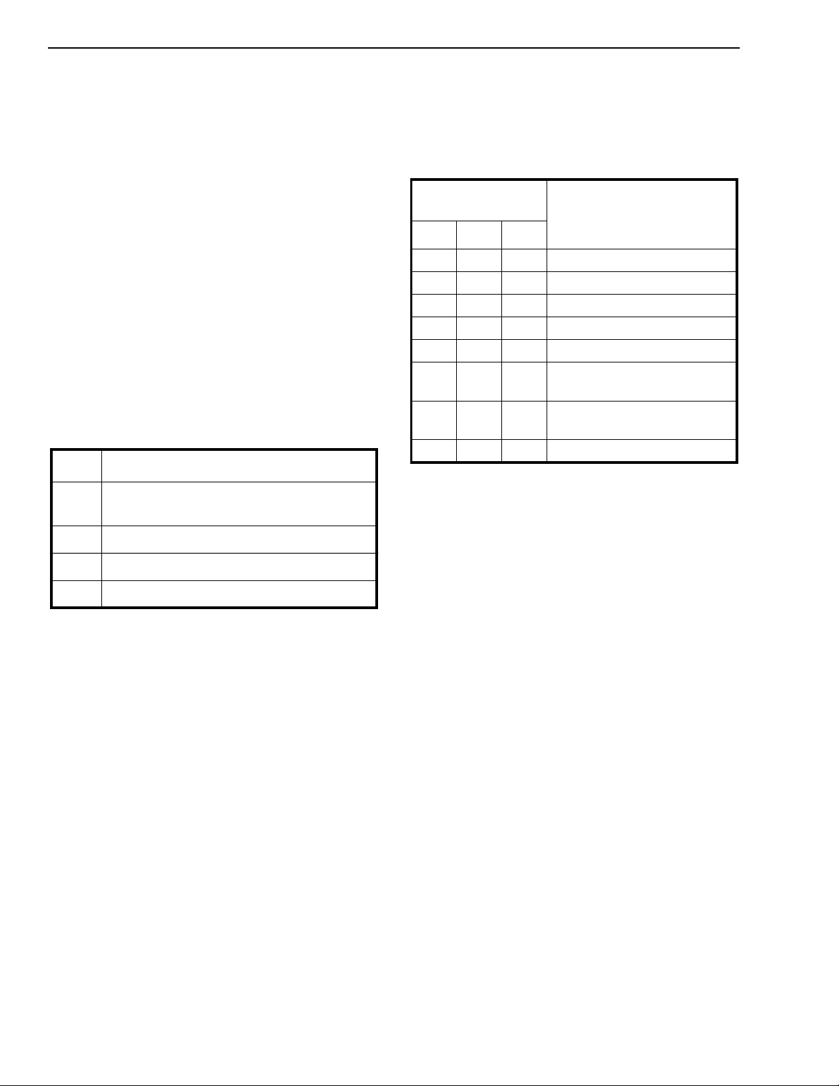
In the NRZ format, only one line is required for the
data. This is input at D
D
2, can be used fo r transmitting secondary control
X
information. The signal on this input pin is encoded
only when there is no activity on the D
during steady MARK or SPACE condition on the data
line. To ensure proper encoder function, the signal
to the D
2 line should be applied after at least 125µs
X
have elapsed since t he last data transition on D
The acceptable data format for the D
illustrated in Figure 5. Each pulse on the line is
1 and DX2 are used for the
X
line. The
goes low
is taken low.
1 (Pin 9). The second input,
X
1 line, i.e.,
X
2 input is
X
1.
X
encoded as a single transition. The minimum time
period bet ween co nsec utive pulses should be 125 µs.
The encoding of the NRZ/RZ data to the TEM format
is performed by the encoder. The 8 bit TEM words
are transmitted on the outgoing ST-BUS channel via
DSTo. This is a three state output which is enabled
only when both CA
and F1i are low (see Figure 11).
Receive Pa th
The 8 bit word generated by a data codec at a
remote end is shifted in from the incoming ST-BUS
stream via the DS Ti input. The word is shifted in at
the same time as the outgoing word is shifted out,
i.e., when both CA
and F1i are low as illustrated in
Figure 11. The NRZ/RZ low speed data is
regenerated by the decoder section and output via
D
1 and DR2.
R
If the chip is operating in the RZ format, D
transmits MARK pulses and D
1 transmits SPACE
R
R
pulses. T he format of the output signal is shown in
Figure 4. The width of an output pulse is nominally
35µs and cannot be altered by the user. Violation
pulses will appear on the line on which they were
initially inserted at the remote end.
In the NRZ format D
output pin D
2, transmits the secondary signal. Each
R
1 outputs the data. The second
R
transition in this signal represents one data pulse
encoded by the rem ote end. An example of the type
of waveform observed is illustrated in Figure 5.
The NRZ/RZ output circuitry also transmits
synchronizing pulses if the data decoded from DSTi
is idling ( i.e., no data trans itions) for mo re than six
clock periods of the Secondary Clock (SCLK). This
Secondary Clock is typically a 600Hz input to the
chip. When the codec is set in the RZ format, these
sync pulses will be either MARK or SPACE violation
pulses, depending on the last data bit transmitted. If
it is operating in the NRZ format, the sync pulses
constitutes a squarewave with high and low
durations of six SCLK periods. This squarewave
appears at the D
2 output pin. Synchronization
R
pulses are transmitted until some activity is detected
by the decoder or the mode of operation is changed
through the Control Register.
Timing Requirements
The data codec derives all the internal timing from
the 2.048 MHz clock input (C2i) and the two enable
signals F1i
and CA. The DS To output goes from
high impedance to the value of bit 7 of the TEM
2
6-8
Page 7
ISO-CMOS MT8950
NRZ
Equivalent
Bipolar RZ
Equivalent
RxE
DX1 Input
MARK Pulses
(Polarity
Established)
D
2 Input
X
SPACE Pulses.
Signal Regen era ted at Remote End
2 Output
D
R
MARK Pulses
1 Output
D
R
SPACE Pulses
V = Violations Pulse; D = Data Pulse
MARK MARK
D
DD
DD
SPACE SPACE
D
D
Establishes MARK polarity. See text for complete explanation.
52 µs. Nom. or
104 µs. Nom. or
> 125 µs
DD
52 µs. Nom. or
104 µs. Nom. or
> 125 µs
DD
35 µs. Nom.
DVV
4 µs. Min.
T
Max.
b
VV
35 µs. Nom.
VV
T
125 µs. Min.
= Bit Period
b
125 µs.
Min.
125 µs.
Min.
Figure 4 - Ex ample In put/O utput Wavefo rm in the RZ format (D F=HI GH)
word on the first rising edge of the clock after F1i
and CA a re t ak e n lo w. The 8 bit TEM word fr om
the input ST-BUS stream is clocked into the device
on the negative edge of the C2i clock. For proper
codec operat ion, the S T-BUS interface (DSTo, DSTi,
52 µs. Nom. or
104 µs. Nom. or
> 12 5 µs
1
D
X
NRZ Input
DX2
Secondary
Input
Signal Regenerated at Remote End
1
D
R
Data
Output
DR2
Secondary
Output
Each transition on this output deno tes a pulse input at D
SPACE SPACE
SPACE SPACE
MARK
125 µs.
Min.
125 µs. Min.
MARK MARK
Figure 5 - Exam ple Inp ut/Ou tput Waveform in the NR Z form at (DF=LO W)
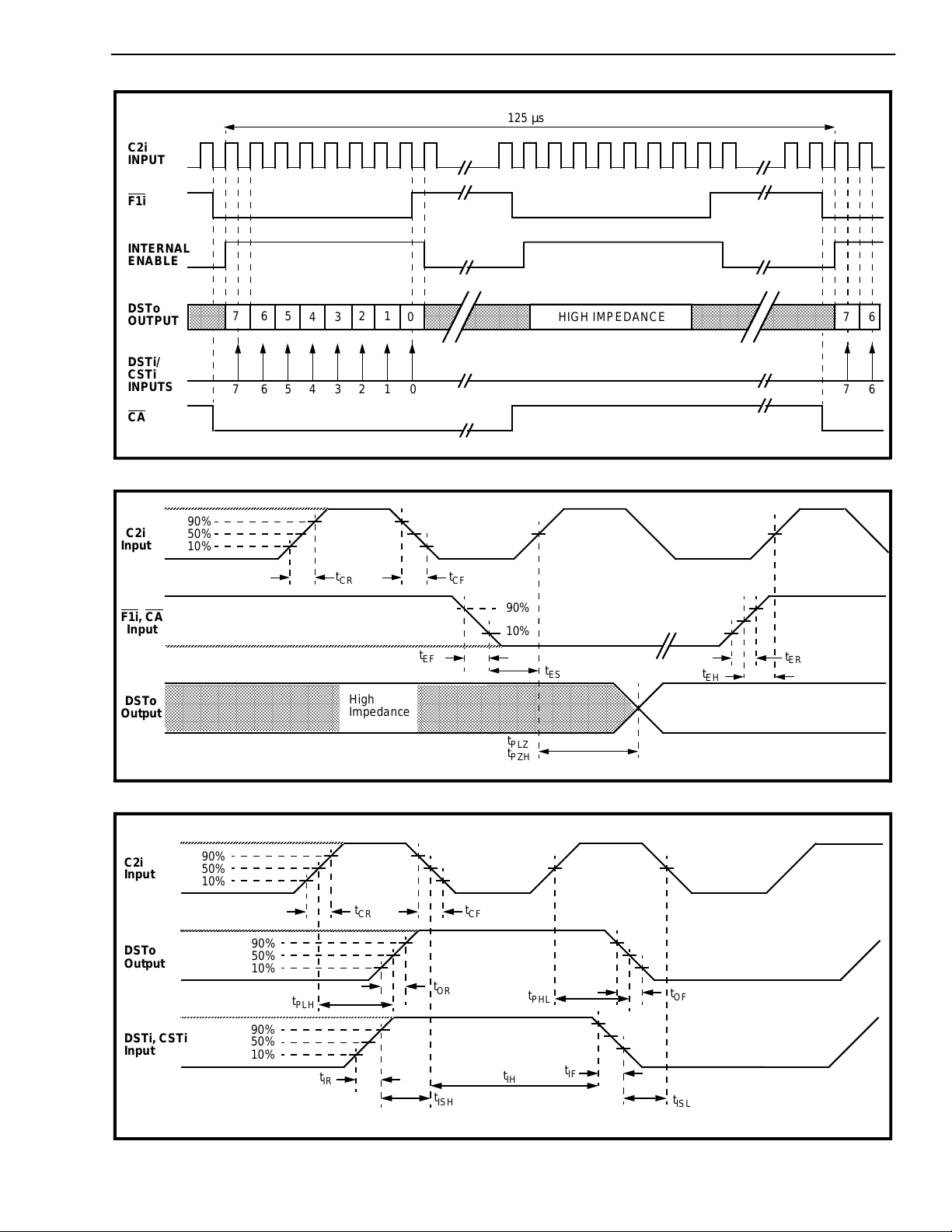
and CSTi) should be enabled for only 8 clock periods
of the C2i clock in any 125µs period (one ST-BUS
frame time) as shown in Figure 11. All data input
and output at the ST-BUS interface takes place at
2.048 Mbps.
MARK
4 µs. Min.
121 µs. Max.
2 on the remote end
X
6-9
Page 8
MT8950 ISO-CMOS
The Secondary Clock input (SCLK) is normally a
600Hz clock signal. This clock is internally aligned
with the 2.048 MHz input. It is used to generate the
synchronizing pulses and the violation word timing
(when the chip is operating in the local carrier mode).
Note that the 600Hz frequency is an exact multiple of
the most commonly used baud rates, i.e., 300, 2400,
4800, 9600, and 19200. In synchronous data
transmission schemes, the receiver timing circuitry
can be kept in sync using the synchronizing pulses
or the violation word when no data is being
transmitted. Other clock f requencies can be used for
specific applications. If this facility is not to be
utilized, the SCLK input can be tied to ground.
Control Interface
An 8 bit word is rea d into th e C o nt rol Reg i ster v ia th e
CSTi input at the same time as the TEM word is
being shif ted in. The chip functions controlled by the
eight bits are summarized in Table 3 and described
in subsequent sections.
Bit Function
7,6,5 Device mode control bits. These bits
select one of eight m odes of operation
4,3,2 Violat ion word control bits
1 Resets the Data Act ivit y Scan point
0 Resets the Uncomm itted S can point
Table 3. Summary of Control Register Function
Modes of Op erati on
As mentioned earlier, the data codec can operate in
eight different modes. The specific mode is selected
through bits 7, 6 and 5 in the Control Register. Table
4 summarizes the different modes.
Mode 0: Normal. This is the normal transparent
conversion mode of the data codec. The NRZ/RZ
input signal is directly encoded into the TEM format
and output as an ST-BUS channel. The TEM word
for the input ST-BUS channel is decoded and the
regenerated data is output via the NRZ/RZ output
circuitry. Synchronizing pulses are also transmitted
as explained in the preceding paragraphs.
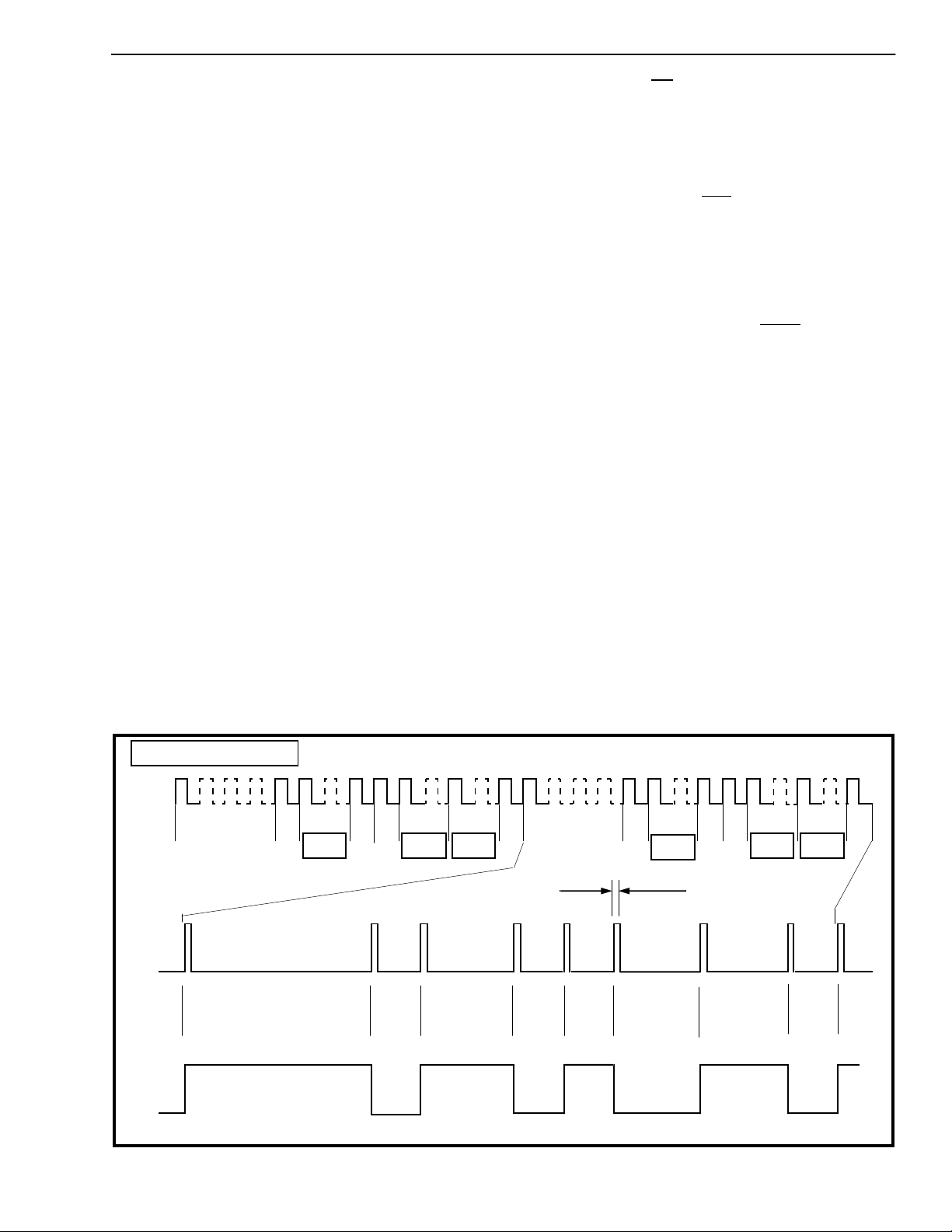
Mode 1: Local Carrier. In this mode the NRZ/RZ
output circuitry transmits an 8 bit word at D
2 (Pin
R
18) by modulating the secondary clock (SCLK). If
the chip has been selected to operate in the RZ
format, this word is transmitted as MARK
Violations. The time interval between consecutive
pulses specifies the binary value. A logical zero is
represented by a time interval of one SCLK period
between the pulses. A logic “1” is represented by
two clock periods. In the NRZ mode, the time
interval between consecutive transitions of the signal
carries the information. The modulation scheme is
illustrated in Figure 6. The 8 bit word consists of a
Control Register
Bits
Mode of Operation
b7 b6 b5
0 0 0 Normal
0 0 1 Local Carrier
0 1 0 Local Synchronization
0 1 1 Digital Loopback
1 0 0 Data Loopback
1 0 1 Data Loopback - Local
Violation Wo rd
1 1 0 Normal Mode - Drive Point
Set HIGH.
111Idle
Tab le 4. M ode s of Op erati on
sync bit followed by seven other bits. Bit s 1, 4 and 5
in this word reflect the values of bits 2, 3 and 4 in t he
Control Register. The remaining four bits in the word
are fixed as zeros. The sync bit is identified by a
time interval equal to four clock periods of SCLK.
The NRZ/RZ input circuitry and the encoder stage
operates normally in this mode.
Mode 2: Local Synchronization. In the local sync
mode, the NRZ/RZ output circuitry transmits only
sync pulses on D
2. These sync pulses appear as
R
MARK violations in the RZ mode with the time
interval between consecutive pulses equal to four
SCLK periods. In the NRZ format D
2 outputs a
R
squarewave with a period equal to eight cycles of
SCLK. D
1 output is held at steady MARK. The
R
NRZ/RZ input circuitry and the enc oder stage of the
chip function norm ally.
Mode 3: Digital Loopback. In this mode an 8 bit
word from the incoming ST-BUS (DSTi) is sampled
and one ST-BUS frame later, the same word is
looped back to the corresponding outgoing channel
of the ST-BUS (DSTo). This allows the user to test
the ST-BUS transmission path to and from the data
codec.
Mode 4: Data Loopback. This mode permits the
user to test the decoding and encoding operation of
the codec. A known TEM word is sent to the data
codec from the ST-BUS end. This word is decoded
and redirected via the output circuitry to the NRZ/RZ
input circuit and subsequently to the encoder stage
6-10
Page 9
ISO-CMOS MT8950
for transmission out on the ST-BUS output pin
(DSTo). The NRZ/RZ inputs (Pins 9 and 10) are
functionally disconnected from the input circuitry.
The outputs (pins 18 and 19) are in a non-active
state, i.e., D
1 is steady LOW and DR2 is steady
R
HIGH.
Mode 5: Data Loopback - Local Violation Word.
This mode can be used for testing the operation of
the chip in the local carrier mode. The Violation word
is generated as in the local carrier mode. However,
the modulated signal is not output on D
2. It is
R
rerouted to the NRZ/RZ input circuit, encoded into
the TEM format and output on DSTo.
Mode 6: Normal Mode - Drive Point Activated.
The drive point output (Pin 14) is set HIGH in this
mode. The codec operation is normal in every other
respect. This drive point can be used to control
external circuitry. It is reset when the mode of
operation is changed.
Mode 7: Idle. In the idle mode DR1 and DR2 outputs
are in a non-active state, i.e., D
and D
2 is steady HIGH. The encoder stage and the
R
1 is steady LOW
R
input circuitry operates normally.
Device Monitoring Features
1. Data Activity (DA
): This output goes from high
to low when a SPACE signal, indicating the
beginning of data activity, is received by the NRZ/
RZ input circuitry. The level on this pin is reset by
setting bit 1 of the Control Register to logic “1”.
2. Scan Point output (SPo
): This output is set
LOW whenever SPi input undergoes a low to high
transition . It is reset by a logic “1” in b it 0 of the
Control Register. The SPi input is generally used
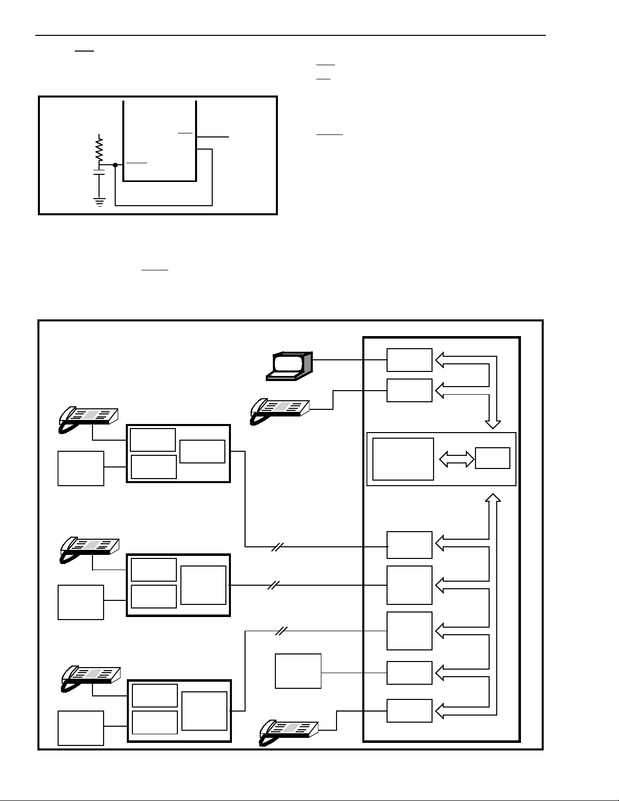
in conjunction with pin 11 to detect a long SPACE
condition in the data. The external circuitry
required to utilize this feature is illustrated in
Figure 7. Note that Pin 11 (NRZo
) is an open
drain output. The NRZ/RZ data input to the
codec is convert ed to the NRZ format and output
on this pin. The RC tim e constant for the circuit
shown in Figure 7 can be set to detect SPACE
conditions of varying time durations. The length
of the long SPACE detected is given by
T
=0.7RC
SP
Where T
is the duration of the SPACE in
SP
milliseconds. A long SPACE of 150ms is
generated when the BREAK key on a data
terminal is depressed. To detect this signal, a
value of R equal to 210 kΩ and C equal to 1.0µF
can be used.
There are two output pins which can be used to
monitor the codec.
CRB = Control Register Bit
SYNCH b0 b1 b2 b3 b4 b5 b6 SYNCH
CRB2 CRB3 CRB4
2
D
R
Output
(RZ
Mode)
D
2
R
Output
(NRZ
Mode)
SYNCH
6.7 ± 0.83 msec
Note: The polarity of this output can be inverted - depending on the state of the last transition.
b0
1.67
msec
b1
0=1.67 msec
1=3.33 msec
CRB2 CRB3 CRB4
Figure 6 - Violation Word Timing in the Local Carrier Mode for a 600Hz input to SCLK
b2
1.67
msec
b3
1.67
msec
b0 b1 b2 b3 b4 b5 b6
CRB2 CRB3 CRB4
35 µs Nominal
b4
0=1.6 7 ms ec
1=3.3 3 ms ec
b5
0=1.67 msec
1=3.33 msec
b6
1.67
msec
SYNCH
6-11
Page 10
MT8950 ISO-CMOS
The SPo pin could then be monitored by the
system processor to detect a prompt from the
peripheral.
MT8950
R
C
+5V
11
NRZo
SPo
SPi
16
15
Figure 7 - Long Space Detection Circuit
External P owe r Reset
When the reset input (PRST) is taken low, the data
codec circuit goes into reset mode. The conditions
present on the output pins are as follows:
Data Terminal
Equipment
1. DSTo - High Impedance
2. SPo
3. DA
- +5V (unasserted)
- +5V (unasserted)
4. DP - GND (unasserted)
1-+5V(inactive)
5. D
R
6. D
2-GND(inactive)
R
7. NRZo
- GND (Mark condition)
The internal Control Register is loaded with HEX
FF.
Applications
A block diagram schematic of a simple Voice-Data
integrated switching system is illustrated in Figure 8.
The data terminal can access a number of remote
devices via the gateway provided by the Data
Codec. In this application, the Data Codec function
parallels that of the Voice Codec, i.e., the Voice
Digital PBX
Data
Codec
Main
Frame
Computer
Main
Frame
Computer
Main
Frame
Computer
Voice
Codecs
Data
Codecs
Voice
Codecs
Data
Codecs
Voice
Codec
Data
Codec
T1/CEPT
Interface
Digital
Line
Interface
Digital
Network
Interface
T1/CEPT Leased Lines
1.544 Mbit/s or 2.048 Mbit/s
256 kbit/s
Digital Line
160/80
kbit/s
Main
Frame
Computer
Voice
Codec
ST-BUS Format
MT8980
Digital Switch
T1/CEPT
Interface
Digital
Line
Interface
Digital
Network
Interface
Data
Codec
Voice
Codec
MPU
ST-BUS Format
6-12
Figure 8 - Voice-Data integration using the Data Codec
Page 11
ISO-CMOS MT8950
AAAA
AAAA
AAAA
AAAA
AAAA
AAA
AAAA
AAAA
A
A
A
A
A
A
A
A
AAAA
AAAA
AAAA
A
Codec converts analog signals into the ST-BUS
format while the Data Codec does a similar
conversion for low speed data. The information in
the ST-BUS format can be switched via the Digital
Switch to any of the other interfaces and
subsequently transm itted over the appropriate lines
to the remote destination. At the rem ote end, the
original signal is regenerated by another codec.
The remote equipment can be part of a local area
network or it may be accessed through leased T1/
CEPT digital lines. Access to remote equipment via
the T1/CEPT leased lines is acquired throu gh the T1/
CEPT interface (MT8976). Full duplex transmission
at 1.544 or 2.048 Mbps is possible with this interface.
The Digital Network Interface Circuit (DNIC), the
MT8972, is capable of providing 160 kbps full duplex
transmission over single telephone pair wiring. This
device can support two 64 kbps channels, allowing
two data cod ecs to be interface d to it at the remote
end. Simple, low cost data sets can be construct ed
using the data codec and the DNIC.
A simplified interface for transmitting and receiving
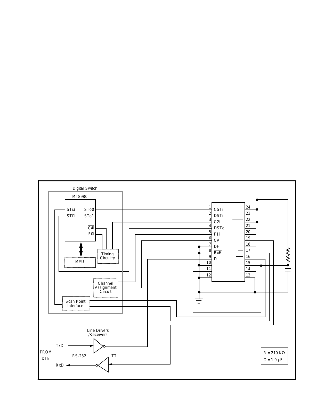
RS-232 data signals is illustrated in Figure 9. The
Codec is selected to receive and transmit low speed
data in the N RZ fo rmat . The da ta tran smitte d by th e
terminal equipment in the RS-232 format is inverted
and level shifted to TTL-compatible levels before
being fed into the D
1 input on the Codec. The
X
signal is converted into the ST-BUS format and
transmitted via the DSTo output in one channel
timeslot when the ST-BUS interface is enabled by
and CA, as dictated by the system channel
F1i
assignment scheme. During this same time period
the Codec accepts the 8 bit data arriving on the
incoming ST-BUS stream which is output at the STo1
pin on the MT8980. The data is decoded and the
original signal input at the remote end is regenerated
and output at the D
1 pin. This signal is level
R
shifted, inverted and transmitted to the terminal. The
codec in this particular application requires no other
programming. Loading of the Control Register via
the CSTi input is optional. If this input is tied to
ground, the Codec will operate in mode 0 (the normal
mode). Note that the SCLK input is tied low. Thus
synchronization pulses will not be transmitted and
Digital Switch
MT8980
STi3
STi1
MPU
Scan Point
Interface
STo0
STo1
C4i
F0i
Channel
Assignment
Line Drivers
/Receivers
Timing
Circuitry
Circuit
10
11
12
1
2
3
4
5
6
7
8
9
CSTi
DSTi
C2i
DSTo
F1i
CA
DF
RxE
DX1
D
2
X
NRZo
V
SS
MT8950
PRST
SCLK
V
DD
NC
NC
NC
DR1
D
R
DA
SPo
SPi
DP
+ 5V
24
23
22
21
20
19
18
2
17
16
R
15
14
C
13
TxD
FROM
DTE
RS-232 TTL
R = 210 KΩ
C = 1.0 µF
RxD
Figure 9 - Simplified RS-232 Interface using the Data Codec
6-13
Page 12
MT8950 ISO-CMOS
A
AAAA
AAAA
AAAA
AAAA
AAAA
AAAA
AAAA
AAAA
AAAA
AAAA
AAAA
AAAA
AAAA
AAAA
AAAA
AAAA
AAAA
AAAA
AAAA
AAAA
AAAA
AAAA
AAAA
AAAA
AAAA
AAAA
AAAA
AAAA
AAAA
AAAA
AAA
RTS
CTS
DSR
DTR
RLSD
TxD
RxD
Level
Converters
Random Logic
or
Microcomputer
NRZ /
Bipolar
Converter
Line
Driver /
Receiver
Bipolar RZ signal
DTE RS-232 TTL
Receiver
D
Bipolar to
Unipolar
Converter
2
X
D
1
X
DSTo
D
Unipolar
to Bipolar
Converter
2
R
D
1
R
Line Driver
Bipolar RZ signal
DSTi
Line
Driver /
Receiver
Digital PBX
STo1
STi1
MPU
NRZ /
Bipolar
Converter
STo3
STi3
Random Logic
Microcomputer
DSTi
MT8950MT8980MT8950
D
2
X
D
1
X
Receiver
Bipolar to
Unipolar
Converter
DSTo
2
D
R
D
1
R
Unipolar
to Bipolar
Converter
Line Driver
DTERS-232TTL
RTS
CTS
or
Level
Converters
DSR
DTR
RLSD
TxD
RxD
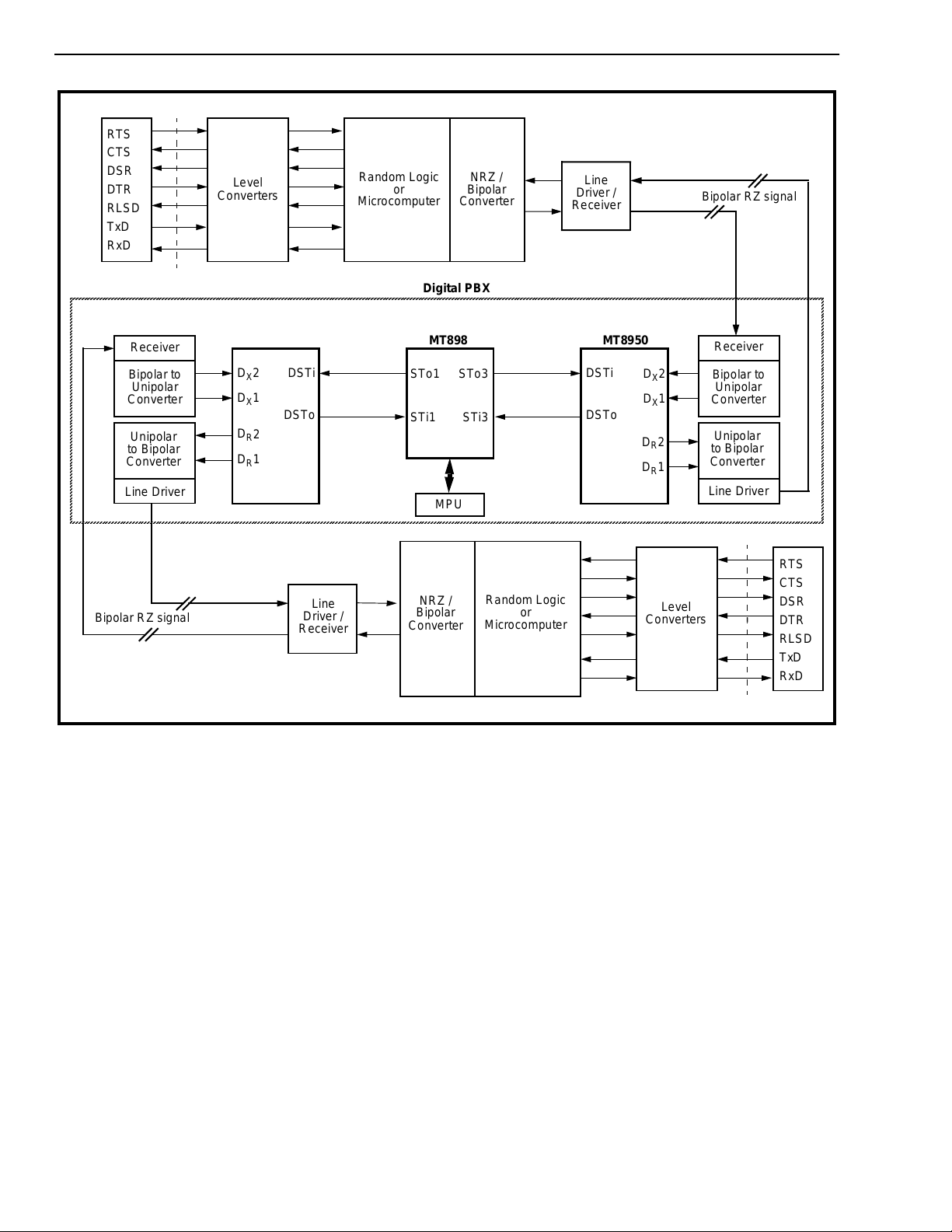
Figure 10 - Block Diagram Illustration of a Scheme to Submultiplex RS-232 Control Signals
the codec cannot be used in the local carrier mode.
If this facility is to be used, an appropriate clock can
be input to the device. The long SPACE detection
circuitry and the Data Ac ti vity outpu t can be used fo r
monitoring the codec if necessary.
Figure 10 shows a block diagram schematic of a
circuit which could be used to submultiplex RS-232
control signals with the data. The data and control
signals are operated on by the microprocessor or the
logic circuitry and subsequently transmitted as a
three level signal. The control signals are encoded
as bipolar violations. Since the control status does
not change very frequently during a call, this
information is transmitted only when no data is
available. Circuitry near the Codec converts the
bipolar signal into a unipolar format and inputs it at
D
1 and DX2. Conversely, the low speed data from
X
the Codec output at D
1 and DR2 is first converted
R
to the bipolar format before being transmitted.The
Data Codec is selected to operate in the RZ format.
The microprocessor or the random logic circuit
examines the received signal for violations. If a
stream of violations is detected, then the signal is
interpreted to be control information. The detected
violations are decoded and the appropriate change
in the status of the RS-232 control signals is
implemented. If no violations are detected then the
incoming signal is considered to be the data and it is
rerouted to the RxD pin of the RS-232 connector.
The microprocessor c ould also be used in the initial
call setup and for error checking of the received
control information. This scheme could be used to
provide transparent modem capability to any of the
ST-BUS based equipment.
6-14
Page 13
ISO-CMOS MT8950
Absolute Maximum Ratings*- Voltages are with respect to ground (V
) unless otherwise stated.
SS
Parameter Symbol Min Max Units
1 Supply Voltage V
2 DC Input Voltage V
3 DC Output Voltage V
4 Input Diode Current ( V
5 Output Diode Current ( V
<0 or VI>VDD)IIK± 10 mA
I
<0 or VO>VDD )I
O
6 DC Output Current, per pin I
7 DC Supply or Ground Current I
8 StorageTemperature T
9 Package Power Dissipation (CERDIP ) T
* Exceeding these values ma y cause perm anen t dama ge. Functi onal operati on und er these cond ition s is not implied.
= 25o CP
A
DD
IN
OUT
OK
O
DD/ISS
ST
D
Recommended Operating Conditions - Voltages are with respect to ground (V
Characteristics Sym Min Typ
1 Supply Voltage V
2 Operating Frequency f
3 Operating Temperature T
‡ Ty p ical figures are at 25°C and are for design aid only: not guarante ed and not subject to producti on testing.
DD
CK
A
4.5 5.0 5.5 V
070
‡
Max Uni ts Test Conditions
2.048 MHz
-0.5 7.0 V
VSS-0.3 VDD+0.3 V
VSS-0.3 VDD+0.3 V
-65 150
) unless otherwise stated.
SS
o
C
± 20 mA
± 25 mA
± 50 mA
o
C
1.0 W
DC Electrical Characteristics
VDD=5.0V±10%; VSS=0V; TA=0oC to 70oC - Voltages are with respect to ground (VSS) unless otherwise stated.
Characteristi cs Sym Min Typ‡Max Units Test Condi tio ns
1
2 Operating supply current I
Quiescent Supply Current I
S
QS
DD
U
P
3
TTL inputs
4 CMOS inputs
I
N
P
5 CMOS Sch mi tt input s
U
T
S
6 SPi Compara tor ON Voltage V
7 SPi Compara tor OF F Voltage V
8 Input Leakage Current I
‡ Ty p ical figures are at 25°C and are for design aid only: not guarante ed and not subject to producti on testing.
1. Includ e D S Ti, C STi, C 2i , F1i
2. Includ e D F
3. Includ e RxE
,DX1, DX2 and PRST
1
HIGH voltage
LOW voltage
2
HIGH voltage
LOW voltage
HIGH voltage
LOW voltage
and SCLK
V
V
V
V
3
V
V
T+
IN
2.0
IH
V
IL
IH
IL
IH
IL
3.5
V
3.0
V
SS
SS
SS
2.25 2.5 2.75 V VDD = 5V
2.0 V VDD = 5V
T-
±1 ±10 µA VDD = 5V
150 µA All outputs unloaded
All inputs @ V
1.0 mA All outputs unloaded.
Input pins 2 and 3 clocked
at 2.048 MHz.
Pins 1,8,15,20,21 @ V
Pins 5,6,7,9,10,13 and 22
@V
V
0.8
V
1.5
V
1.0
DD
DD
DD
V
V
V
V
V
V
SS
SS
DD
6-15
Page 14
MT8950 ISO-CMOS
DC Electrical Characteristics
VDD=5.0V±10%; VSS=0V; TA=0oC to 70oC - Voltages are with respect to ground (VSS) unless otherwise stated.
Characteristics Sym Min T yp‡Max Un its Test Cond i tion s
1
Output LOW volta ge V
2 Outpu t HIGH Voltage V
3 Outpu t LOW Current (On all
O
outputs except DSTo)
U
4 Outpu t HIGH Curre nt (On all
T
outputs except DSTo)
P
U
5 Outpu t LOW Current (On
T
DSTo output )
S
6 Outpu t HIGH Current (On
I
I
I
I
OL
4.95 V | IO |< 1.0 µA VDD = 5V
OH
OL
OH
OL
OH
2.2 2.8 mA VOL=0.4V
-3.5 -4.2 mA VOH=2.4V
8.9 11.1 mA VOL=0.4V
-14.0 -16.8 m A VOH=2.4V
0.05 V | IO |< 1.0 µA VDD = 5V
DSTo output )
7 Output Leakage Current I
‡ Ty p ical figures are at 25°C and are for design aid only: not guaranteed and not subject to producti on testing.
†
AC Electrical Characteristics
- Voltages are with respect to ground (V
OZ
Characteristics Sym Min Typ
1 C2i Clock Frequency f
2 C2i Clock Rise Time t
3 C2i Clock Fall Time t
CK
CR
CF
±1 ±10 µA
) unless otherwise stated.
SS
‡
Max Units Test Condition s
2.028 2.048 2.068 MHz
50 ns
50 ns
4 Clock Duty Cycle (C2i & SCLK) 50 %
5 SCLK Clock Frequency f
6 SCLK Clock Rise Time t
7 SCLK Clock Fall Time t
8F1i
9F1i
10 F1i
11 F1i
and CA Rise Time t
and CA Fall Time t
and CA Setup Time t
and CA Hold Time t
12 DSTo Rise Time t
13 DSTo Fall Time t
14 Propagation Delay From Clock
(C2i) To O utput (DSTo) enable.
15 Propagation Delay From Clock
(C2i) To Output (DSTo).
16 Input Rise Time (DSTi, CSTi) t
17 Input Fall Time (DSTi, CSTi ) t
18
DSTi, CSTi Setup Time
19 DSTi, CSTi Hold Tim e t
20 PRST
† Timing is over recommended temperature & power supply voltages.
‡ Ty p ical figures are at 25°C and are for design aid only: not guaranteed and not subject to producti on testing.
Note 1:
R
=10KΩ to VDD, CL=150 pF to V
L
Low Time 488 ns
SS
SCLK
SCLKR
SCLKF
ER
EF
ES
EH
OR
OF
t
PZH
t
PZL
t
PLH
t
PHL
IR
IF
t
ISH
t
ISL
IH
00.6128kHz
50 ns
50 ns
100 ns
100 ns
25 ns
-25 25 ns
100 ns Note 1
100 ns Note 1
125 ns Note 1
125 ns Note 1
100 ns
100 ns
0ns
90 ns
6-16
Page 15
AAAA
AAAA
AAAA
AAAA
AAAA
AAAA
AAAA
AAAA
AAAA
AAAA
AAAA
AAAA
AAAA
AAAA
AAAA
AAAA
AAAA
AAAA
AAAA
AAAA
AAAA
AAAA
AAAA
AAAA
AAAA
AA
AA
AA
AA
AA
AAAA
AAAA
AAAA
AAAA
AAAA
AAAA
AAAA
AAAA
AAAA
AAAA
A
A
A
A
A
AAAA
AAAA
AAAA
AAAA
AAAA
C2i
AAAA
AAAA
AAAA
AAAA
AAAA
AAAA
A
A
A
A
A
A
A
AA
AAAA
AAAA
AAAA
AAAA
AAAA
AAAA
AAAA
AAAA
AAAA
AAAA
AAAA
AAAA
AAAA
AAAA
AAAA
AAAA
AAAA
AAAA
AAAA
AAAA
AAAA
AAAA
AAAA
AAAA
AAAA
AAAA
AAAA
AAAA
AAAA
AAAA
AAAA
AAAA
AAAA
AAAA
AAAA
AAAA
AAAA
AAAA
AAAA
AAAA
AAAA
AAAA
AAAA
AAAA
AAAA
AAAA
AAAA
AAAA
AAAA
AAAA
AAAA
AAAA
AAAA
AAAA
AAAA
AAAA
AAAA
AAAA
AAAA
AAAA
AAAA
AAAA
AAAA
AAAA
AA
AA
AA
AA
AA
AA
AA
AA
AAAA
AAAA
AAAA
AAAA
AAAA
AAAA
AAAA
AAAA
AAAA
A
INPUT
F1i
INTERNAL
ENABLE
ISO-CMOS MT8950
125 µs
DSTo
OUTPUT
DSTi/
CSTi
INPUTS
CA
C2i
Input
, CA
F1i
Input
DSTo
Output
AAAA
AAAA
AAAA
AAAA
AAAA
AAAA
AAAA
90%
50%
10%
AAAA
AAAA
AAAA
AAAA
AAAA
AAAA
AAAA
AAAA
AAAA
AAAA
AAAA
AAAA
AAAA
AAAA
AAAA
AAAA
AAAA
AAAA
AAAA
AAAA
AAAA
AAAA
AAAA
AAAA
AAAA
AAAA
AAAA
AAAA
567
34
12
0
01234567 67
Figur e 11 - Timi ng Di ag ram - 12 5 µs Frame Period
t
CF
90%
10%
t
EF
t
ES t
t
PLZ
t
PZH
AAAA
AAAA
AAAA
AAAA
AAAA
AAAA
AAAA
AAAA
AAAA
AAAA
AAAA
AAAA
AAAA
AAAA
t
CR
A
A
High
A
A
Impedance
A
A
A
EH
67HIGH IMPEDANCE
t
ER
C2i
Input
DSTo
Output
DSTi, CSTi
Input
90%
50%
10%
Figure 12 - Timing Diagram - ST-BUS Interface Enable
90%
50%
10%
90%
50%
10%
t
PLH
t
CR
t
IR
t
CF
t
t
OR
ISH
t
PHL
t
t
IH
IF
t
OF
t
ISL
Figure 13 - Timing Diagram - ST-BUS Input/Output
6-17
Page 16

MT8950 ISO-CMOS
NOTE S:
6-18
 Loading...