

Page 1
9-127
Features
• Operates from single or dual power supply
• MH89726 extends transmission performance
for the MT8972 (DNIC) at 160kbit/s line rate
• MH89728 extends transmission performance
for the MT8972 (DNIC) at 80kbit/s line rate
• MH89726 and MH89728 are pin for pin
compatible with each other
• Compact SIL package
• Over 6km loop range on 24 AWG
Applications
• Digital subscriber lines
• Digital PABX line cards and telephone sets
• High speed, limited distance modem
• ISDN U - Interface
Description
The MH89728 and MH89726 are thick film hybrid
devices which may be used to extend the operating
range of the MT8972 (DNIC). The hybrids combine
signal equalization and amplification for the receive
and transmit paths on each device.
The small size of these hybrids makes them suitable
for line card or terminal use with the MT8972. The
gain of the t ransmit signal ma y be adjusted th rough
the use of a n ex te rn al r e sis t or.
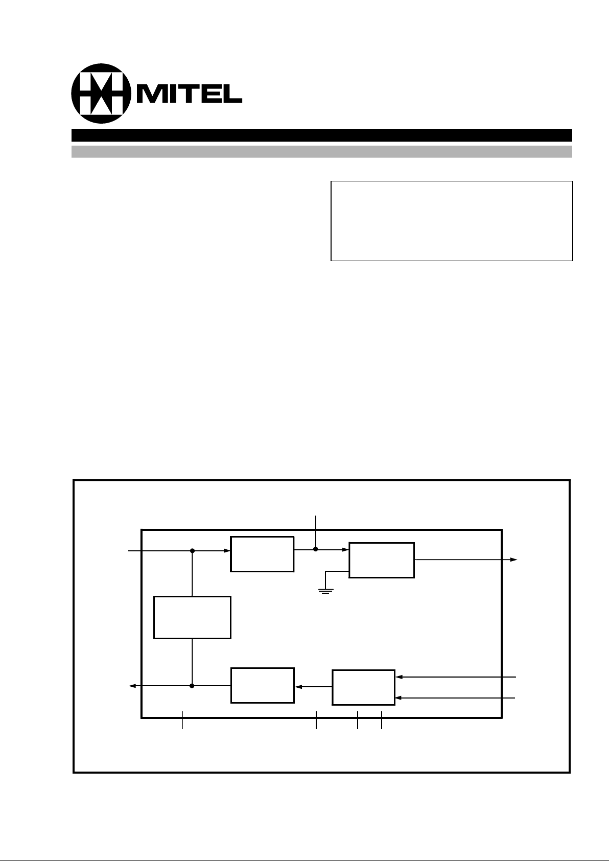
Figure 1 - Functional Bloc k Diagram
TX
IN
RX
OUT
V
Bias
TEST V+V
-
RX
IN
-
RX
IN
+
TX
OUT
TX
GAIN
Pre-
Equalizer
Phase
Compensator
Pre-
Canceller
RX
Amplifier
TX
Amplifier
Ordering Information
MH89726/728 10 Pin SIL Package
0°C to 70°C
ISSUE 2 November 1990
MH89726/728
MT8972 Loop Extender Circuits
Advance In formation
Page 2
9-128
MH89726/728 Advance Information
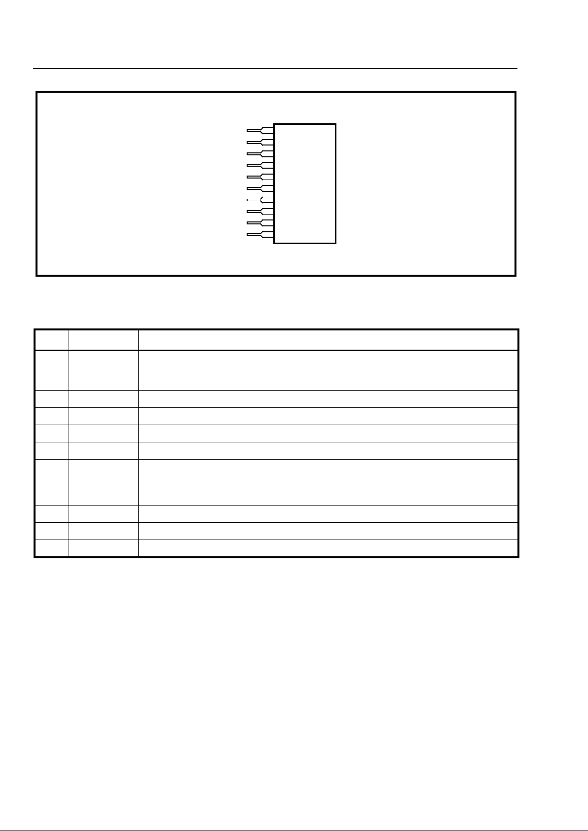
Figure 2 - Pin Conn ections
Pin Description
Pin # Pin Name Description
1TX
GAIN
Transmit Gain. To be connected to Pin 2. An increase in gain can be achieved by
connecting an external resistor R
EXT
between Pin 1 and Pin 2. The resultant gain is
calculated using; A= (R/24) + 2.8, where A=Gain and R= R
EXT
(kΩ).
2TX
OUT
Transmit Output. Connect to the termination network.
3RX
IN-
Negative Receive Signal. Connect to TX
OUT
, Pin 2.
4RX
IN+
Positive Receive Signal. Connected to line transformer.
5V-Negative power supply.
6V
Bias
Internal Bias Voltage. Connect to GND through 0.33 µF for single power supplies.
Connect to GND directly for split power supplies.
7V+Positive power supply.
8TESTTest. Used for production testing. Leave unconnected.
9RX
OUT
Receive Output. Connect to LIN (Pin 21) of MT8972.
10 TX
IN
Transmit Input. Connect to L
OUT
(Pin 1) of MT8972.
1
2
3
4
5
6
7
8
9
10
TXGAIN
TXOUT
RXIN +
RXIN -
V -
VBias
V +
TEST
RXOUT
TXIN
Page 3

9-129
Advance Information MH89726/728
Functional Description
The MH89726/728 are 10 pin SIL thick film hybrid
circuits that may be used to extend the loop range
capability of the MT8972 (DNIC). For a detailed
description of the DNIC, refer to the MT8972 data
sheet.
Figure 1 shows a block diagram of the Loop
Extender Circuit (LEC). The LEC takes the line
signal which is transmitted by the DNIC on L
OUT
, preequalizes, and amplifies it before sending it to the
termination network. The gain of the TX amplifier is
adjustable by using an external resistor between
pins 1 and 2. If no external resistor is added, TX
GAIN
and TX
OUT
must be shorted tog e th er, and the defaul t
gain condition exists. This gain results in a transmit
signal power level of +10 dBm.
On the receive side, the LEC receives the differential
line signal from the transformer, and performs firstorder pre-cancellation as well as gain and phase
adjustment of the receive signal. The signal is then
output on RX
OUT
which is connected to LIN of the
MT8972.
Tables 1 and 2 show typical results obtained by
using the LEC with the MT8972. Actual distance
achieved may vary depending on the characteristics
of the transmission cable being used. Most
important factors include cable attenuation (dB/km),
bridged taps, an d cros stal k int erfer enc e.
The LEC is powered typically from ±15 Volts if dual
power supplies are available. Alternately 0 to +30
Volts, or -30 to 0 Volts can be u sed if only a single
power supply is available.
Applications
Figure 3 show s a typical connectio n diagram of the
MT8972 and MH 8972 6/72 8. R X
OUT
and T
XIN
of the
LEC are connected to L
OUT
and LIN of the DNIC
respectively. Pins 5, 6 and 7 are the power supply
pins, with the voltages being supplied as indicated in
the table . An external resistor, R
EXT
, may be use d
to increase the ga i n of the transm i tt er. Without R
EXT
,
TX
GAIN
and TX
OUT
are shorted toge ther resulting i n
a transmit power level of +10 dBm.
R
LL
, RL, and CL comprise the termination network
and are used to match the characteristic impedance
of the transmiss ion lin e. T his pr o vide s th e 4 wi r e t o 2
wire hybrid conversion necessary for twisted pair
transmission.
Figure 4 shows a typical application of the LEC. On
short loops, jumpers (or switches) could be used to
remove the LEC from the circuit. For longer loops,
the jumpers could be changed to include the LEC in
the signal path.
Figure 3 - Typical Connection Diagram for MT8972 and MH89726/728
MT8972
(DNIC)
MH89726
or
MH89728
+ 5V
22
1
21
11
D1
D2
10987654321
To Power Supplies
R
ext
R
LL
RLC
L
0.33µF
1.0µF
100kΩ
D1, D2 IN5817
R
ext
Set for different gain requirements
MH89726
160 kbit/s
MH89728
80 kbit/s
R
LL
R
L
C
L
3.9kΩ, 5%
430Ω, 2%
15nF, 5%
3kΩ, 5%
430Ω, 2%
12nF, 5%
Power
Supply
DUAL
SINGLE
SINGLE
Pin 7
(V +)
+ 15V
GND
+ 30V
Pin 6
(V
Bias
)
GND
GND*
GND*
Pin 5
(V-)
- 15V
- 30V
GND
*Use 0.33µF capacitor to GND
Page 4

9-130
MH89726/728 Advance Information
Table 1 - Typical Transmission Performance at 160 kbit/s
Table 2 - Typical Transmission Performance at 80 kbit/s
Note 1: The attenuation of the cable as specified by Bell System Technical Reference PUB 62411.
Figure 4 - Typical Application of th e L oop E xten der
MH89726 (160 kbit/s)
CABLE
CONFIGURATION
24 AWG
(8.0 dB/km at 120 kHz)
26 AWG
(11.5 dB/km at 120 kHz)
DNIC to DNIC 0.0 to 4.1 km 0.0 to 3.0 km
DNIC with LEC to DNIC with LEC 0.65 to 5.1 km 0.5 to 3.6 km
MH89728 (80 kbit/s)
CABLE
CONFIGURATION
24 AWG
(6.9 dB/km at 60 kHz (Note 1)
26 AWG
(10.0 dB/km at 60 kHz)
DNIC to DNIC 0.0 to 5.2 km 0.0 to 3.4 km
DNIC with LEC to DNIC and LEC 0.9 to 6.5 km 0.65 to 4.1 km
L
OUT
L
IN
1
+5V
21
D1
D2
LE
IN
LE
OUT1
CA
CB
RA
LOOP
EXTENDER
and
Network
Termination
MT8972
LE
OUT2
0.33µF
1.0µF
2:1
Twisted Pair
Copper 24-26
Gauge
NOTES:
-D1, D2 IN5817 (Schottky)
-Solid jumpers used to connect the loop extender
-Dotted jumpers connect MT8972 without loop extender
80 kbit/s RA = 390Ω CA = 22nF CB = 3.3nF
160 kbit/s RA = 390Ω CA = 22nF CB = 1.5nF
Page 5

9-131
Advance Information MH89726/728
Note 1: A single voltage supply of +30V±10% can be used on VDD with V
Bias
grounded through a 0.33 µF capacitor and VSS
grounded.
Note 2: A single voltage supply of -30V±10% can be used on VSS with V
Bias
grounded through a 0.33 µF capacitor and VDD
grounded.
Recommended Operating Conditions
Characteristics Sym Min Typ Max Units Test Conditions
1 + 15 V Supply V
DD
13.5 15.0 16.5 V Note 1
2 - 15 V Supply V
SS
-16.5 -15.0 -13.5 V Note 2
3 Standby Current I
S
3.0 mA
A.C. Electrical Characteristics
Characteristics Sym Min Typ Max Units Test Conditions
1 Active Current I
A
7.0 mA @ 60 kHz for 80 kbit/s
@120 kHz for 160 kbit/s
2TX Gain A
TX
9.0 dB @ 60 kHz for 80 kbit/s
@120 kHz for160 kbit/s
3 TX Phase Angle Φ
TX
-170.0 ° @ 60 kHz for 80 kbit/s
@120 kHz for 160 kbit/s
4 RX Gain A
RX
0.0 dB @ 60 kHz for 80 kbit/s
@120 kHz for160 kbit/s
5 RX Phase Angle Φ
RX
12.0 ° @ 60 kHz for 80 kbit/s
@120 kHz for160 kbit/s
6 Line Power 10.0 dBm With 2:1 transformer
Page 6

9-132
MH89726/728 Advance Information
Figure 4 - Mechanical Data
0.405 -
0.345
(1.029 -0.876)
0.105 - 0.095
(0.241 - 0.267)
0.025 - 0.015
(0.064 - 0.038)
0.190 - 0.180
(0.483 - 0.457)
All dimensions are in inches (centimeters).
0.140 (0.356)
1.020 - 0.980 (2.590 - 2.490)
0.01 (0.025)
 Loading...