

Page 1
Cascadable Silicon Bipolar
MMIC␣ Amplifier
Technical Data
MSA-0504
Features
• Cascadable 50 Ω Gain Block
• High Output Power:
18.0 dBm Typical P
1.0␣ GHz
1 dB
at
in a low cost plastic package. This
MMIC is designed for use as a
general purpose 50 Ω gain block.
Typical applications include
narrow and broad band IF and RF
amplifiers in commercial systems.
• Low Distortion:
29.0 dBm Typical IP3 at 1.0␣ GHz
• 7.0 dB Typical Gain at
1.0␣ GHz
• Low Cost Plastic Package
The MSA-series is fabricated using
HP’s 10 GHz fT, 25␣ GHz f
silicon bipolar MMIC process
which uses nitride self-alignment,
ion implantation, and gold metallization to achieve excellent
Description
The MSA-0504 is a high performance medium power silicon
bipolar Monolithic Microwave
Integrated Circuit (MMIC) housed
performance, uniformity and
reliability. The use of an external
bias resistor for temperature and
current stability also allows bias
flexibility.
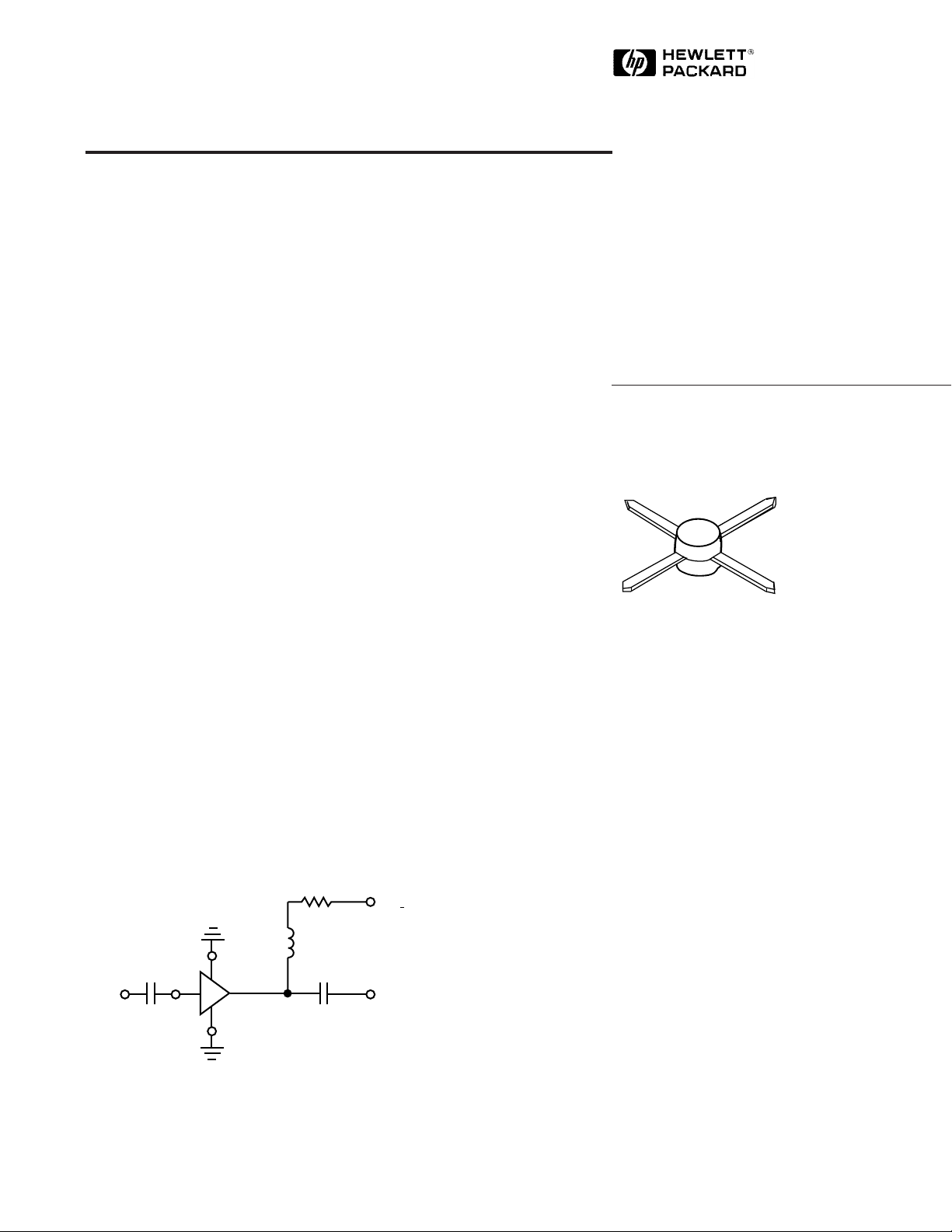
Typical Biasing Configuration
R
bias
04A Plastic Package
,
MAX
V
> 12 V
CC
RFC (Optional)
C
block
IN OUT
4
3
MSA
1
2
V
= 8.4 V
d
C
block
5965-9580E
6-350
Page 2
MSA-0504 Absolute Maximum Ratings
Parameter Absolute Maximum
Device Current 135 mA
Power Dissipation
[2,3]
1.5 W
RF Input Power +25 dBm
Junction Temperature 200°C
Storage Temperature –65 to 150° C
[1]
Thermal Resistance
θjc = 75°C/W
Notes:
1. Permanent damage may occur if
any of these limits are exceeded.
2. T
3. Derate at 13.3 mW/° C for T
CASE
= 25°C.
4. See MEASUREMENTS section
“Thermal Resistance” for more
Electrical Specifications
[1]
, T
A
= 25° C
Symbol Parameters and Test Conditions: Id = 80 mA, Z
P
1 dB
Output Power at 1 dB Gain Compression f = 0.5 GHz dBm 19.0
= 50 Ω Units Min. Typ. Max.
O
information.
f = 1.0 GHz dBm 16.0 18.0
G
P
Power Gain (|S21|2) f = 0.5 GHz dB 7.5
f = 1.0 GHz 6.0 7.0
∆G
f
3 dB
VSWR
IP
3
Gain Flatness f = 0.1 to 1.5 GHz dB ±0.75
P
3 dB Bandwidth
[2]
GHz 2.3
Input VSWR f = 0.1 to 1.5 GHz 1.6:1
Output VSWR f = 0.1 to 1.5 GHz 2.0:1
Third Order Intercept Point f = 1.0 GHz dBm 29.0
NF 50 Ω Noise Figure f = 1.0 GHz dB 6.5
t
D
V
d
Group Delay f = 1.0 GHz psec 180
Device Voltage V 6.7 8.4 10.1
dV/dT Device Voltage Temperature Coefficient mV/°C –16.0
Notes:
1. The recommended operating current range for this device is 60 to 100 mA. Typical performance as a function of current
is on the following page.
2. Referenced from 0.1 GHz Gain (G
).
P
[2,4]
:
> 88°C.
C
6-351
Page 3

MSA-0504 Typical Scattering Parameters (T
0
2
4
6
8
10
81012141618202224
POWER OUT (dBm)
Figure 1. Typical Gain vs. Power Out,
T
A
= 25°C, Id = 80 mA.
0.1 GHz
0.5 GHz
1.0 GHz
1.5 GHz
2.0 GHz
GAIN (dB)
VSWR
FREQUENCY (GHz)
FREQUENCY (GHz)
Figure 2. VSWR vs. Frequency,
I
d
= 80 mA.
1:1
2:1
3:1
4:1
5:1
6:1
4.0
0.1 0.2 0.3 0.5 2.01.0
Output
Input
Figure 3. Device Current vs. Voltage.
30
60
90
120
Id (mA)
V
d
(V)
0
036912
T
C
= +85°C
T
C
= +25°C
T
C
= –25°C
12
14
18
16
22
20
P
1 dB
(dBm)
TEMPERATURE (°C)
Figure 4. Output Power at 1 dB Gain
Compression, vs. Case Temperature,
I
d
= 80 mA.
18
26
22
30
–25 0 +25 +85
14
34
P
1 dB
(dBm)
I
d
(mA)
Figure 6. Output Power at 1 dB Gain
Compression, Third Order Intercept
vs. Current, f = 1.0 GHz.
Figure 5. Gain vs. Frequency,
I
d
= 80 to 100 mA.
60 70 80 90 100
IP
3
(dBm)
0.5 GHz
1.0 GHz
2.0 GHz
.01 .05 0.1 0.5 1.0 5.0
14
12
10
8
6
4
2
0
Gp (dB)
IP
3
P
1 dB
Freq.
S
11
S
21
= 25° C, I
A
S
= 80 mA)
d
12
S
22
MHz Mag Ang dB Mag Ang dB Mag Ang Mag Ang k
5 .54 –43 14.7 5.43 160 –18.4 .120 37 .63 –39 0.60
25 .24 –112 9.3 2.92 155 –13.8 .204 12 .24 –101 0.99
50 .18 –142 8.1 2.54 161 –13.7 .206 3 .16 –125 1.17
100 .14 –156 7.8 2.45 166 –13.7 .207 3 .13 –137 1.18
200 .14 –168 7.6 2.40 163 –13.7 .206 1 .13 –146 1.20
400 .14 –174 7.5 2.37 150 –13.7 .206 1 .16 –143 1.19
600 .14 –175 7.4 2.34 137 –13.6 .208 –1 .20 –144 1.18
800 .15 –174 7.2 2.29 124 –13.5 .211 –1 .25 –148 1.15
1000 .17 –174 7.0 2.24 111 –13.6 .209 –3 .29 –154 1.14
1500 .23 –179 6.4 2.09 80 –13.3 .216 –4 .37 –168 1.06
2000 .33 171 5.5 1.88 51 –12.8 .230 –10 .48 178 0.91
2500 .42 156 4.3 1.64 27 –13.0 .224 –12 .51 165 0.90
3000 .49 146 3.2 1.44 6 –12.8 .230 –11 .55 157 0.92
A model for this device is available in the DEVICE MODELS section.
Typical Performance, T
(unless otherwise noted)
= 25° C
A
6-352
Page 4

04A Plastic Package Dimensions
)
12.39 ± 0.76
(0.488 ± 0.030)
4
GROUND
RF INPUT
0.76 (0.030)
2.54 ± 0.25
(0.100 ± 0.010)
1
4.29
(0.169)
0.51
(0.020)
DIMENSIONS ARE IN MILLIMETERS (INCHES).
5
2
3.68
(0.145)
1
GROUND
0.76 (0.030)
DIA.
0.96 (0.038)
RF OUTPUT
& BIAS
3
NOTES:
(UNLESS OTHERWISE SPECIFIED)
1. DIMENSIONS ARE IN
MILLIMETERS (INCHES)
2. TOLERANCES
mm .XX = ± 0.13
in .XXX = ± 0.005
0.20 ± 0.050
(0.008 ± 0.002
6-353
 Loading...