

Page 1
Cascadable Silicon Bipolar
AK
2
2
1
5
3
4
MMIC␣ Amplifier
Technical Data
MSA-0500
Features
• Cascadable 50 Ω Gain Block
• High Output Power:
+23 dBm Typical P
1.0␣ GHz
• Low Distortion:
33␣ dBm Typical IP3 at 1.0␣ GHz
• 8.5 dB Typical Gain at
1.0␣ GHz
1 dB
at
The MSA-series is fabricated using
HP’s 10 GHz fT, 25␣ GHz f
MAX
,
silicon bipolar MMIC process
which uses nitride self-alignment,
ion implantation, and gold metallization to achieve excellent
performance, uniformity and
reliability. The use of an external
bias resistor for temperature and
current stability also allows bias
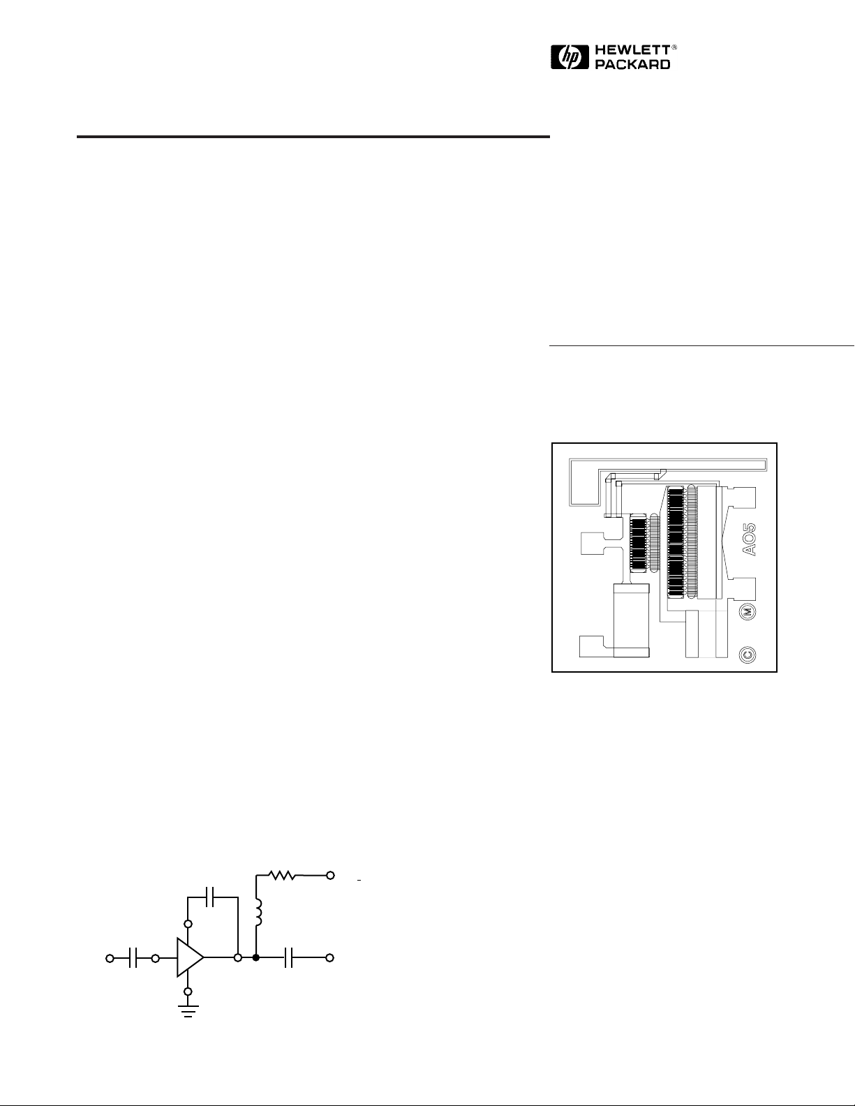
Chip Outline
[1]
flexibility.
Description
The MSA-0500 is a high performance, medium power silicon
bipolar Monolithic Microwave
Integrated Circuit (MMIC) chip.
The recommended assembly
procedure is gold-eutectic die
attach at 400°C and either wedge
or ball bonding using 0.7 mil gold
wire.
This MMIC is designed for use as a
general purpose 50 Ω gain block.
Typical applications include
narrow and broad band IF and RF
amplifiers in industrial and
military systems.
Typical Biasing Configuration
R
RFC (Optional)
= 12 V
d
bias
C
C
Fbl
C
block
IN OUT
4
3
MSA
1
2
V
This chip is intended to be used
with an external blocking capacitor completing the shunt feedback
path (closed loop). Data sheet
characterization is given for a
(Required)
> 15 V
V
CC
block
45␣ pF capacitor. Low frequency
performance can be extended by
using a larger valued capacitor.
Note:
1. See Application Note, AN-S009:
“Silicon MMIC Chip Use” for
additional information.
[1]
5965-9579E
6-346
Page 2
MSA-0500 Absolute Maximum Ratings
Parameter Absolute Maximum
Device Current 225 mA
(TMS)
[2,3]
= 25°C.
␣>␣140 °C.
MS
than do alternate methods.
jc
3.0 W
Power Dissipation
RF Input Power +25 dBm
Junction Temperature 200°C
Storage Temperature –65 to 200° C
Notes:
1. Permanent damage may occur if any of these limits are exceeded.
2. T
Mounting Surface
3. Derate at 50 mW/° C for T
4. The small spot size of this technique results in a higher, though more
accurate determination of θ
[1]
Thermal Resistance
θjc = 20°C/W
[2,4]
:
Electrical Specifications
[1]
, T
A
= 25° C
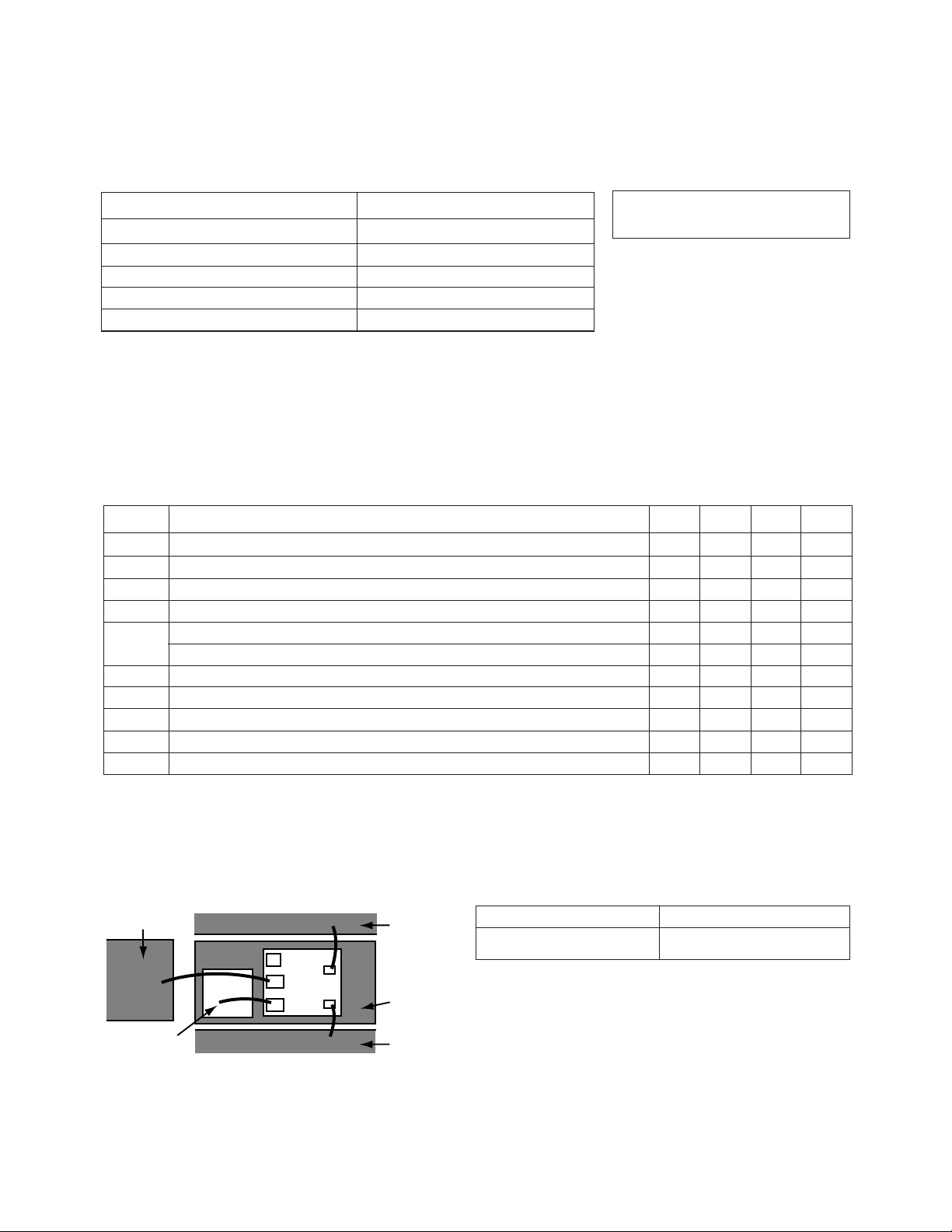
Unless otherwise noted, performance is for a MSA-0500 used with an external 45 pF capacitor. See bonding diagram.
Ground
Output
Trace
(backside
contact)
Ground
[2]
: Id = 165 mA, Z
= 50 Ω Units Min. Typ. Max.
O
GHz 2.8
Part Number Ordering Information
Part Number Devices Per Tray
MSA-0500-GP4 100
Symbol Parameters and Test Conditions
P
1 dB
G
P
∆G
f
3 dB
VSWR
IP
3
Output Power at 1 dB Gain Compression f = 1.0 GHz dBm 23.0
Power Gain (|S21|2) f = 0.1 GHz dB 9.0
Gain Flatness f = 0.1 to 2.0 GHz dB ±0.75
P
3 dB Bandwidth
3
Input VSWR f = 0.1 to 2.0 GHz 2.0:1
Output VSWR f = 0.1 to 2.0 GHz 2.5:1
Third Order Intercept Point f = 1.0 GHz dBm 33.0
NF 50 Ω Noise Figure f = 1.0 GHz dB 6.5
t
D
V
d
Group Delay f = 1.0 GHz psec 125
Device Voltage V 10.5 12.0 13.5
dV/dT Device Voltage Temperature Coefficient mV/°C –16.0
Notes:
1. The recommended operating current range for this device is 80 to 200 mA. Typical performance as a function of current
is on the following page.
RF performance of the chip is determined by packaging and testing 10 devices per wafer in a dual ground configuration.
2.
3. Referenced from 0.1 GHz gain (Gp).
Bonding Diagram
Input Trace
MSA
5
Die
2
1
A05
Capacitor
(45 pF typ)
4
3
Numbers refer to pin contacts listed on the Chip Outline.
6-347
Page 3

MSA-0500 Typical Scattering Parameters
0
2
4
6
8
10
14 16 18 20 22 24 26 28 30
POWER OUT (dBm)
Figure 1. Typical Gain vs. Power Out,
TA = 25°C, Id = 165 mA.
0.1 GHz
0.5 GHz
1.0 GHz
1.5 GHz
2.0 GHz
GAIN (dB)
Figure 2. Output Power @ 1 dB Gain
Compression, Third Order Intercept
Point, f = 1.0 GHz.
16
20
24
28
32
36
I
d
(mA)
80 120 160 200
IP
3
(dBm)
P
1dB
2.0 GHz
1.0 GHz
0.5 GHz
P
1dB
(dBm)
IP
3
+25–50 +100
16
18
20
22
24
26
28
G
p
(dB)
Figure 3. Output Power @ 1 dB Gain
Compression vs. Temperature,
Id = 165 mA.
CASE TEMPERATURE (°C)
FREQUENCY (GHz)
Figure 4. Gain vs. Frequency.
P
1 dB
(dBm)
0
4
8
12
16
20
4.0
0.1 0.2 0.3 0.5 2.01.0
Closed Loop
Open Loop
Freq.
S
11
S
21
[1,2]
(T
= 25° C, I
A
= 165 mA)
d
S
12
S
22
GHz Mag Ang dB Mag Ang dB Mag Ang Mag Ang k
0.001 .68 –8 15.6 6.05 176 –26.2 .149 25 .79 –7 0.92
0.005 .57 –38 14.6 5.37 186 –19.3 .108 38 .67 –35 0.56
0.010 .43 –65 12.8 4.38 158 –15.7 .165 30 .50 –61 0.64
0.050 .16 –111 9.8 3.08 164 –14.2 .194 10 .19 –101 1.06
0.100 .12 –134 9.3 2.90 169 –14.0 .200 4 .13 –117 1.11
0.200 .12 –141 9.1 2.86 168 –13.9 .202 4 .12 –125 1.13
0.400 .13 –133 9.1 2.84 162 –13.8 .204 4 .17 –116 1.10
0.600 .16 –124 9.1 2.84 155 –13.7 .207 4 .22 –109 1.05
0.800 .21 –118 9.0 2.83 148 –13.6 .210 5 .28 –108 0.99
1.00 .25 –115 9.0 2.83 139 –13.4 .213 6 .34 –106 0.91
1.50 .36 –113 8.8 2.75 118 –12.7 .232 9 .44 –107 0.72
2.00 .45 –120 8.2 2.58 96 –11.6 .262 12 .66 –111 0.39
2.50 .51 –125 7.3 2.32 83 –11.0 .281 17 .58 –109 0.43
3.00 .52 –134 6.0 2.00 66 –10.5 .297 18 .58 –109 .46
3.50 .51 –144 4.8 1.75 52 –9.6 .329 20 .58 –106 0.49
4.00 .46 –157 3.7 1.53 39 –9.2 .347 21 .54 –104 0.60
Notes:
1. S-parameters are de-embedded from 200 mil BeO package measured data using the package model found in the DEVICE MODELS
section.
2. S-parameter data assumes an external 45 pF capacitor. Low frequency performance can be extended using a larger valued capacitor.
Typical Performance, T
(unless otherwise noted)
= 25° C
A
6-348
Page 4

MSA-0500 Chip Dimensions
3
5
2
[1]
1
2
4
530 µm
20.8 mil
Unless otherwise specified, tolerances are
±13 µm/±0.5 mils. Chip thickness is 114 µm/4.5 mil.
Bond Pads are 41 µm/1.6 mil typical on each side.
Note 1: Output contact is made by die attaching the
backside of the die.
AK
570 µm
22.4 mil
6-349
 Loading...