

Page 1
Cascadable Silicon Bipolar
MMIC␣ Amplifier
Technical Data
MSA-0486
Features
• Cascadable 50 Ω Gain Block
• 3 dB Bandwidth:
DC to 3.2 GHz
• 8 dB Typical Gain at 1.0␣ GHz
• 12.5 dBm Typical P
1.0␣ GHz
• Unconditionally Stable
(k>1)
• Surface Mount Plastic
Package
• Tape-and-Reel Packaging
Option Available
Note:
1. Refer to PACKAGING section “Tapeand-Reel Packaging for Surface
Mount Semiconductors”.
[1]
1 dB
at
Description
The MSA-0486 is a high performance silicon bipolar Monolithic
Microwave Integrated Circuit
(MMIC) housed in a low cost,
surface mount plastic package.
This MMIC is designed for use as a
general purpose 50 Ω gain block.
Typical applications include
narrow and broad band IF and RF
amplifiers in commercial and
industrial applications.
The MSA-series is fabricated using
HP’s 10 GHz fT, 25␣ GHz f
silicon bipolar MMIC process
which uses nitride self-alignment,
ion implantation, and gold metallization to achieve excellent
performance, uniformity and
reliability. The use of an external
bias resistor for temperature and
current stability also allows bias
flexibility.
MAX
,
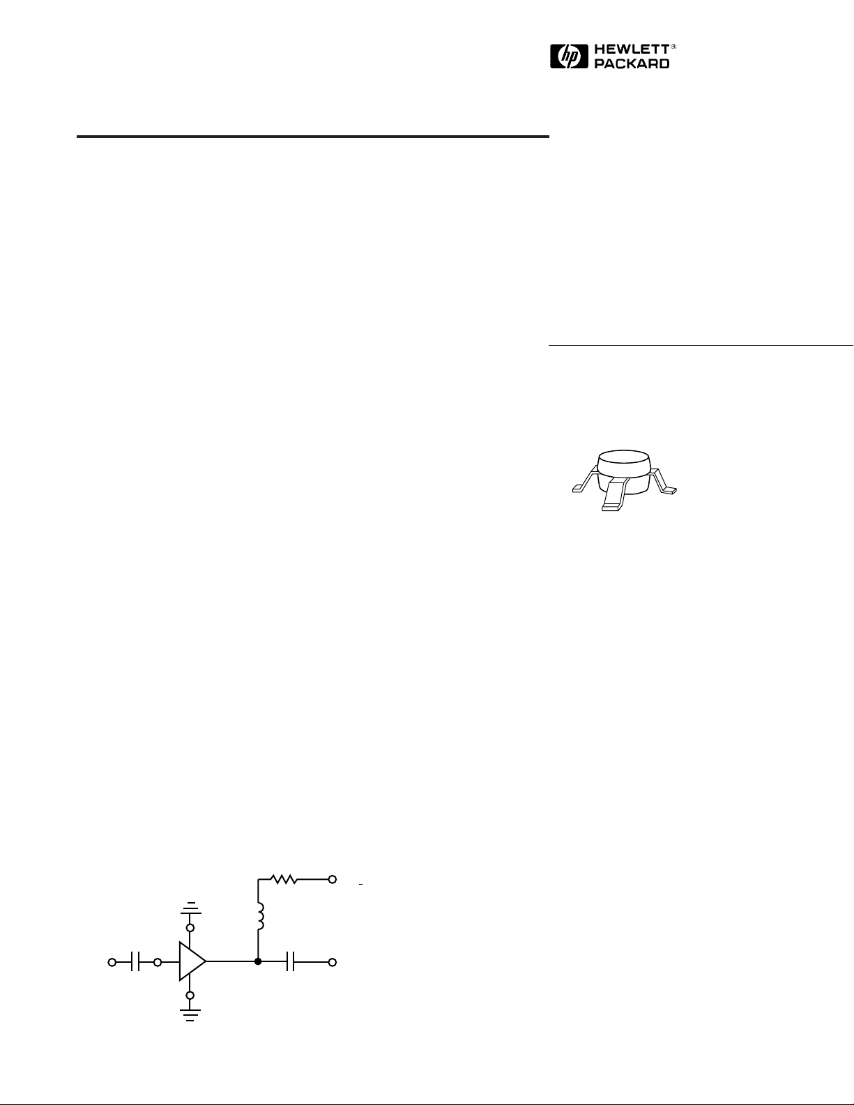
86 Plastic Package
Typical Biasing Configuration
R
bias
RFC (Optional)
C
block
IN OUT
4
3
MSA
1
2
V
d
= 5.25 V
C
block
5965-9578E
V
> 7 V
CC
6-342
Page 2
MSA-0486 Absolute Maximum Ratings
Parameter Absolute Maximum
Device Current 85 mA
Power Dissipation
[2,3]
500 mW
RF Input Power +13 dBm
Junction Temperature 150°C
Storage Temperature –65 to 150° C
[1]
Thermal Resistance
θjc = 100°C/W
Notes:
1. Permanent damage may occur if
any of these limits are exceeded.
CASE
= 25°C.
2. T
3. Derate at 10 mW/° C for T
4. See MEASUREMENTS section
“Thermal Resistance” for more
Electrical Specifications
[1]
, T
A
= 25° C
Symbol Parameters and Test Conditions: Id = 50 mA, Z
G
P
Power Gain (|S21|2) f = 0.1 GHz dB 8.3
= 50 Ω Units Min. Typ. Max.
O
information.
f = 1.0 GHz 7.0 8.0
∆G
f
3 dB
VSWR
Gain Flatness f = 0.1 to 2.0 GHz dB ±0.6
P
3 dB Bandwidth GHz 3.2
Input VSWR f = 0.1 to 3.0 GHz 1.5:1
Output VSWR f = 0.1 to 3.0 GHz 1.9:1
NF 50 Ω Noise Figure f = 1.0 GHz dB 7.0
P
IP
t
V
1 dB
3
D
d
Output Power at 1 dB Gain Compression f = 1.0 GHz dBm 12.5
Third Order Intercept Point f = 1.0 GHz dBm 25.5
Group Delay f = 1.0 GHz psec 140
Device Voltage V 4.2 5.25 6.3
dV/dT Device Voltage Temperature Coefficient mV/°C –8.0
Note:
1. The recommended operating current range for this device is 30 to 70 mA. Typical performance as a function of current
is on the following page.
[2,4]
:
> 100°C.
C
Part Number Ordering Information
Part Number No. of Devices Container
MSA-0486-TR1 1000 7" Reel
MSA-0486-BLK 100 Antistatic Bag
For more information, see “Tape and Reel Packaging for Semiconductor Devices”.
6-343
Page 3

MSA-0486 Typical Scattering Parameters (Z
6.5
6.0
7.0
7.5
8.0
FREQUENCY (GHz)
Figure 5. Noise Figure vs. Frequency.
0.1 0.2 0.3 0.5 2.01.0
NF (dB)
G
p
(dB)
0.1 0.3 0.5 1.0 3.0 6.0
FREQUENCY (GHz)
Figure 1. Typical Power Gain vs.
Frequency, TA = 25°C.
0
2
4
6
8
10
Gain Flat to DC
Id = 30 mA
Id = 50 mA
Id = 70 mA
V
d
(V)
Figure 2. Device Current vs. Voltage.
0
20
40
60
80
I
d
(mA)
2345671
TC = +85°C
TC = +25°C
TC = –25°C
6
7
8
11
12
13
–25 0 +25 +55 +85
7
8
9
P
1 dB
(dBm)
NF (dB)
NF
G
p
(dB)
TEMPERATURE (°C)
Figure 3. Output Power at 1 dB Gain
Compression, NF and Power Gain vs.
Case Temperature, f = 1.0 GHz,
Id=50mA.
P
1 dB
G
P
0.1 0.2 0.3 0.5 2.01.0 4.0
FREQUENCY (GHz)
Figure 4. Output Power at 1 dB Gain
Compression vs. Frequency.
3
6
9
12
15
18
21
P
1 dB
(dBm)
Id = 30 mA
Id = 50 mA
Id = 70 mA
Id = 30 mA
Id = 50 mA
Id = 70 mA
Freq.
S
11
S
21
= 50 Ω, TA = 25° C, I
O
S
12
= 50 mA)
d
S
GHz Mag Ang dB Mag Ang dB Mag Ang Mag Ang
0.1 .14 178 8.4 2.62 175 –16.2 .154 1 .16 –10
0.2 .14 175 8.3 2.61 170 –16.3 .153 2 .16 –20
0.4 .14 171 8.2 2.57 161 –16.3 .154 3 .17 –39
0.6 .13 168 8.1 2.54 151 –16.0 .158 4 .18 –57
0.8 .13 166 8.0 2.52 141 –15.9 .161 5 .20 –74
1.0 .13 165 7.9 2.48 131 –15.7 .165 6 .21 –88
1.5 .15 168 7.7 2.42 108 –14.8 .182 8 .27 –121
2.0 .21 168 7.3 2.32 84 –14.0 .199 7 .32 –149
2.5 .29 165 6.8 2.18 65 –13.1 .222 4 .38 –168
3.0 .37 153 5.9 1.97 43 –12.7 .231 –1 .40 173
3.5 .44 142 4.8 1.74 24 –12.5 .238 –5 .41 157
4.0 .50 130 3.6 1.52 7 –12.5 .238 –10 .41 145
5.0 .61 109 1.3 1.16 –21 –12.7 .231 –17 .43 132
A model for this device is available in the DEVICE MODELS section.
22
Typical Performance, T
(unless otherwise noted)
= 25° C
A
6-344
Page 4

86 Plastic Package Dimensions
0.51 ± 0.13
(0.020 ± 0.005)
RF INPUT
1.52 ± 0.25
(0.060 ± 0.010)
0.66 ± 0.013
(0.026 ± 0.005)
0.30 MIN
(0.012 MIN)
GROUND
45°
1
GROUND
2.67 ± 0.38
(0.105 ± 0.15)
(0.085 ± 0.005)
DIMENSIONS ARE IN MILLIMETERS (INCHES)
A04
5° TYP.
2.16 ± 0.13
4
RF OUTPUT
AND DC BIAS
3
2.34 ± 0.38
(0.092 ± 0.015)
2
(0.006 ± 0.002)
8° MAX
0° MIN
0.203 ± 0.051
C
L
6-345
 Loading...