

Page 1
MH89792
E1Transceiver
Preliminary Information
Features
• Complet e primary ra te 20 48kb /s CEPT line
driver and re ceiver
• Onboard pul se tran sform ers for transm it and
receive
• Meets lates t E TSI requirement s (ET S I ETS 30 0
011 (NET 5))
• Inductorless clock recovery
• Loss of signal indication/ polarity selection
• Programmab le pol arit y of extra cted c lock &
receive data
• Single +5 V ope ration
• Compatible with all E1 framers
2
• Small footprint area (<330mm
)
Applications
• Primary rate ISDN network Interface
• Multiplexe r equ ipm ent
• Private Network links
• Isochrono us LA NS/WANS
ISSUE 3 April 1995
Ordering Information
MH89792-1 20 Pin SIL Package
MH89792-2 20 Pin SIL Package
MH89792-3 20 Pin SIL Package
0°C to 70°C
Description
The Mitel MH89792 is a low cost E1 line driver/
receiver with clock extraction requiring no external
components. There are three versions available:
MH8979 2- 1 fo r 120
MH89792-2 for 75
MH8979 2- 3 fo r 100
Ω twisted pair cable;
Ω co-axial links;
Ω digital twisted pair.
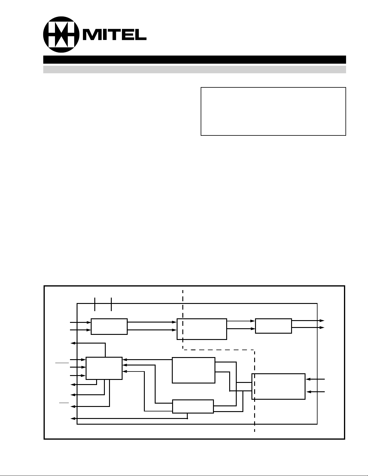
TxA
TxB
E2o
LOSP
CLKF/
CLKR
RxINV
RxA
RxB
LOS
RxD
VDD VSS
Line
Driver
Polarity
Selection
Clock/Data
Transmit
Isolation
Transform er
Clock
Recovery
Line
Receiver
EQUIPMENT SIDE
Figure 1 - Functional Blo ck Diag ram
6dB
Pad
Receive
Isolation
Transformer
LINE SIDE
TLA
TLB
RLA
RLB
4-223
Page 2
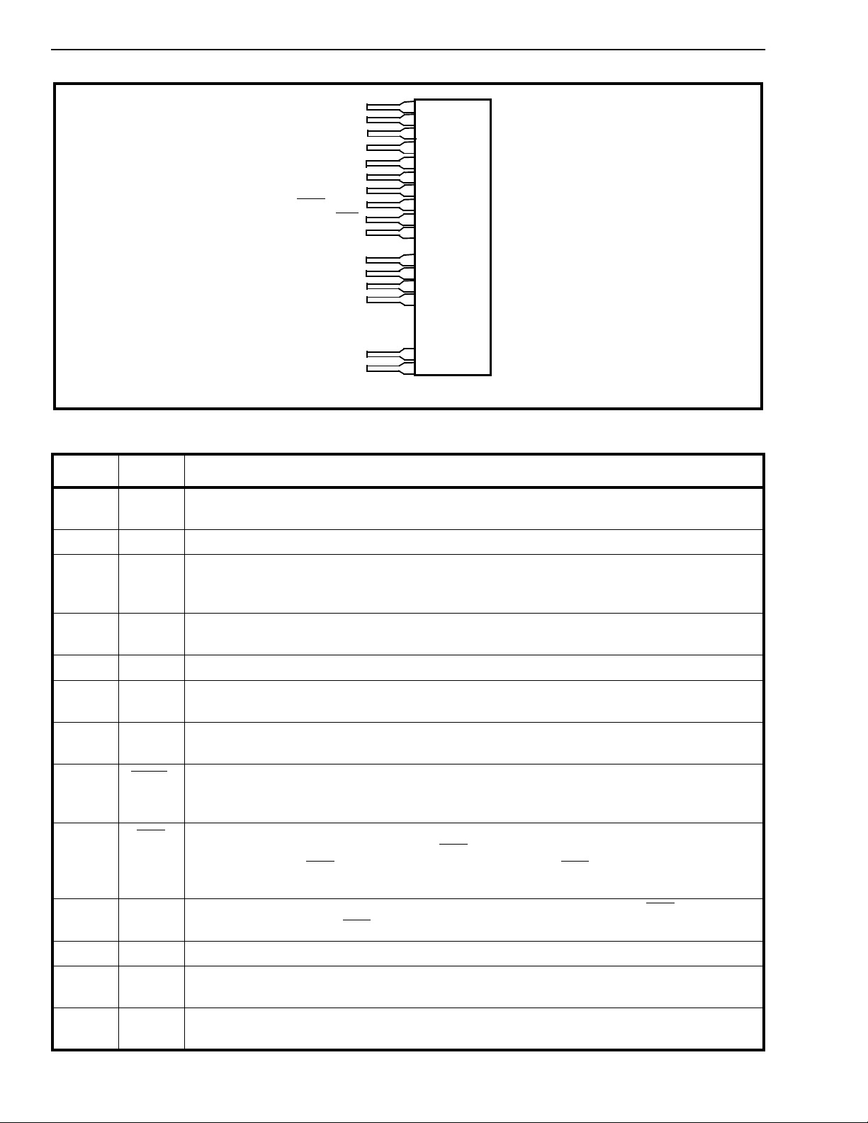
MH89792 Preliminary Information
1
2
3
4
5
6
7
8
9
10
11
12
13
14
15
16
17
18
19
20
CLKF
E2o
VDD
RxA
RxB
VSS
RxD
RxINV
/CLKR
LOS
LOSP
NC
RLA
RLB
TLA
TLB
NC
NC
NC
TxA
TxB
Figure 2 - Pin Connections
Pin Description
Pin # Name Description
1E2o2048kHz Extracted clock (Output). This clock is extracted by the device from the received
signal. It is used internally to clock in data received from RLA and RLB.
2V
D.C. Power (In pu t) +5V supply
DD
3RxAReceiver A (Output ). The bipolar CEPT signal received by the device at RLA and RLB
inputs is converted to a unipolar format and output at this pin. This pin should be connected
to the positive receive pin of the framer.
4RxBReceiver A (Output). This pin should be connect ed to the negati ve receive gain pin of the
framer and provides a signal of the same format as RxA.
5V
Ground (Input). D.C. power return path.
SS
6RxDReceiv ed Data (Outp ut) This unipolar return to zero format signal is the product of RxA
and RxB logically “OR” ed and is required by some framers.
7RxINVRxA/RxB inversion (Input). A logic low applied to this pin will invert the outputs RxA and
RxB. A logic high should be applied if no inversion is required.
8
CLKF/
CLKR
E2o phase selecti on is achieved by use of this pin. A logic low provides E2o with a
falling edge coinciding with the centre of the data bit. A logic high provides E2o with a rising
edge.
9
LOS
Loss of signal (Output). This pin goes low when 128 continuous zeros are received on the
RLA and RLB inputs. When RxINV and LOS
RxINV is high and LOS
is low RxA and RxB are forced low. LOS is reset when 64 ones are
are low RxA and RxB are forced high. When
received in two dual E1 framer periods.
10 LOSP Loss of signal Polarity (Input). A logic low applied to this pin will invert LOS. A logic high
should be applied when LOS
is required.
11 NC No connection. This pin is not fitted.
12 RLA Received Li ne A (In put). The A wire or Tip Connection of the E1 receive line should be
connected to this pin.
13 RLB Receive Line B (Input). The B wire or Ring connection of the E1 receive line should be
connected to this pin.
4-224
Page 3

Preliminary Information MH89792
Pin Description (Continued)
Pin # Name Des crip tio n
14 TLA Transmit Line B (Output). The B wire of Ring connecti on of the E1 receive line should be
connected to this pin.
15 TLB Transmit Line B (Output). The B wire or Tip connection of the E1 receive line should be
connected to this pin.
16 NC No Connection. This pin is not fitted.
17 NC No Connection. This pin is not fitted.
18 NC No Connection. This pin is not fitted.
19 TXA Transmit A (Input). A unipolar signal from the framer device used in conjunction with TxB
is used to generate the bipolar output signal.
20 TXB Transmit B (Input). A unipolar signal from the framer device used in conjunction with TxA
is used to generate the bipolar output signal.
Functional Description
The MH89792 is a E1 digital trunk interface which
when used with an approved framer will conform to
CCITT recommendation G.703 for PCM30 and I.431
for the ISDN. The functions provided include line
driver and receive circuitry, inductorless clock
recovery, data and clock polarity selection and loss
of signal indication.
Bipolar Line Receiver
The MH89792 receiver inter faces to the trans miss ion
line through an internal pulse transformer which
splits the received AMI lines signal into RxA and
RxB. These two signals are combined by internal
logic to form a new signal which represents the
received data, RxD. The signals RxA and RxB may
be inverted where required by applying a logic low
signal permanently to pin 7, (RxINV). RxD will not be
affected by use of this pin.
The input impedance seen by the transmission line is
about 120 oh ms when using the -1 var ian t fo r tw iste d
pair applications, about 75 ohms when using the -2
variant for coaxial cable applications, and is about
100 ohms when using the -3 variant for digital
twisted pair applications.
Attenuation of the transmission line shall not exceed
6dB (at 1024kHz) and attenuation characteristics
shall be close to the “square root of f”
Af (dB) = AF
Where:
AF - attenuation at frequency f in dB
- attenuation at frequency f
AF
ref
f
- reference frequency (in this case 1024) kHz
ref
f - frequenc y i n k H z
(dB)* √ f
ref
in dB (in kHz)
ref
f
ref
Bipolar Line Transmitter
The MH89792 transmitter interfaces to the
transmission line through an internal pulse
transformer which combines the TxA and TxB data
into an AMI line coded signal. This is then passed
through the 6dB pad prior to being applied to the
line.
Clock Extractor
The MH89792 contains a clock extraction circuit
which generates the E2o clock from the received
data without the use of external crystals or a tunable
inductor.
The edge of the E2o extracted clock approximately
aligns with the centre of the received data pulse and
can be configured as either rising or falling edge by
the use of pin 8. (CLKF/CLKR).
Loss of Signal
The circuitry on the MH89792 is capable of detecting
128 continuous ZEROs received on RLA and RLB
and indicating this condition as a logic low on pin 9,
(LOS)
. When LOS and RxINV are low RxA and RxB
are forced high, when LOS
RxA and RxB are forced low LOS
64 ONEs are received in a two E1 frame period. LOS
may be inverted by applying a logic low to pin 10,
(LOSP).
is low and RxINV is high
will not reset un til
4-225
Page 4

MH89792 Preliminary Information
INT
MH89792-1
DSTi
DSTo
CSTio
CSTo
CSTi1
MT8979
C2i
MT9042
MT8941
F0i
XSt
TxA
TxB
RxD
RxA
RxB
E2i
9
LOS
19
TxA
20
TxB
6
RxD
3
RxA
4
RxB
1
E2o
RxINV
7
V
V
SS
DD
5
+5V
Figure 3a - Application Ci rcuit
2
TLA
TLB
RLA
RLB
CLKF/
CLKR
LOSP
10
14
15
12
Twisted Pair
13
8
Twisted Pair
Coax Connection
-2 Version only
Coax Connection
-2 Version only
0.1µ
10K
8-15
18-22
VDD
33
2
32
23
24
25
7
1
RESET
DSTi
DSTo
E8Ko
MT9079
D0-7
AC0-4
R/W
CS
DS
IRQ
S/P V
36
TAIS
+5
3
4
1
MH89792-1
TxA
TxB
RxA
RxB
E2o
VDD
RLA
TLA
TLB
RLB
LOS
CLKF/CLKP
RXINV
LOSP
1641
43
42
35
19
20
30
29
27
31
26
MT9042
V
DD
TxMF
TxA
TxB
RxA
RxB
E2i
F0i
C4i
SS
37
12
14
15
13
9
10
+5
2
NETWORK
CONNECTOR
8
7
4-226
Figure 3b - Application Circuit
Page 5

Preliminary Information MH89792
ISOLATION BARRIER
MH89792
LINE
CONNECTORS
NETWORK
SIDE
NOTES: X = Pin not fitted
Separation across barrier > 2mm recommended.
20
1
SYSTEM
SIDE
PLL
FRAMER
Side View
Notes
1)Not to scale
2)Dimensions in inches
3)(Dimensions in millimeters)
* Dimensions to pin center &
tolerance non accumulative.
(2.5 Max)
0.27 Max
(6.9 Max)
Figure 3c - Application Ci rcuit
0.1 Max
0.56 Max
(14.2 Ma x )
0.010 +
(0.25 +
0.05 +
(1.3 +
0.5)
0.00 2
0.05)
*
0.01
1
0.05 +
(1.225 +
*
0.02
0.05)
0.020 +
(0.51 +
2.0 + 0.040
1.0)
(50.8 +
0.005
0.13)
*
0.100 +
(2.54 +
*
0.01 0
0.26)
0.18 +
(4.6 +
0.02
0.5)
Figure 4 - Mechanic al Data
4-227
Page 6

MH89792 Preliminary Information
Notes:
4-228
 Loading...