

Page 1
MH88620BR
C.O. SLIC
Preliminary Info rm atio n
Features
• 900 ohm inp ut imp eda nce
• Externally s electa ble net work ba lanc es
• Transformerless 2-4 wire conversion
• Programmab le c onsta nt resis tan ce feed
• Off-Hook and Dial pulse detection
• High immunity to externally induced longitudinal
currents
• Auto ring trip
• On-hook tran smissi on (A NI) cap ability
• Minimum p rotecti on circ uitry requi red
• Compatible with require men ts of TEL EBR AS
DOC/FCC, CSA/UL, CCITT
• Excellent power dissipation (SIL vertical
mountin g)
Applications
• On/Off-Premise PBX Line Cards
• Central Offic e Line C ard s
ISSUE 3 April 1995
Ordering Information
MH88620BR 40 Pin SIL Package
0°C to 70°C
Descript io n
The Mitel MH88620BR SLIC provides all of the
functions required to interface 2-wire off premise
subscriber loops to a serial TDM, PCM, switching
network of a modern PBX. The MH88620BR is
manufactured using thick film hybrid technology
which offers high voltage capability, reliability and
high density resulting in significant printed circuit
board area savings. A complete line card can be
implemented with very few external components.
V
AGND
EE
2W/4W
conversion
GTX0GTX1RX
Ring
Filter
TX
SHK
N1
N2
RING
RF1
RF2
TIP
TF1
TF2
TRD
V
Bat
Matched
Resistors
Test Relay
Driver
TRC
LGND
Feed
Auto Ring
Trip
RGND
VRLY
Driver
Circuitry
and
Speech
Circuit
Ring Relay
Driver
RNGC
RRD
LCA
Loop
Current
Set
Impe dance
Network
Z2Z1
Switch-Hook
Detect
GRX1
GRX0
V
DD
Switch-Hook
Thre sh ol d Set
Gain Adjust
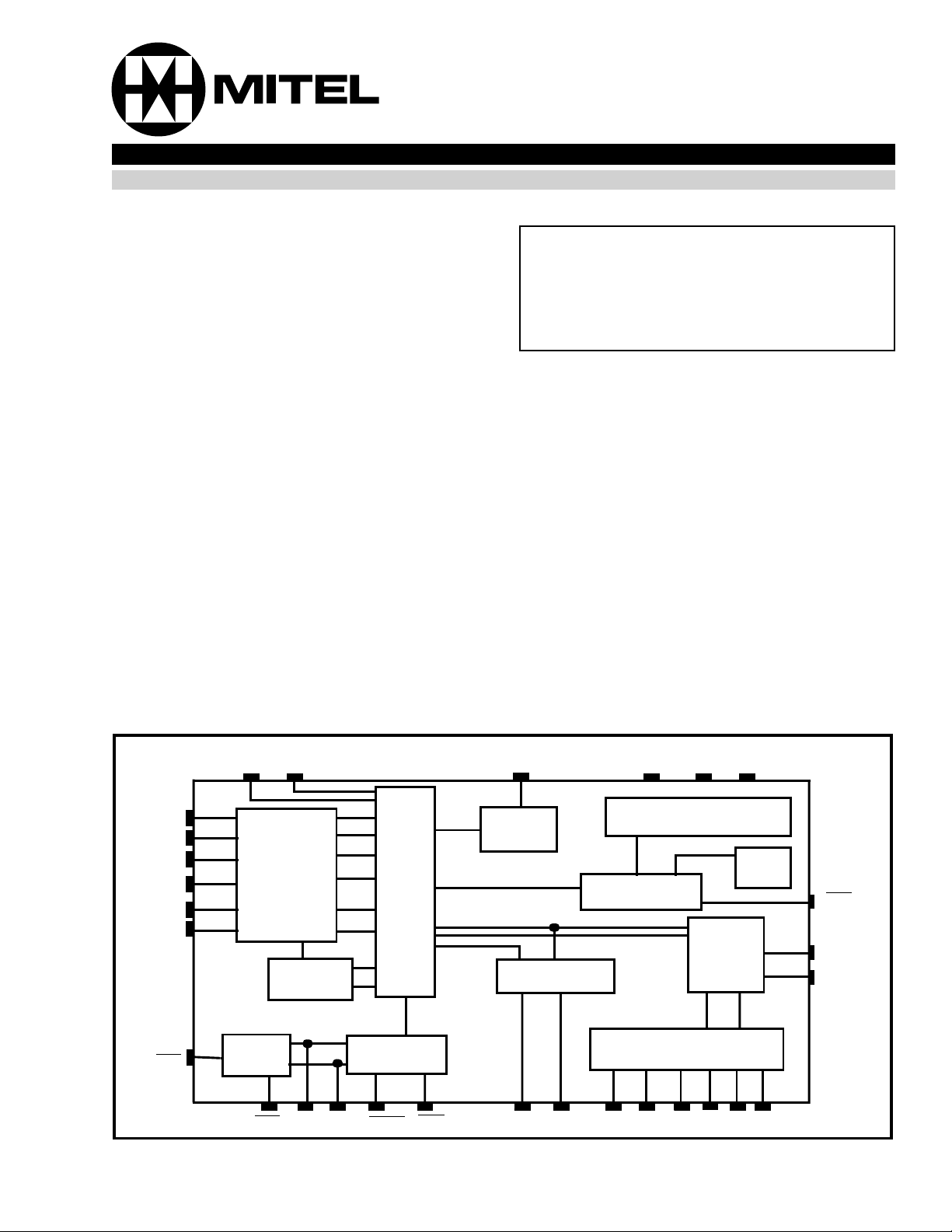
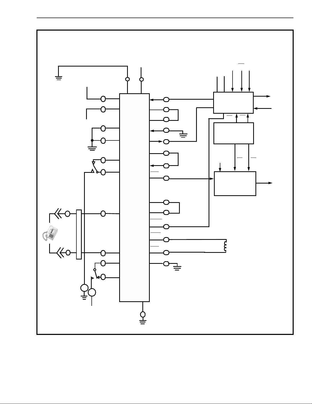
Figure 1 - Functional Block Diagram
2-145
Page 2
MH88620BR Preliminary Information
TIP
RING
TF1
TF2
RF1
RF2
LGND
LCA
VBA T
IC
RGND
VRLY
RRD
RNGC
REVC
ESI
ESE
AGND
NATT
N1
1
2
3
4
5
6
7
8
9
10
11
12
13
14
15
16
17
18
19
20
N2
NC
Z1
Z2
TX
RX
GTX0
GTX1
GRX0
GRX1
NC
NC
NC
SHK
IC
IC
IC
IC
VEE
VDD
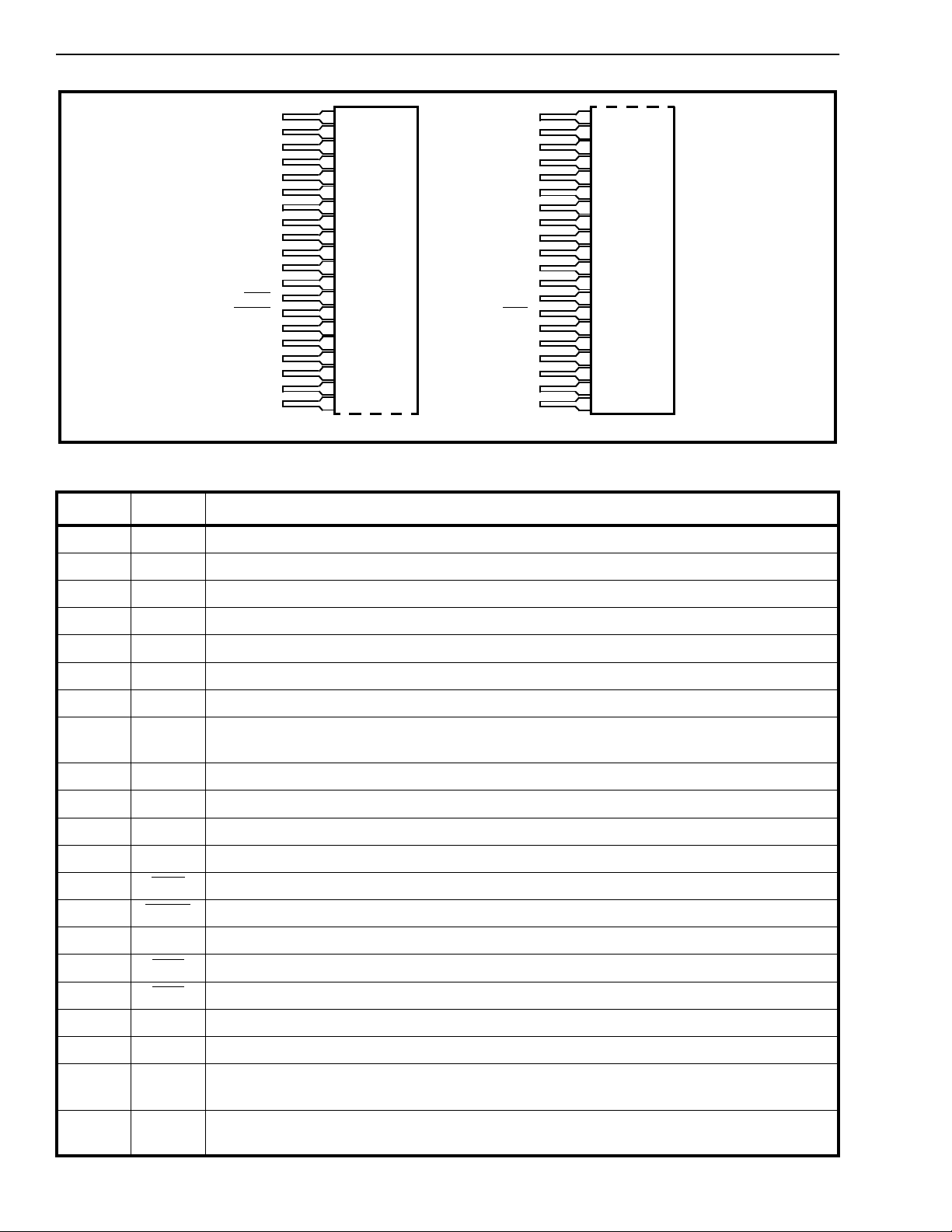
Figure 2 - Pin Connections
Pin Description
Pin # Name Description
1TIPTip Lead. Connect s to the TIP lead of the subscriber line.
21
22
23
24
25
26
27
28
29
30
31
32
33
34
35
36
37
38
39
40
2 RING Ring Lead: Connects to the Ring lead of the subscriber line.
3TF1Tip Feed 1: Access point for balanced ringing. Normally conne cts to TF2.
4TF2Tip Feed 2: Access point for balan ced ringing. Normally connects to TF 1.
5RF1Ring Feed 1: Access point for balanced ringing. Normally connects to RF2 .
6RF2Ring Feed 2: Access point for balanced ringing. Normally connects to RF1 .
7LGNDBattery Ground. V
return path. Connected to system’s energy dumping ground.
Bat
8LCACurren t Limit Set (In put): The current limit is set by connecting an external resistor as
shown in Table 5. For 70mA default current, this pin is tied to -5V.
9V
Bat
Battery Vo ltage: Ty pi cally -48V dc is applied to this pin.
10 NC No Connection: Reserved.
11 RGND Ring Driver Ground Connection.
12 VRLY Relay Supply Voltage Connection.
13 RRD
14 RNGC
Ring Relay Dri ve (Ou tp ut). Connects to ring relay coil.
Ring Relay Co ntro l (Input) .
15 NC Reserved. No Connection.
16 TR D
17 TR C
Test Relay Drive (Output ): Connects to test relay coi l.
Test Relay Control (Inp ut).
18 AGND Analog G r oun d: V
and V
DD
return path.
EE
.
19 NC No Connection: Reserved.
20 N1 Network Balance Node 1. An external network balance impedance can be connected
between N1 and AGND. See Fig 4. For complex impedances N2 no connection.
21 N2 Network Balance Node 2. An external network balance impedance can be connected
between N2 and AGND. See Fig 4 N2 connects to GND for 900Ω balance.
2-146
Page 3

Preliminary Information MH88620BR
Pin Description (Continued)
Pin # Name Description
22 NC No Connection. Reserved.
23 Z1 Line impedance Node 1. Normally connects to Z2. See Fig. 3.
24 Z2 Line impedance Node 2. Normally connects to Z1. See Fig 3.
25 TX Transmit (Output)
26 RX Receive (Input). 4-wire (AGND) referenced audio input.
27 GTX0 Transmit Gain Node 0. Connects to GTX1 for 0dB transmit gain.
28 GTX1 Transmit Gain Node 1. Connects to a resistor to AGND for transmit gain adjustment .
29 GRX0 Receive Gain Node 0. Connects to GRX1 for 0dB gain.
30 GRX1 Receive Gain Node 1. Connect to a resistor to AGND for receive gain adjustme nt.
31 NC No Connection. Reserved.
32 NC No Connection. Reserved.
33 NC No Connection. Reserved.
34 SHK
35.38 IC Internal Connection.
39 VEE Negati ve Su pp ly Voltage. -5V dc.
40 VDD Positive Supply voltag e. +5V dc
Off-Hook Indicati on (Outpu t). A logic low output indicates when the subscriber
equipment has gone Off-Hook.
. 4-wire (AGND) referenced audio output.
2-147
Page 4
MH88620BR Preliminary Information
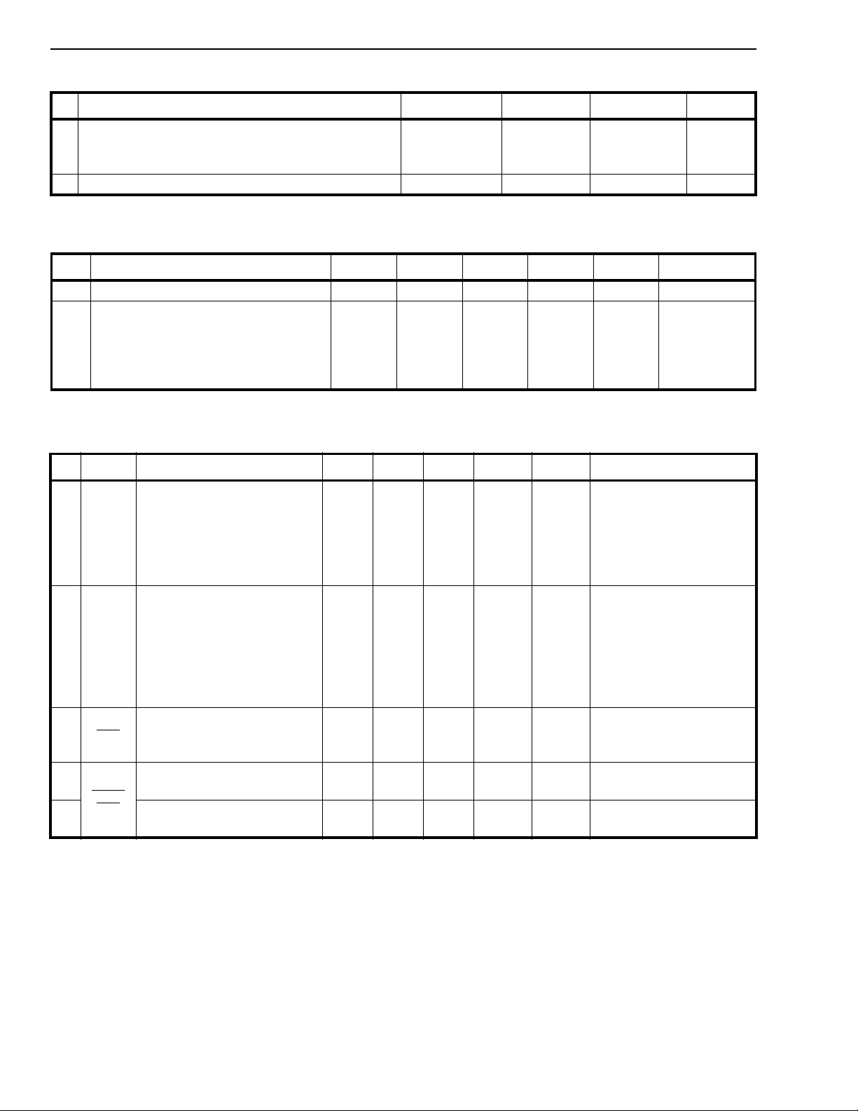
Absolute Maximum Ratings * All voltages are with respect to GNDA unless otherwise stated.
Parameter Symbol Min Max Units
1 Supply Voltages LGND -V
V
GND - V
2 Storage Temp eratu re T
* Exceeding these values ma y cause perm anen t dama ge. Functi onal operati on und er these cond ition s is not implied.
DD -
Bat
GND
EE
S
-40 +125 °C
65
6
6
Recommended Operating Conditions† - Voltages are with respect to GNDA unless otherwise stated.
Characteristics Sym Min Typ* Max Units Comments
1 Operating Temperature T
2 Supply Voltages V
* Typical figures are at 25°C and are for design aid only; not guaran teed an d not subject to producti on testing .
† Voltages specified are with respect to LGND.
OP
Bat
V
DD
V
EE
V
RLY
070°C
-44
4.75
-4.75
-48
+5.0
-5.0
5
70
-60
5.25
-5.25
V
V
V
V
DC Electrical Characteristics*
‡
Characteristics Sym Min Typ
1
Operating Loop Current
I
Loop
17
16
Max Units Test Comments
70 mA
mA
mA
= 0Ω, LCA = -5V
R
Loop
1500Ω
2000Ω V
Bat
V
V
V
= -48V
Variat ion in Loop Current
I
Loop
±2
from nominal
2
3
SHK
4
RNGC
TRC
5
* DC Electrical Characteristics are over recommended operating conditions unless otherwise stated.
‡ Typical figures are at 25°C with nom inal ±5 V supplie s and are for desig n aid only.
Operating Current
Power Dissipation
Low Level Input Voltage
High Level Input Voltage
Low Level Input Voltage
High Level Input Voltage
Low Level Input Current
High Level Input Current
I
Bat
I
DD
I
EE
PDo
PD1
V
OL
V
OH
V
IL
V
IH
I
IL
I
IH
2
15
15
2
250
0.5 V
3.7
0.8 V
2.4
20
20
mA
mA
mA
mA
W
mW
V
V
µA
µA
= Open (On-hook)
R
Loop
On-Hook or Off-Hook
On-Hook or Off-Hook
Active
Stand-by/I dle
= 400µ A
I
OL
I
= 40µA
OH
VIL = 0.0V
= 5.0V
V
IH
2-148
Page 5

Preliminary Information MH88620BR
AC Electrical Characteristics*
Characteristi cs Sym Min Typ
1
Analog Tx Gain (T-R to TX) 0 dB Externally adjusta ble
2
Analog Rx Gain (RX to T-R) 0 dB Ex ter nally a djust abl e
3
Ringing Capability 25 V
4
On-hook Transmission
Signal input level
Gain 4
5
SHK Rise Time
Fall time
6
2 Wire Termination Im peda nce 900 Ω A djust able
7
Off-Hook Detect Threshold 10 mA
8
2-Wire Return Loss
Ω at T-R
900
Zin = 900Ω
t
R
t
F
20
26
20
‡
Max Units Test Com m en ts
R
RMS
Loop
= 1400Ω
Term. 6.8µF +200Ω
V
2.0
8
1
1
V
RMS
dB
msec
msec
dB
dB
dB
= -48V
Bat
T-R load = 10Ωk min.
Dial Pulse Detection
300-500Hz
500-2500Hz
2500-3400Hz
900Ω + 2.16µF at T-R
Zin = 900Ω
14
18
14
9
Longitudinal Balance
Longitudinal to Metallic 58
55
53
10
Longitudinal Current Capabil ity 40 mA 20mA per lead
11
Idle Channel Noise
8
12
12
Transhybrid Loss
Tx gain 0dB
Rx gain 0dB
Rx to T-R
T-R to Tx
N
CR
N
CX
THL
16
20
16
13
14
Analog Signal Overload Level at
TIP and RING 4 dBm
15
Ringing Signal Voltage 70 80 90 V
16
Ringing Frequency 20 25 30 Hz
17
Ring Trip Delay 100 ms
18
Absolute Gain variation -25 0 +.25 dB 0dBm at T-R, 1kHz
19
Relative Gain, reference to 1kHz -2 0 +.2 dB 300-3400Hz
20
Power Supply Rejection Ratio
V
Bat
V
DD
V
EE
* AC Electrical Characteristics are over Recommended Operating Conditions unless otherwise stated.
‡ Typical figures are at 25°C with nomina l +
Note: Test Conditions use a transmit and receive gain set to 0dB default and a Z
“Ref” indicates reference impedance which is equivalent to the termination impedance.
“Net” indicates ne two rk bala nce impe dance.
5V supplies and are for design aid only.
PSRR
24
24
24
30
30
30
value of 900Ω unless otherwi se stated .
in
dB
dB
dB
dB
dB
dB
300Hz
600-2000Hz
3400Hz
2000Hz, 1000Hz
2000Hz, 3000Hz
3400Hz
dBrnc
dBrnc
dB
dB
dB
300-500Hz
500-2500Hz
2500-3400Hz
T-R = 900Ω
= -48V
V
Bat
RMS
dB 1kHz, 100mVpp
2-149
Page 6
MH88620BR Preliminary Information
Transmit Gain (dB)
2-Wire to Tx 20log
(Tx/2-Wire)
+6.0 No Resistor
+4.0 38.3k Re sult s in 0dB ov eral l gain when use d wit h
+3.7 32.4k
0.0 Connect GTX0 to GTX1
-3.0
-6.0 3.32k
-12.0 1.43k
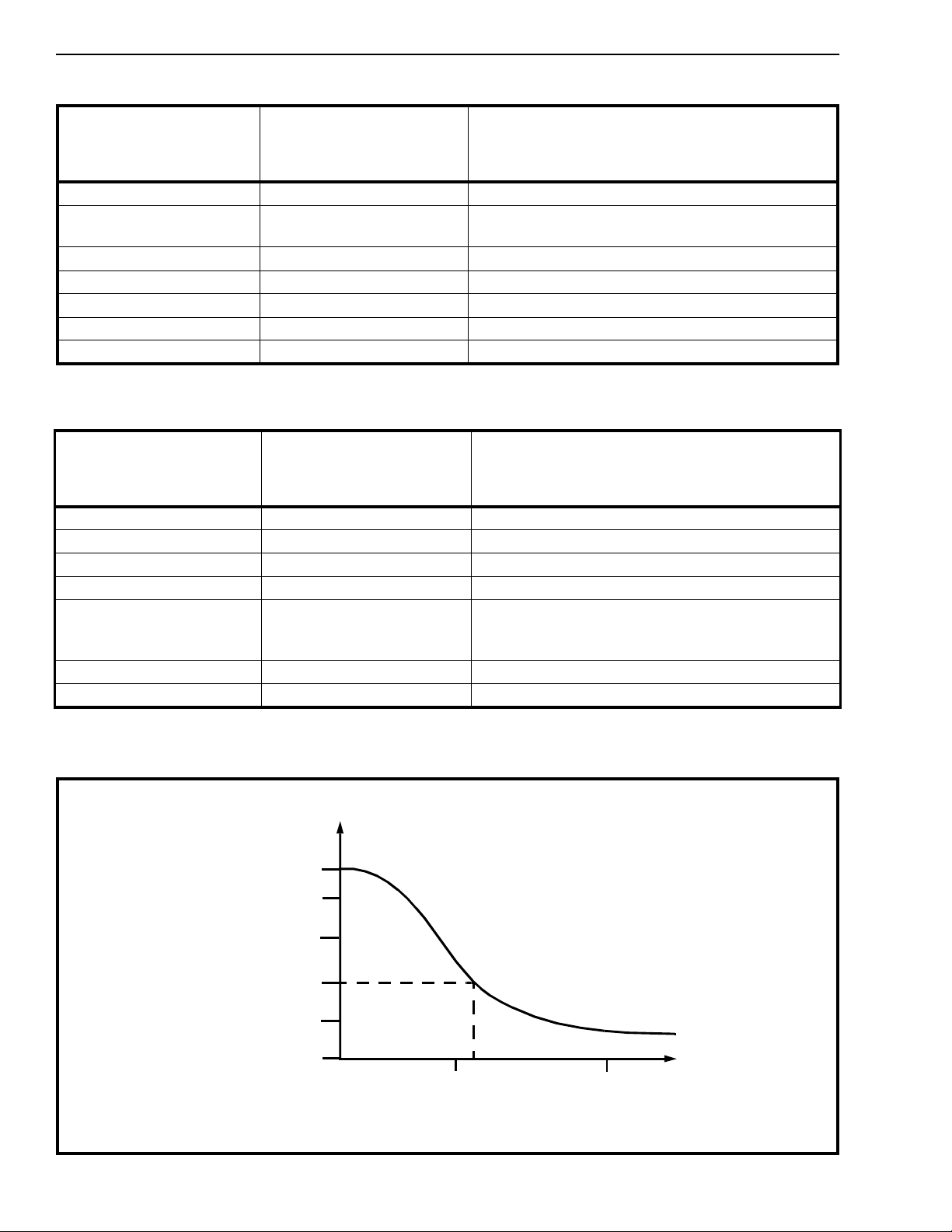
Note 1. Overall gain refers to the receive pat h of PCM to 2-Wire.
Note 2 See Figure 2 for Application Circuit.
Receive Gain (dB)
Rx to 2-Wire 20log
(2-Wire/ Rx)
RTX Resistor (1%)
Value ( Ω)
5.49k
RRX Resistor (1% )
Value (Ω)
Notes
Mitel A-law co dec (i.e. M T896 5)
Notes
+6.0 No Resistor
0.0 Con nect GRX 0 to GRX1
+3.0 5.49k
-3.7 4.87k
-4.0
4.64k Results in 0dB ov erall g ain wh en us ed with
-6.0 3.32k
-12.0 1.43k
Note 1. Ov erall gai n re fe rs to th e receive p ath o f PC M t o 2-W ir e .
Note 2. See Figur e 2 for Appli catio n Circ uit.
70
60
I
Loop
45
(mA)
30
15
Constant
Current
Region
0
Mitel A-law code c (i.e. M T89 65)
Constant
Voltage
Region
2-150
Graph 1 - I
1kΩ
Loop/RLoop
(ohms)
R
Loop
Characteristics
2kΩ
Page 7

Preliminary Information MH88620BR
Functional Description
The SLIC uses a transformerless electronic 2-4 wire
converter which can be connected to a Codec to
interface the 2 wire subscriber loops to a time
division multiplexed (TDM) pulse code modulated
(PCM) digital switching network. For analog
applications, the TXRX of the 2 wire converter can
be connected directly to an analog crosspoint switch,
such as the MT8816. Powering of the line is provided
through precision battery feed resistors. The
MH88620BR also contains control, signalling and
status circuitry solution which combines to provide
a complete functional solution, simplifying the
manufacture of line cards. This circuitry is illustrated
in the functional block diagram in Fig 1. The
MH88620BR is designed to be pin compatible with
Mitel’s MH88632, MH88625 and MH88628. This
allows a common PCB design with common gain,
input impedance and network balance.
Approvals
FCC part 68, CCITT, DOS CS-03, UL 1459, CAN/
CSA-22.2 N0. 225-M 9 0 and ANSI/EIA/T IA -4 6 4 -A ar e
system level safety standards and performance
requirements. As a component of a system, the
MH88620BR is designed to comply with the
applicable requirements of these specifications.
Battery Feed
The loop current for the subscriber equipment is
sourced through a pair of matched 200 ohm resistors
connected to the TIP and RING. The two wire loop is
biased such that the Ring lead is 2V above VBAT
(typically -46V) and the TIP lead is 2V below LGND
(typically -2V) during constant voltage mode.
bias voltage. The loop current is proportional to this
voltage. The loop c urrent can be set between 20 and
70 mA by various connections to the LCA pin as
illustrated in Table 5 and Figure 5. The loop current
during a fault condition will be limited to the constant
loop current programmed. Primary over current
protection is inherent in the current limiting feat ure of
the 200 ohm battery feed resistor. Refer to Graph 1.
Receive and Transmit Audio Path
The audio signal of the 2-wire is sensed diff erentially
across the 200 ohm feed resistor and is passed on to
a second differential amplifier stage in the 2W/4W
conversion block. This block sets the transmit gain
on the 4-wire side and cancels signals originating
from the rece ive in p ut .
Programmable Transmit and Receive Gain
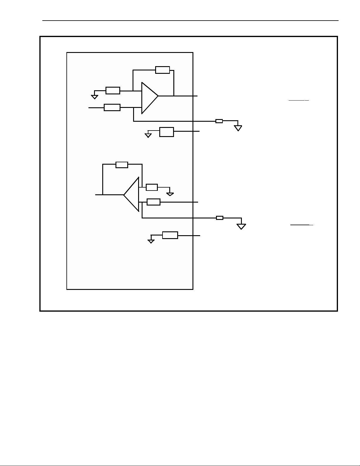
Transmit Gain (Tip-Ring t o Tx) and Receive Gain (Rx
to Tip-Ring) are programmed by connecting external
resistors (RRX and RTX) from GRX1 to AGND and
from GTX1 to AGND as indicated in Figure 2 and
Table 1 and 2. The programmable gain range is from
-12dB to +6dB; this wide range will accommodate
any loss plan. Alternatively, the default Receive Gain
of 0dB and Transmit Gain of 0dB can be obtained by
connecting GRX0 to GRX1 and GTX0 to GTX1. In
addition, a Receive Gain of +6dB and Transmit Gain
of +6dB can be obtained by not connecting resistors
RRX and RTX. For correct gain programming. the
MH88620BR’s Tip-Ring impedance (Zin) must match
the line termination impedance.
For optimum performance, resistors RRX should be
physically located as c lose as possible to the GRX 1
input pin, and resistor RTX should be physically
located as close as possible to the GTX1 input pin.
The SLIC is designed for a nominal battery voltage
of -48Vdc and can provide the maximum loop current
of 70mA under this condition.
The interface circuit is designed to be operated down
to a maximum of 16mA dc, with a battery volt age of
-44. The Tip and Ring output drivers can operate
within 2V of VBAT and LGND rails.
Loop Current Setting
The MH88620BR SLIC is a constant resistance with
constant voltage fallback design. This design feat ure
provides for long loop capability regardless of the
current setting. Refer t o graph 1.
The LCA (Loop Current Adjust) pin is an input to an
internal resistor driver network which generates a
Two Wire Port Termination Impedance
The AC termination of 900 ohms, of the 2W port is
set using active feedback paths to give the des ired
relationship between the line voltage and the line
current. The loop current is sensed differentially
across the two feed resistors and converted to a
single ended signal. This signal is fed back to the
Tip/Ring driver circuitry such that impedance in the
feedback p at h g e ts re fle cted to th e two w ire p o r t.
The MH88620BR’s Tip-ring impedance (Zin) is
designed to be 900Ω, when used w ith 2 5Ω PT C’s as
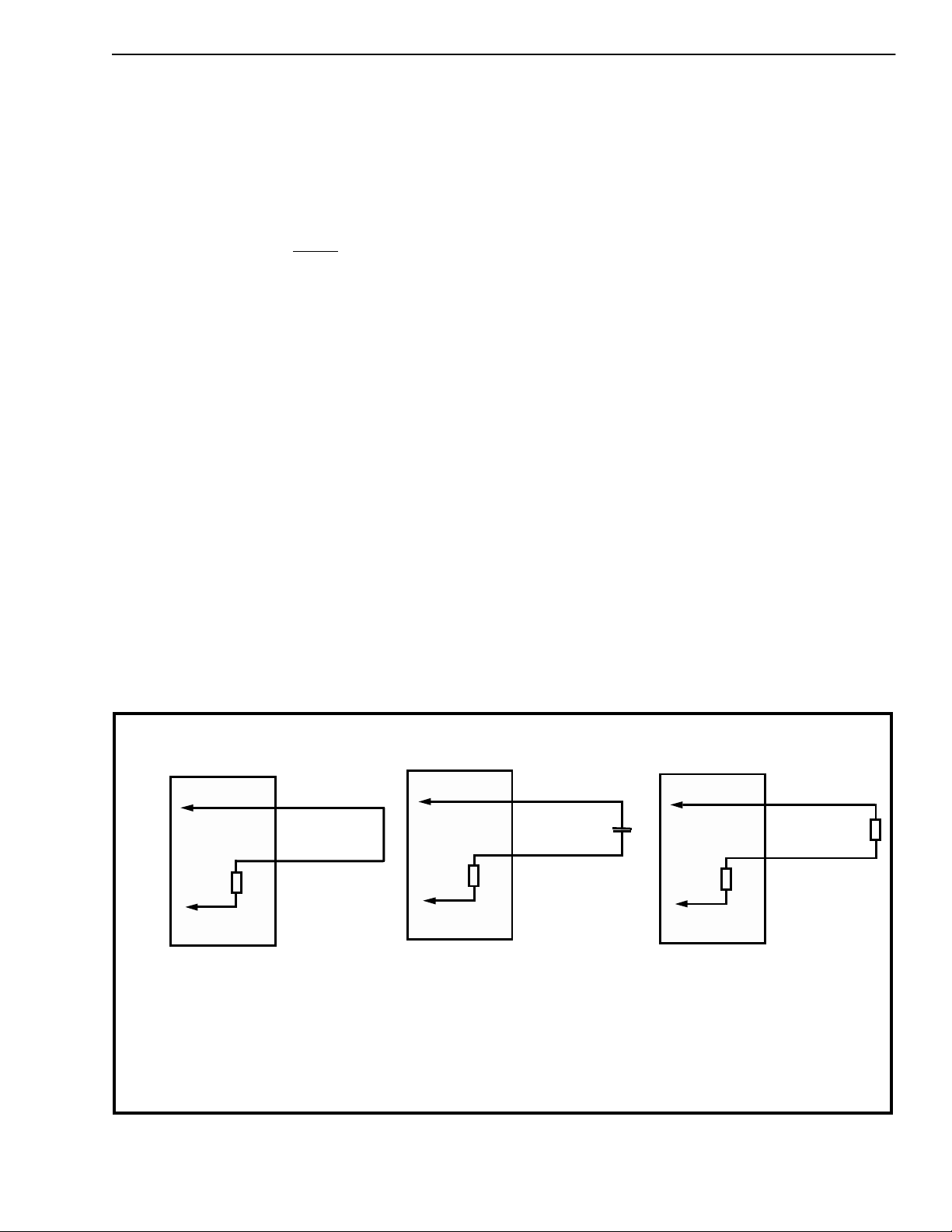
protection circuitry. For this requirement, Z1 and Z2
should be connected together on the PCB. To
accommodate the use of lower value PTC’s a series
resistance can be connected between Z1 and Z2.
For example, it two 8Ω PTCs are used, connect
2-151
Page 8

MH88620BR Preliminary Information
340Ω between Z1 and Z2. The design uses a 0.1
times impedance amplifier so the 340Ω actually adds
34Ω of additional impedance to the 850Ω (16 + 34 +
850 = 900). For complex impedance setting, a
capacitor and/ or resistor can be c onnected between
Z1 and Z2. For example, if Return Loss is to be
maximised for a Zin of 900 +2.2µF, a 0.22µF cap can
be connected between Z1 and Z2.
Networ k Balan ce
Transhybrid loss is maximised when the line
termination impedance and SLIC network balance
are matched. The MH88620BR’s network balance
impedance can be set to Zin, or to a user selectable
value. Thus, the network balance impedance can be
set to any Brazilian or other international
requirement. An external Network Balance
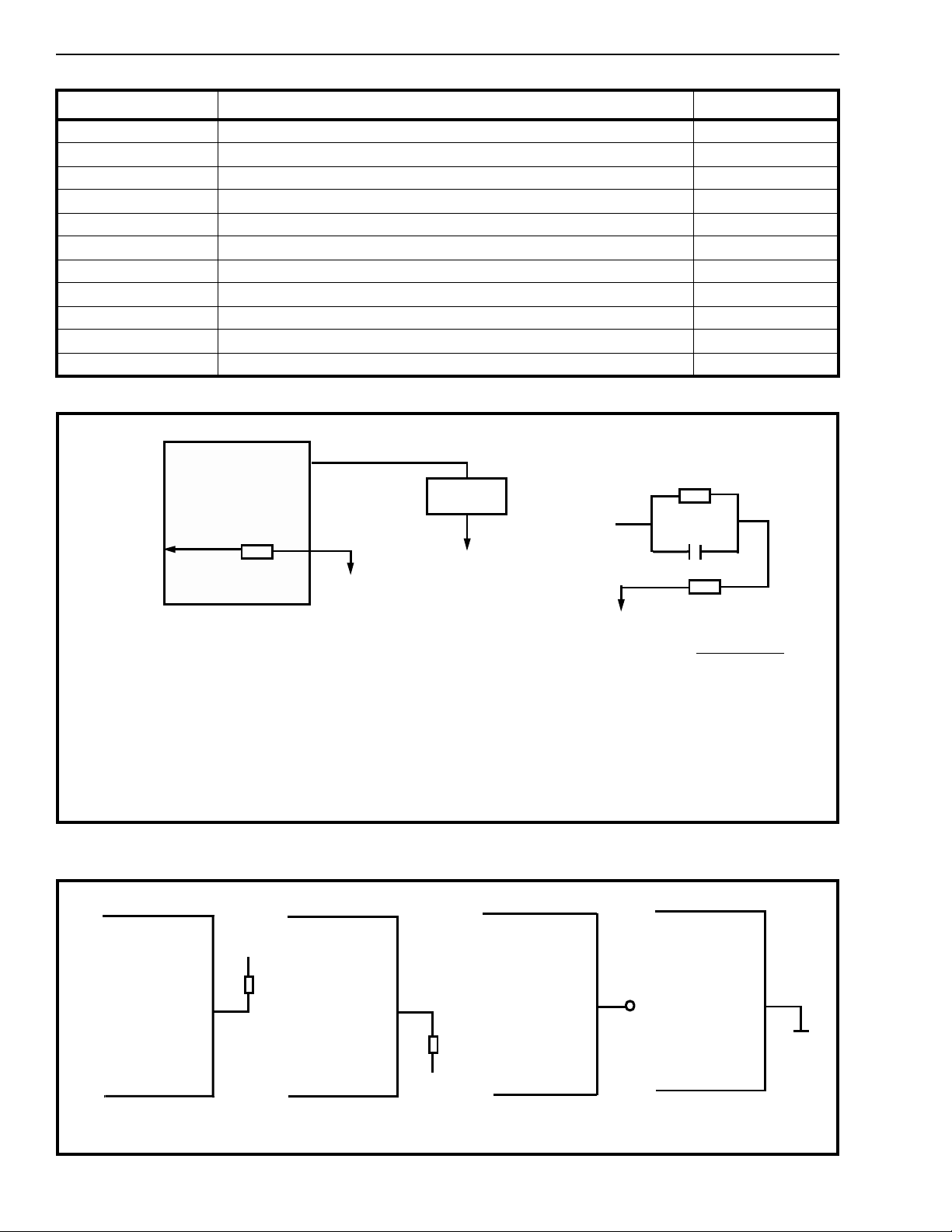
impedance is selected which 0.1 times the
impedance between N1 and AGND. N2 to GND
balances to 900Ω.
Off-Hook and Dial Pulse Detect ion
The SHK pin goes low when the DC-loop current
exceeds a specified level. The threshold level is
internally set by the bias voltage of the switch-hook
detect c ircu itry.
Dial pulses can be detected by monitoring the
interruption rate at the SHK
would be debounced by the system software.
pin. These dial pulses
DTMF
The DTMF tones are transmitted and received at the
4-wire port.
High voltage Capabili ty
Inherent in the thick-film process is the ability of the
substrate to handle high voltage. The standard Mitel
thick-film process provides dielectric strengths of
greater than 1000 VAC or 1500 VDC. The thick-film
process allows easy integration of surface mount
components such as the high voltage bipolar power
transistor line drivers. This allows for simpler, less
elaborate and less expensive protection circuitry
required to handle high voltage transcients and fault
conditions caused by lightning, induced voltages and
power line crossings.
On-Hook Transmission
The MH88620BR provides for on-hook transmission
which support s features such as Automatic number
identificat ion (ANI). The ANI info rmation is a FSK or
DTMF signal originating from and sent by the C.O.
during the off period of the ringing voltage being sent
to the subscriber’s set. The signal is present during
the off period between the first and second ring. The
subscriber’s set decodes the identification signal and
displays the calling party’s number.
Loop Length
Ring Trip Detecti on
The interface permits detection of an Off-Hook
condition during ringing. If the subscriber set goes
Off-Hook when the ringing signal has been applied,
the DC loop current flow will be detected within
approximately 100msecs and the SHK
low. The ring relay is automatically disabled by the
internal hardware.
output will go
Longitudinal Balance
The longitudinal balance specifies the degree of
common mode rejection in the 2 to 4 wire direction.
Precision laser trimming of internal resistors in the
hybrid ensures good overall longitudinal balance.
The interface circuitry can operate in the presence of
induced longitudinal currents of up to 40 mA RMS at
60 Hz.
The MH88620BR can accommodate loop lengths of
up to 2000 ohms minimum (including the subscriber
equipment). This corresponds to approximately
8kmusing #26 AWG twisted pair or 15km using #24
AWG twisted pair.
2-152
Page 9
Preliminary Information MH88620BR
Applications
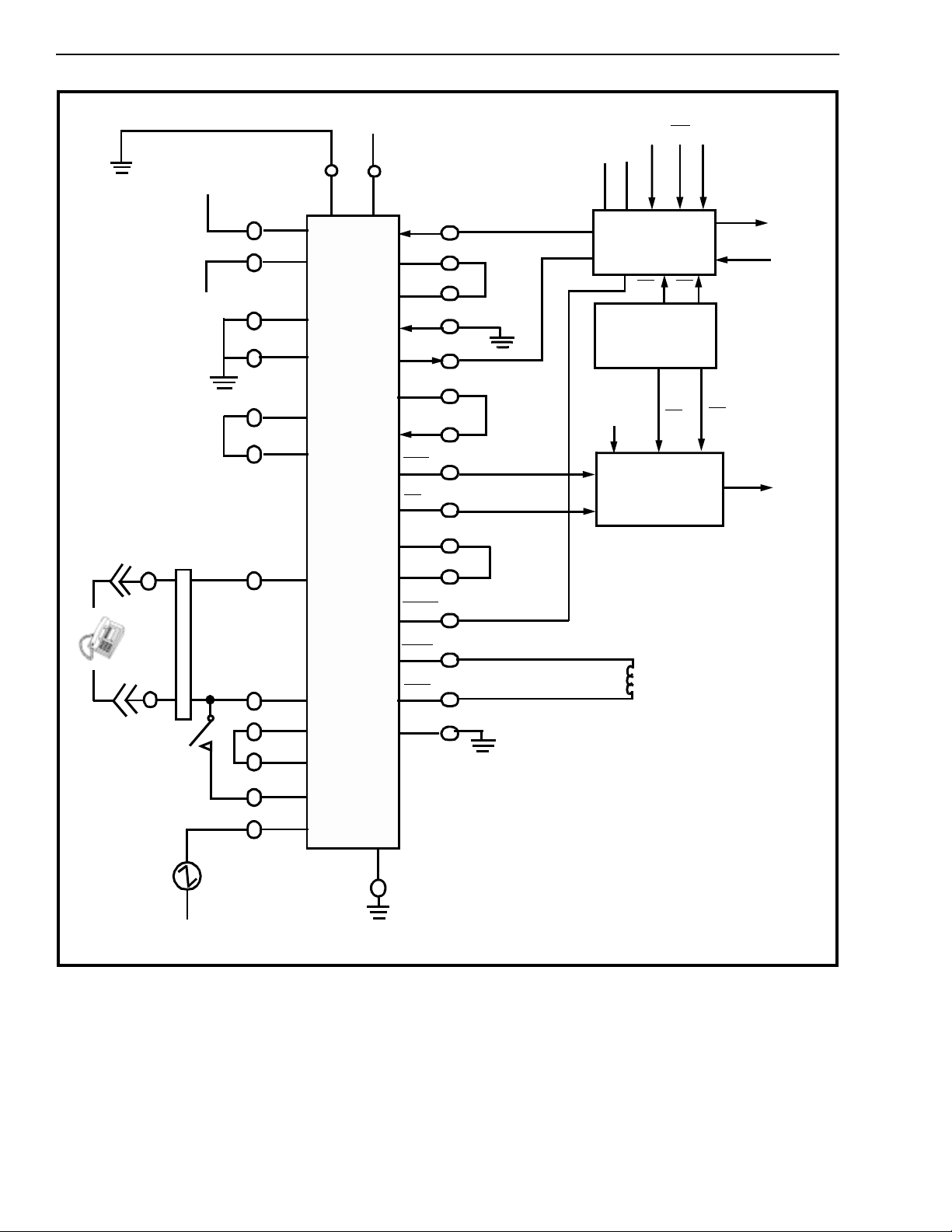
As shown in the application diagram, Figure 7, the
ringing voltage, typically 80 V
25Hz biased at
RMS
-VBAT, is applied to the subscriber line through an
external relay, K1, K1 is a DPST 2-form-C, EM
(electro-mechanical) relay which switches protection
diodes D3 and D4 out when Ringing is switched in,
K1 is enabled by applying a logic low level to the
relay driver control input, RNGC
.
An additional relay driver is provided to control an In/
Out Tes t Bus relay, K2. K2 is a DPST 2-fo rm-C, EM
relay which is enabled by applying a logic low level
to the relay driver control input.
Protection Circuitry
Primary protection, from lightning strikes and AC line
faults, is normally located in the MDF (main
distribution feeder) which is located external to the
PABX or CO switching system. The primary
protection circuitry is normally housed in a 5-pin
connector and consists of either carbon blocks, with
spark gaps (older technology), gas discharge limits
the high voltage to approximately 300 to 500 volts
before entering the switching system. Secondary
protection, in the switching system, is required to
further limit these high voltages/ currents. Secondary
protection is normally im plemented on each line card
and is designed to prot ect the SLICs from permanent
damage. The basic secondary high voltage
protection circuitry for the MH88620BR, as illustrated
in Figure 7, consists of PTC1, PTC2 and clamping
diodes D1 to D4. During a fault condition, the diodes
clamp the overvolt Ground and -VBAT. PTC1 and
PTC2 current limit as their resistance increases with
power dissipation caused by the over-voltage/
over-current condition. The ground that D1 and D3
are connected to, must be an EDG (energy dumping
ground) which is connected to the chassis or system
ground. This is a seperate conductor from LPGND or
AGND on the line card PCB. D2 and D4 conduct the
energy into a -VBAT supply which is a seperate
conductor from the -VBAT feed supply to the SLICs.
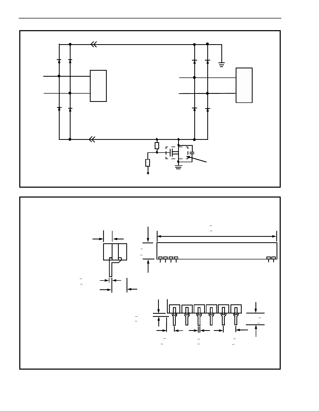
A power MOSFET circuit as shown in Figure 8, can
be used to divert the energy normally dumped into
-VBAT, the EDG conductor. Usually one MOSFET
circuit can be used for 16 SLICs or per line card.
Depending on the additional level of protection
required, PRO1 and/or PRO2 protectors may be
used. These are used to protect the SLICs Ring
sense resistor and/or Ring generator, from being
damaged if a fault condition occurs during the
application of Ringing to the line. PRO2 can be
implemented using two back to back zener diodes,
or an equivalent transcient suppressor.
The clamping voltage should be >16 Vdc and
<26Vdc. PRO2 may not be required depending on
the value and power dissipation of PRO1.
MH88620BR
24
Z2
R
Internal
8500 Ω
A.
Notes
a) to accommodate the use of 2 x 25Ω PTCs, connect Z1 and Z2 together, Z
b) to accommodate the use of 2 x 8Ω PTCs , c o nn ec t 3 40 Ω between Z1 and Z2 = 900Ω.
c) to accommodate the use of 2 x 25Ω PTCs, connect 0.22µF between Z1 and Z2 = 90 0Ω + 2. 2µ F.
23
Z1
Figur e 3 - Inp ut Im peda nc e (Z
MH88620BR
R
Internal
8500Ω
B.
Z2
Z1
24
23
External
0.22µF
= 900Ω.
in
) setting
in
MH88620BR
Internal
8500Ω
24
Z2
R
Z1
R
External
340Ω
C.
2-153
Page 10
MH88620BR Preliminary Information
Loop Current LCA Pin Connection Reference Fig #
20 Connect 10kΩ from LCA to +5V. 5a
25 Connect 16kΩ from LCA to +5V. 5a
30 Connect 36kΩ from LCA to +5V. 5a
35 Leave LCA open circuit 5c
40 Connect 24kΩ from LCA to -5V 5b
45 Connect 10kΩ from LCA to -5V 5b
50 Connect 5.6kΩ from LCA to -5V 5b
55 Connect 2.4kΩ from LCA to -5V 5b
60 Connect 1.3kΩ from LCA to -5V 5b
65 Connect 680kΩ fro m LCA to -5V 5b
70 Connect LCA to -5V 5d
Table 5 - Loop C urrent Se tting
MH88620BR
R Internal
9000 Ω
Notes:
1) The 10xZin network must be set to 10 x the desired input Zin (impedance).
2) The 10 x NETBAL network must be set to10x the desired network balance.
3) Make connection betwe en N1 and compone nt as short as possibl e.
N1
10 x
NETBAL
N2
Figure 4 - Ext ernal Netw ork Bal ance Se tting
RP
N1
Zin = 0.1 x RS+
where S = j x w
and w = 2 x JC x f
Example
If RS =0Ω, RP = 800Ω, CP=.5nf
Then the network balance is 800Ω in
parallel with 50nF.
CP
RS
[
:
1
1/RP + (S x CP)
]
2-154
5a
LCA
+5V
R
LCA
-5V
5b
Figure 5 - Loop Curren t Setting
5c
LCA
LCA
-5V
5d
Page 11
Preliminary Information MH88620BR
MH88620BR
Z
Transmit Gain:
(Tip-Ring to Tx)
AV= - 20log 0.5+3k
Example
RTX=38kΩ; AV= +4dBV
[
Ω
RTX
]
10kΩ
Z
GTX1
GTXO
10KΩ
Z
TX
25
28
27
RTX
Z
RX
30
29
26
RRX
Receive Gain:
(RX to Tip-Ring)
AV= -20log 0.5 + 5k
Example:
RRX=4.6kΩ; AV=-4dBV
10KΩ
GRX1
GRXO
10KΩ
Figure 6 - Gain Programmin g with Externa l Comp on ents
Ω
[
RRX
]
2-155
Page 12
MH88620BR Preliminary Information
-V
Bat
CSTi
+5
-5
FDi
C2i
SYSTEM
GROUND
+5V
-5V
V
DD
V
EE
TERM
BAT
RX
GRX0
GRX1
LCA
V
VR
VX
SDo
MT896X
CODEC
FLi
Ti meslot
DSTo
DSTi
CA
Assignment
AGND
TF1
TF2
P
R
O
T
E
C
T
I
O
N
TIP
RING
RF1
MH88620BR
TX
GTX0
GTX1
SHK
UD
Z1
Z600
RNGC
VRLY
RRD
REVC
C2i
Circuit
F1i
Status
Mux
Circuit
K1
CA
CSTo
2-156
RF2
RS1
RS2
NS
90V
-V
Bat
RMS
20Hz
Figure 7a - OPS SLIC Con fig urati on Appl ic atio ns Ci rcui t
Page 13
Preliminary Information MH88620BR
-V
Bat
CSTi
-5+5
FDi
C2i
SYSTEM
GROUND
+5V
-5V
V
DD
V
TERM
EE
V
RX
BAT
GRX0
GRX1
LCA
VR
VX
SDo
CODEC
SUBSCRIBER 1
CA
FLi
Timeslot
DSTo
DSTi
Assignment
AGND
TF1
TF2
MH88620BR
TX
GTX0
GTX1
SHK
Circuit
C2i
Stat us
Mux
F1i
CA
CSTo
Circuit
Z1
P
R
O
T
E
C
T
I
O
N
TIP
RING
RF1
Z2
RNGC
VRLY
RRD
REVC
K1
45V
RMS
20H z
RF2
45Vrms
20Hz
NS
~
+
~
+
-V
Bat
Figure 7b - OPS SLIC Configu rati on Appl ica tion s Circ ui t - Balanced Ringin g
2-157
Page 14
MH88620BR Preliminary Information
Energy Dump Ground (E.D.G)
Line 1
IN4004
IN4004
MH88620BR
TIP
Line 16
RING
10K
GD
1K
E.D.G
-48V
Figure 7c -16 Lines Ci rcui t Confi gu ratio n
S
10nF/100V
Heat Sink
9
IN4004
IN4004
o
C/w
MH88620BR
TIP
RING
Side View
0.010 +
(0.25 +
Notes:
1) Not to scale
2)Dimensions in inches).
3) (Dimensions in millimetres).
*Dimensio ns to centre of pin &
tolerance non ac cumulati ve.
0.002
0.05)
0.080 Max
(2.0 Max)
0.12 Max
(3.1 Max)
0.02
0.58+
(14.7+
0.05 +
(1.3 +
0.5)
0.01
0.5)
*
0.05 +
(1.3 +
2
3
1
43940
***
0.02
0.05)
Figure 8 - Mechanical Data
0.020 +
(0.51 +
4.20 + 0.020
0.5)
(50.8 +
0.05
0.13)
0.100 +
(2.54 +
0.10
0.13)
0.18 +
(4.6 +
0.02
0.5)
2-158
 Loading...