

Page 1
MH88600
Global SLIC
Preliminary Information
Features
• Programmable line impedance matching
• Internal complex i mp edance netw ork s
• Transformerless 2-4 wire conversion
• Programmable transmit/receive gain
• Accomm odat es worl dw ide trans miss ion
standards
• Opera tes with a wide range of ba tte ry volt ages
• Adjustab le c onsta nt curre nt ba ttery feed
• Overvol tag e and sho rt circu it pro tectio n
• Switch hoo k an d groun d bu tton de tectio n
• Ring tri p filte r and rel ay d river
• Low pow er co nsump tion
• High power dissipation capability during fault
conditions
Applications
Line interface for:
• PABXs
• Contr ol Sys tems
• Key Telephone Sy stems
• Central Office Equipment
ISSUE 7 April 1995
Ordering Information
MH88600 40 Pin DIL Hybrid
0°C to 70°C
Description
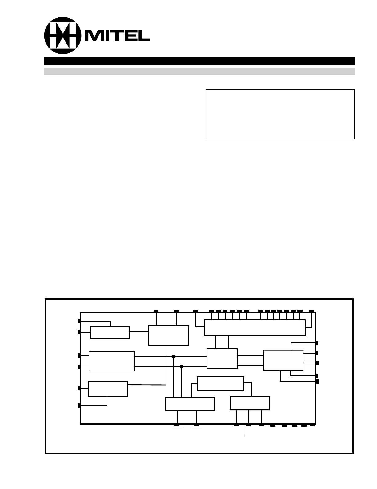
The MH88600 is a SLIC (Subscriber Line Interface
Circuit) which provides all of the BORSCH functions
of Battery Feed, Overvoltage Protection, Ringing
Feed, Line Supervision and 2-4 Wire Hybrid
conversion. In addition, the device matches the
many different line impedances specified by
regulatory authorities of around the world.
TF1
TF2
TIP
RING
RF1
RF2
Tip Drive
Over Voltage &
Short Circuit
Protection
Ring Drive
VREF
Constant
Current
Battery Feed
LCA
ZN14
Line Supervision
EGB
SHK
ZN13.................ZN8
Impedance Matchi ng Network
2-4 Wire
Hybrid
Circuit
Ring Trip Filter
Relay Driver
RC
ZN7.....................ZN1
RD
Figure 1 - Functional Block Diagram
Gain Adjust
VRR
GNDA
VDD
ZN0
PG2
PG4
TX
PG3
PG1
VEE
Vbat
GNDBat
2-83
Page 2
MH88600 Preliminary Information
40
ZN14
39
38
37
36
35
34
33
32
31
30
29
28
27
26
25
24
23
22
21
ZN13
ZN12
ZN11
ZN10
ZN9
ZN8
ZN7
ZN6
ZN5
ZN4
ZN3
ZN2
ZN1
TX
PG3
PG1
PG2
PG4
ZN0
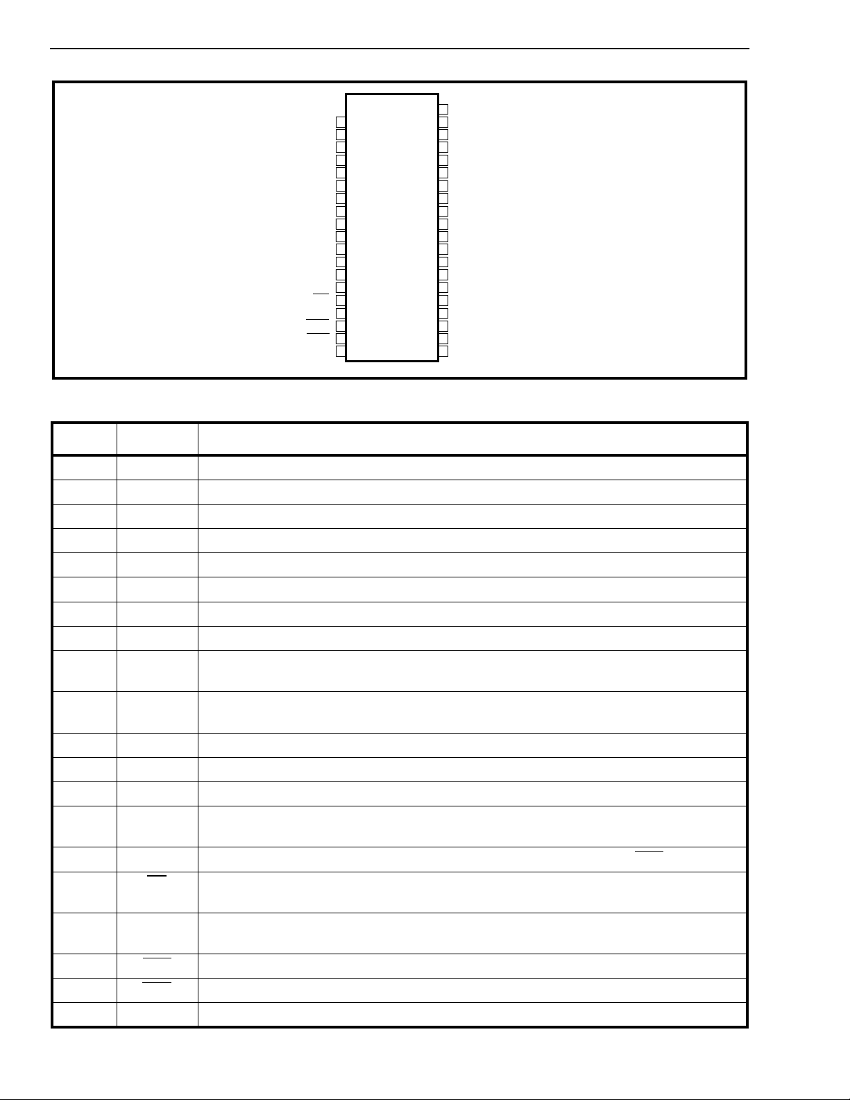
Pin Description
TIP
IC
RC
RD
2
3
4
5
6
7
8
9
10
11
12
13
14
15
16
17
18
19
20
VBat
RF1
RF2
RING
GNDBat
TF2
TF1
GNDA
VEE
VDD
VRR
LCA
SHK
EGB
VRef
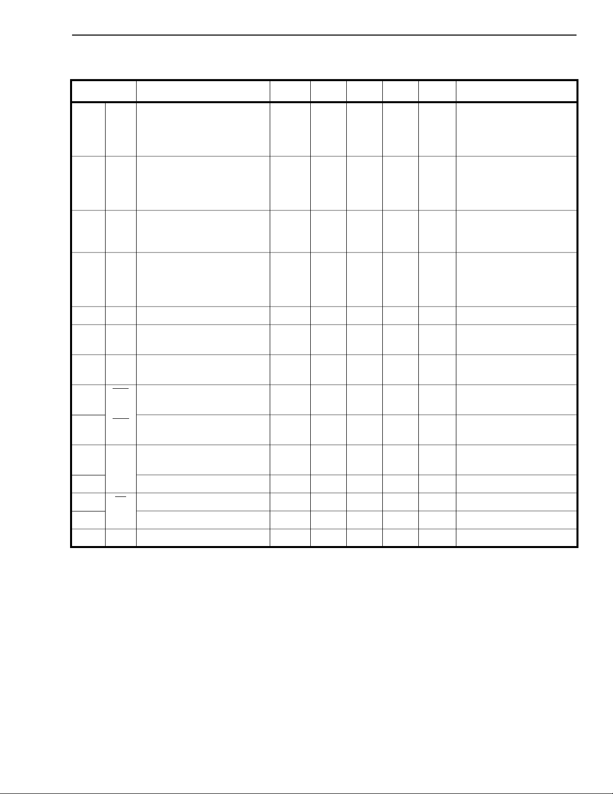
Figure 2 - Pin Connections
Pin # Name Description
1 No pin at this location.
2V
Bat
Battery Supply Voltage (Negati ve).
3RF1Ring Fe e d ( 1 ): Conne ct to relay contact. See Figures 6 & 7.
4
RF2
Ring Fe e d ( 2 ). Connect to relay contact. See Figu res 6 & 7.
5 RING Connects to the “Ring” or “B” lead of the telephone line.
6 TIP Connects to the “Tip” or “A” lead of the telephone line.
7I/CInternal Connection .
8GND
Battery Supply Ground (Positive ): Connect to System Ground
Bat
9TF2Tip Feed (2). Connect to TF1 for unbalanced ringing, see Figure 6. Connect to relay
contact for balanced ringing, see Figure 7.
10 TF1 Tip Feed (1). Connect to TF2 for unbalanced ringing, see Figure 6. Connect to relay
contact for balanced ringing, see Figure 7.
11 GNDA Analog Ground: Normally connected to System Ground.
12 V
13 V
14 V
EE
DD
RR
Negative Power Supp ly Voltage: Normally -5V.
Positive Pow er Su pp ly Voltage: Normally +5V.
Ringing Relay Cl am p Di ode : Connect to relay coil and to relay supply voltage
(Positive). For +5V relay, connect to VDD.
15 RC Ring Control (Input): A logi c hig h will activat e the Ri ng Relay D rive if SHK is high.
16 RD
Ring Relay Drive (Outpu t ). Connect to relay coil. A logic low will activate the relay by
sinking current from VRR through the relay coil.
17 LCA Loop Current Adjust (Input): Loop current is prop ortio nal to the vol tage at this input.
Normally connected to VRef
18 SHK Switch Hook Detect (Output): A logic low indicates an off-hook condition.
19 EGB
20 V
2-84
Ref
Earth Ground Button (Output ): A logic low indicates a grounded Ring lea d condition.
Voltage Reference (Output): Normally connected to LCA for default loop current.
Page 3

Preliminary Information MH88600
Pin Description (Contin ue d)
Pin # Name Description
21
ZN0
Impedance Node 0. Connect to external network for impedance (Zin) setting. See Table
2 and Figure 8.
22 PG4 Programming 4 (Input). Used for programmable gain and fo r default gain. Used as 4-
Wire Receive Input for default gain. See Table 3 and Figure 4 and 5.
23 PG2 Programming 2 (Input). U sed for programmab le gain. Used with resistor for 4-Wire
Receive Input. See Table 3 and Figure 4.
24 PG1 Programming 1 (Input). Used for programmable gain. See Table 3 and Figure 4.
25 PG3 Programming 3 (Input). Used for programmable gain and for default gain. See Table 3
and Figure 4 and 5.
26 TX 4-Wire Transmit Output:
27 ZN1 Impedance Node 1: Connect to other Impedance Nodes for impe dance (Z
see Table 1. Or , connect to external network for impedance (Z
) setting, see Table 2 and
in
) setting,
in
Figure 8.
28 ZN2 Impedance Node 2: Connect to other impedances Nodes for im pedance (Zin) setting.
See Table 1.
29 ZN3 Impedance Node 3: As per ZN2. S ee Table 1.
30 ZN4 Impedance Node 4: As per ZN2. S ee Table 1
31 ZN5 Impedance Node 5: As per ZN2. S ee Table 1
32 ZN6 Impedance Node 6: As per ZN2. S ee Table 1
33
ZN7
Impedance Nod e 7: As per ZN2. See Table 1
34 ZN8 Impedance Node 8: As per ZN2. S ee Table 1
35 ZN9 Impedance Node 9: As per ZN2. S ee Table 1
36 ZN10 Impedance Nod e 1 0: As per ZN2. See Table 1
37 ZN11 Impedance Nod e 11: As per ZN2. See Table 1
38 ZN12 Impedance Nod e 1 2: As per ZN2. See Table 1
39 ZN13 Impedance Nod e 1 3: As per ZN2. See Table 1
40 ZN14 Imp eda nce Nod e 14 : Connect to external net work for impedance (Z
Table 2 and Figure 8.
) setting. See
in
.
2-85
Page 4

MH88600 Preliminary Information
Functional Description
The BORSH Functions
The MH88600 performs all of the BORSH functions;
Battery Feed, Overvoltage Protection, Ringing,
Supervision and Hybrid.
Battery Feed
The MH88600 provides the loop with constant DC
current to power the telephone set. The voltage
(negative) applied at the LCA pin determines the
magnitude of the lop current.
I
= 3.731 x VLCA mA (±2mA)
Loop
Either the internal (V
voltage reference may be used to set the loop
current.
Overvol tage P rote ction
The MH88600 is protected from short term (20ms)
transients (+250V) between Tip and Ring, Tip and
ground, and Ring and Ground. However, additional
protection circuitry may be needed depending on the
regulatory requirements which must be met.
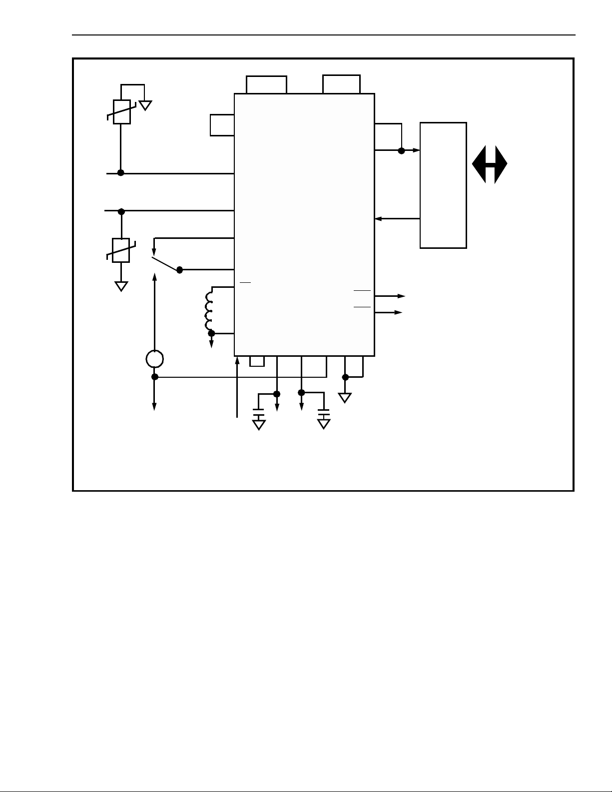
Normally, simple external shunt protection as shown
in Figures 6,7 and 8 is all that is required.
Ringing
The MH88600 has the capability to accommodate
both balanced and unbalanced ringing sources.
Refer to Figure 7 for the Balanced Ringing Circuit
and Figure 6 for the Unbalanced Ringing Circuit.
Supervision
The MH88600 is capable of detecting both Ground
Button and Switch Hook conditions. The Ground
Button detection (a logic low at the EGB
operates when an imbalance in Tip and Ring DC
current exceeds an internal threshold level caused
by a grounded Ring Lead. Use of the EGB
restricted to the off-hook condition of the telephone.
The Switch Hook detection operates (a logic low at
the SHK
an interna l th reshold level .
output) when the DC loop current exceeds
) or an external negative
Ref
output)
output is
Hybrid
The 2-4 Wire Hybrid circuit separates the balanced
full duplex signal at Tip and Ring of the telephone
line into receive and transmit ground referenced
signals at RX (receive) and TX (transmit) of the
SLIC. The Hybrid also prevents the input signal at
RX from appearing at TX. The degree to which the
Hybrid prevents the RX signal from appearing at TX
is specified at transhybrid loss.
Tip-Ring Drive Circuit
The audio input ground referenced signal at RX is
converted to a balanced output signal at Tip and
Ring. The output signal consists of the audio signal
superimposed on the DC Battery Feed Constant
Current. The Tip-Ring Drive Circuit is optimised for
good 2-Wire longitudinal balance.
Short Circuit Protection
The MH88600 is protected from long term (infinite)
short circuit conditions occurring between Tip and
Ring, Tip and Ground, Ring and Ground, and Ring
and Batte ry. The current is lim ited to the sam e v alue
as the Constant Current Battery Feed.
Programmable Line Impedanc e
The MH88600’s Tip-Ring (Zin) impedance can be
matched to the different impedances specified by
different telephone administrations worldwide. This
is accomplished by either linking specific pins as
specified in Table 1, or by adding external
components as shown in Figure 8 and Table 2.
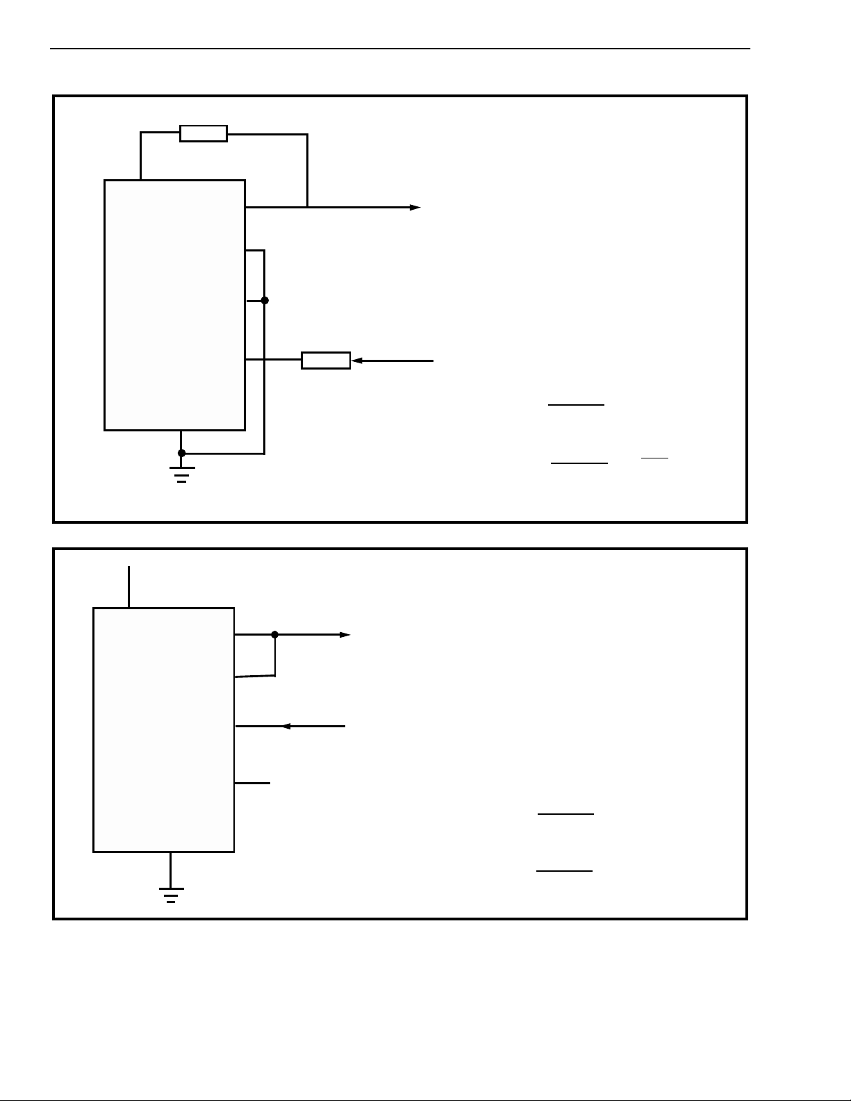
Programmable Transmit & Receive G ain
Transmit gain (TX to Tip-Ring) and Receive Gain
(Tip-Ri ng to RX) c an be prog ram med by conn ectin g
external resistors as indicated in Figure 4 and Table
3. Alternatively, the default Receive Gain of -4d Band
Transmit Gain of +4dB can be obtained by
connecting pins as shown in figure 5 and Table3.
Note that RX is not a pin on the SLIC. The RX
terminal will be either PG4 or the connection to the
receive gain programming resistor RRX shown in
Figure 4 and Figure 5.
The Ring Trip Detection Circuit prevents false offhook detection due to the current associated with the
AC ringing voltage and also due to the large current
transients when the ring voltage is switched in and
out. In addition , th e circu it pr ev e nt s con ne c ti on of the
ringing source during off-hook conditions.
2-86
Page 5
Preliminary Information MH88600
Loop Current (mA)
25
20
15
Loop Detect Threshold
10
5
Maximum Loop Length (Ω)
2000
VBat = -24V VBat =-48V
VBat = -24V
500
1000 1500
VBat = -48V
2000
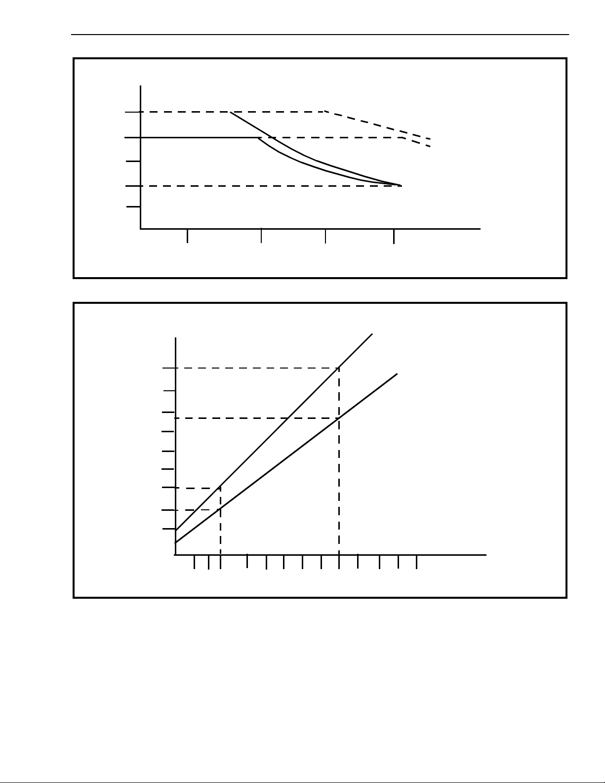
Figure 3a - Loop Current vs.Maximum Loop Current
ILoop = 20mA
Maximum
Loop
Length (Ω)
1800
1600
1400
1200
1000
800
600
400
200
ILoop = 25mA
64
16
20
24
28
32
36
40
44
48
52
56
60
Figure 3b - Maxim um L oop L ength vs Batt ery vo ltag e
VBAT (V)
2-87
Page 6
MH88600 Preliminary Information
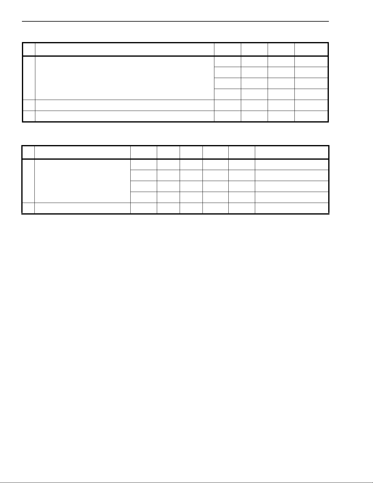
Absolute Maximum Ratings* - Voltages are with respect to AGND.
Parameters Sym Min. Max Un its
1 DC Supply Voltages
(GNDA = GND
Bat
)
2 Storage Temperature T
3 Power Dissipation P
* Exceeding these values ma y cause perm anen t dama ge. Functi onal operati on und er these cond ition s is not implied.
V
DD
V
EE
V
Bat
V
RR
S
D
-0.3 15 V
+0.3 -15 V
+0.3 -80 V
-0.3 40 V
-55 125 °C
Recommended Operating Conditions
Characteristics Sym Min. Typ
1 Operating Supply Voltage V
2 Operating Temperature T
* Typical figures are at 25°C and are for design aid only: not guaran teed an d not subject to producti on testing .
DD
V
EE
V
Bat
V
RR
OP
4.75 5.0 5.25 V
-5.25 -5.0 -4.75 V
-72 -48 -24 V
070°C
*
Max Units Comments
524 V
4W
.
2-88
Page 7
Preliminary Information MH88600
DC Electrical Characteristics †
Paramete rs Sym Min. Typ* M ax Units Test Con dition s
1 Suppl y Current I
I
I
DD
EE
Bat
8.5
5.0
12.0
10.0
4.8
2 Power Consum ption PC 330
755
1556
3 Constant Current
Battery Feed
4 Op erating Loop
Resistance
‡
I
Loop
‡
I
Loop
R
Loop
18
21
2000
20
25
22
30
800
1560
600
5 Off-Hook Detect Threshold SHK
6 GND Button Detect
Threshold
EGB
th
th
10 mA
10 mA
7 Ring GND Over-Current
Protection 32 41 mA
SHK
8
EGB
9 Sink Current
Low Level Output Voltage
&
High Level Output Voltage
Source Current
10
RC
Low Level Input Voltage
High Level Input Voltage
11 High Level Input Current I
12
RD
Sink Current I
13 Clamp Diode Current I
V
14
Internal Reference -7.4 -6.7 -6.0 V LCA linked to V
Ref
V
V
I
I
V
V
OL
OH
OL
OH
IH
IH
RLY
CD
2.4
160
390
IL
4.0
65 mA
0.4 V
0.4 V
1.5 mA VIH = V
65 mA
mA
mA
mA R
mW
mW
mW
mA
mA
Ω
Ω
Ω
Ω
=Open Cct,
Loop
= -48V
V
Bat
Standby
=1200Ω
R
Loop
=0Ω
R
Loop
=-48V
V
Bat
LCA=-5.4V when R
LCA=linked to V
R
=0Ω
Loop
V
=-48V, I
Bat
V
=-48V, I
Bat
V
=-48V, I
Bat
V
=-48V, I
Bat
No Load
V
µΑµΑVOL =0.8V
=-0.2V
V
OH
V
DD
Loop
Loop
LLoop
Loop
Loop
Ref when
=20mA
=20mA
=25mA
=25mA
Ref
-0Ω
* Typical figures are at 25°C and are for design aid only: not guaran teed and no t subject to producti on testing .
† DC Electrical Characteristics are over recommended operating conditions unless otherwise stated.
‡ See Figures 3a and 3b.
2-89
Page 8

MH88600 Preliminary Information
AC Electrical Characteristics† - Voltages are with respect to GNDA unless otherwise stated.
Characteristi cs Sym Min. Typ*Max Units Test Conditions
1 Ringer Voltage VR 105 V
rms
2 Ringer Equivalence No. REN 5
3 Ring Trip Detect Time 200 ms
4 Input Impedance at PG4
at VRX
5 Output Impedance at TX Z
6 Gain 2-Wire to TX: Fixed Gain
Programmable Range
Frequency Response Gain
relative to Gain @ 1kHz
300Hz
600Hz and 2400Hz
3000Hz
3400Hz
7 Gain RX to 2-Wire: Fixed Ga in
Programmable Range
Frequency Response Gain
relative to Gain @ 1kHz
300Hz
600Hz and 2400Hz
3000Hz
3400Hz
Z
RX
112
RRX
TX
3 Ω
A TX +3.5 +4 +4. 5 dB
RTX -12 +6 dB
AR TX
-0.75
-0.1
-0.3
-0.75
0.1
0.1
0.1
0.1
ARX -4. 5 -4 -3.5 dB
RRX -12 +6 dB
ARRX
-0.75
-0.1
-0.3
-0.75
0.1
0.1
0.1
0.1
kΩ See Fig 5
dB
dB
dB
dB
dB
dB
dB
dB
See Fig 6
See Fig 4
Input 1.0V at 1kHz See Fig 5
See Figure 4
Input 1.0V
600Ω 2-Wire Impedance
Input 1.0V at 1kHz See Fig 5
See Figure 4
Input 1.0V
600Ω 2-Wire Impedance
8 2-Wire Return Loss RL 20
18
9 2-Wire Input Impe dance Z
IN
26 dB
dB
10 Transhybrid Loss THL 20 40 dB
11 Longitudi nal Balance 52
41
12 Total Harmonic Distortion
THD
at TX
at 2-Wire
0.1
0.1
1.0
1.0
dB
dB
%
%
Input 1.0V, 200Hz to 3.4kHz
Input 1.0V, 3.4kHz to 4kHz
See Table 1
Input 1.0V at 300Hz to
3400Hz at PG4
40 - 3400Hz
3400-4000Hz
Input 1.0V at 1kHz at 2-Wire
Input 1.0V at 1kHz at PG4
13 Common Mode Reject Ratio CMRR 40 CCITT 0.121
14 Idle Channel Noise at TX
(0dB gain)
Idle Channel Noise at 2-Wire
(0dB gain)
15 Power Supply Reject Ratio V
V
16 Dial Pulse Distortion
V
DD
EE
BAT
Nc
Np
Nc
Np
PSRR 25
20
30
t
d
13
-78
11
-80
18
-73
16
-75
dBrnC
dBrnp
dBrnC
dBrnp
dB
dB
Ripple 1Vpp 1kHz
Measure 2-Wire or TX
dB
0.4 1 ms 2-Wire loop at 1.2kΩ
(SHK High to Low Time)
† AC Electrical Characteristics are over recommended operating unless otherwise stated.
* Typical figures are at 25 C and are for design aid only: not guarantee d and not subject to productio n testi ng.
2-90
Page 9
Preliminary Information MH88600
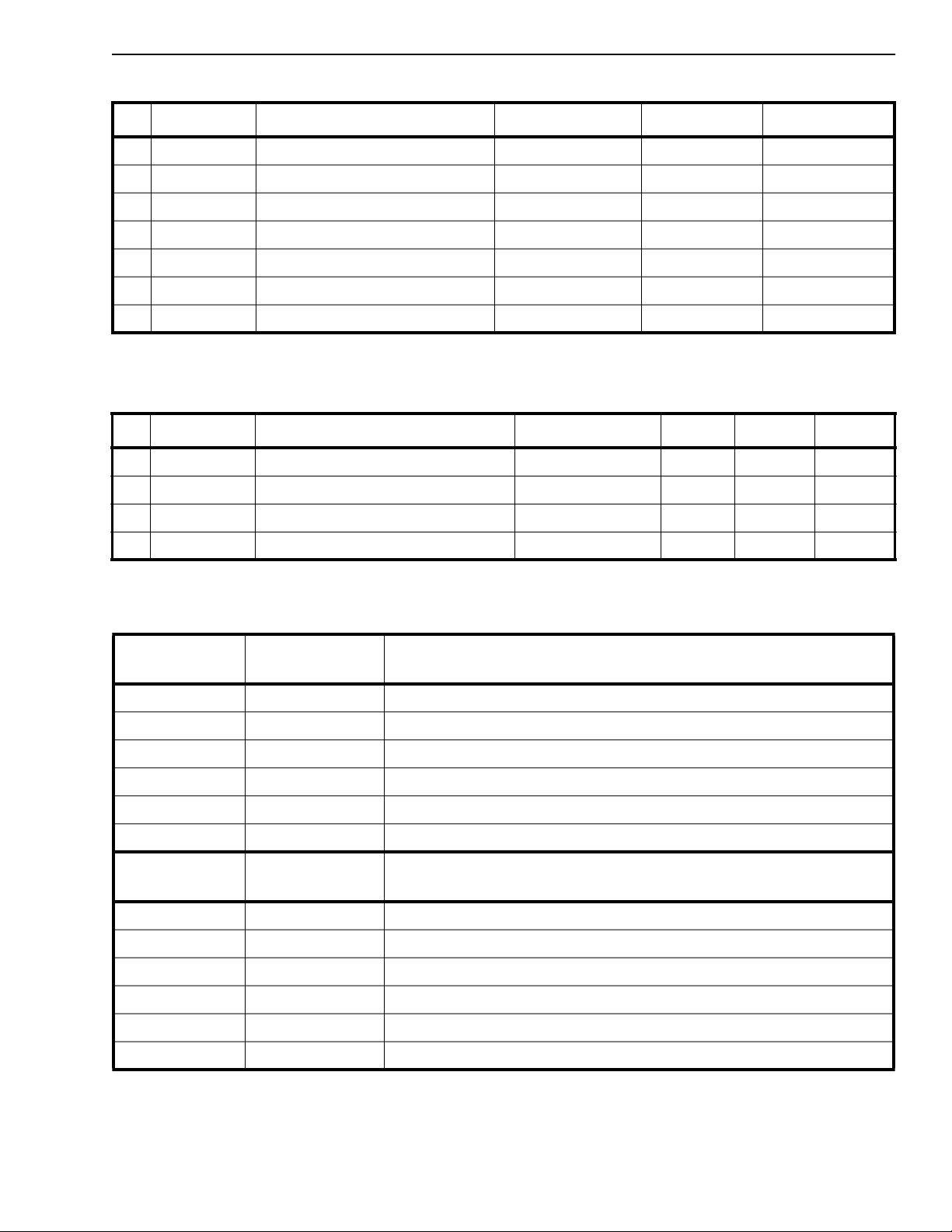
Table 1: Impedance Matching with Jumpers
Zin Code Zin 2-Wire Inpu t Imped ance Administration ZN1 Link to: ZN8 Link to:
1600600Ω --- ZN7 ---
2UK370Ω + 620Ω // 310nF U n ited Kingdom ZN6 ZN13
3D220Ω + 820Ω // 310nF Germany, Austria Z N5 ZN12
4NA350Ω + 1000Ω // 310nF Canada, USA ZN4 ZN11
5F210Ω +880Ω // 310nF France ZN3 ZN10
6N120Ω + 820Ω // 310nF Norway ZN2 ZN9
7A220Ω + 820Ω // 310nF Australia Use D Code Use D Code
Note 1: The above impedances are as suggested by references: BS6305 (UK), REG3 (Australia), Proposed NET4, FCC Part 68 and
recommendations by the various Administrations. Confirm your impedance requirements before proceeding.
Note 2: All links to ZN1 should be as short as possible.
Table 2: Impedance Matching with External Components
Zin Code Zin 2-Wire Input Imp edan ce Ad m inistratio n Rs Rp Cp
1 --- 600Ω + 2.16µF---6kΩ1MΩ 216nF
2 ATT 900 Ω + 2.16µ FAT&T9kΩ1MΩ 216nF
3 NTT 600Ω + 1.0µFNTT6kΩ1MΩ 100nF
4NZ370Ω + (620Ω // 220nF) New Zealand 3.7kΩ 6.2kΩ 22nF
Note 1: The above impedances are as suggested by reference CCITT Q.522. Confi rm your impedan ce require ment s before proce edin g.
Note 2: For Rs, Rp & C calculations, G is set to 10, R is set to 5656.8Ω, refer to figure 8 for additional information.
Table 3: Transmit and Receive Gain Programming
Transmit Gain
(dB)
RTX Resistor
Value (Ω)
Notes
+5.62 270k
+4.0 No Resistor
+3.69 216k
Results in 0dB overall gain when used with Mitel A-law codec (ie MT8965)
Results in 0dB overall gain when used with Mitel µ-law codec (ie MT8964)
+2.1 180k
0.0 141k
-3.0 100k
Transmit Gain
(dB)
RTX Resistor
Value (Ω)
Notes
+6.6 33.1k
+0.0 70.7k
-3.0 100k
-3.69 108k
4.0 No Resistor
Results in 0dB overall gain when used with Mitel A-law codec (ie. MT8964)
Results in 0dB overall gain when used with Mitel µ-law codec (ie MT8965)
-6.5 150k
Note 1: See Figures 4 and 5 for additional details.
Note 2: Overall gain refers to the receive path of PCM to 2-Wire, and to transmit path of 2-Wire to PCM.
2-91
Page 10
MH88600 Preliminary Information
RTX
24
PG1
MH88600
TX
PG3
PG4
25
22
26
V
TX
TRANSMIT
TX
24
PG1
MH88600
GNDA
11
PG2
23
R
RX
V
RECEIVE
RX
RX
Transmit Gain =
Receive Gain =V
Note: PG3 and PG4 pins should be left open circuit. See Table 3.
V
Tx
V
-
TIP
TIP - RING
V
RX
RING
Figure 4 - Configuration of MH88600 for Gain Programming
26
TX
PG3
PG4
25
22
TRANSMIT
V
TX
V
RECEIVE
RX
TX
RX
= RTX (kΩ)x0.007071
70.71
=
R
(kΩ)
RX
2-92
GNDA
11
23
PG2
Transmit Gain =
Rece ive Gain =
Note: PG2 pins should be left open circuit. See Table 3.
V
V
TIP - RING
V
TIP - RING
V
RX
Figure 5 - Configuration of MH88600 for Default Gains
TX
= +4dB
-4dB
=
Page 11
Preliminary Information MH88600
RV1
TO MDF and
SUBSCRIBER SET
RV2
RINGING
GENERATOR
90VRMS
20Hz
K1
~
K1
RELAY
SUPPLY
+ve
K1
14
16
10
15
LCA
20
34
ZN8
MH88600
VDD
VRef
32 27
ZN6
VEE
VBat
21213
ZN1
PG3
EGB
SHK
GNDA
TX
PG4
811
25
26
22
19
18
Bat
GND
VX
CODEC
VR
39
ZN13
TF1
9
TF2
6
TIP
5
RING
4
RF2
3
RF1
RD
VRR
RC
17
RINGING
CONTROL
C1
+5V-5V
C2
RV1,RV2 - V150LA 150Vrms
C1,C2 - 10µ F/10V Electrolytic or Tantalum
K1 - Relay E/M, 12V, 1Form C
Figure 6- Ty pical Application Circuit
13J (10/1000)
2-93
Page 12
MH88600 Preliminary Information
RINGING
GENERATOR
45 V
RMS
20Hz
+-
~
RV1
TO MDF and
SUBSCRIBER SET
RV2
45V
RMS
20Hz
~
K1
30k
0.15W
K1
+ve
RELAY
SUPPLY
9
10
6
5
4
3
16
K1
14
15
39 34
ZN13
TF1
TF2
TIP
RING
RF2
RF1
RD
VRR
RC
VRef
LCA
20
17
ZN8
MH88600
VEE
VDD
1213
32
ZN6
27
ZN1
25
PG3
26
TX
22
PG4
19
EGB
18
SHK
Bat
GND
GNDA
VBat
8112
-48V
RINGING
CONTROL
C1
+5V-5V
Figure 7 - Application Circuit for Balanced Ringing
C2
2-94
Page 13
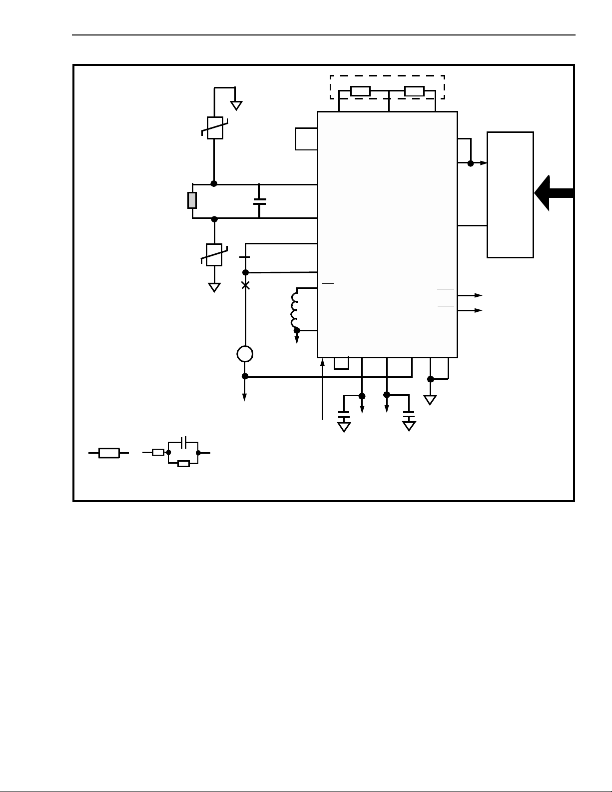
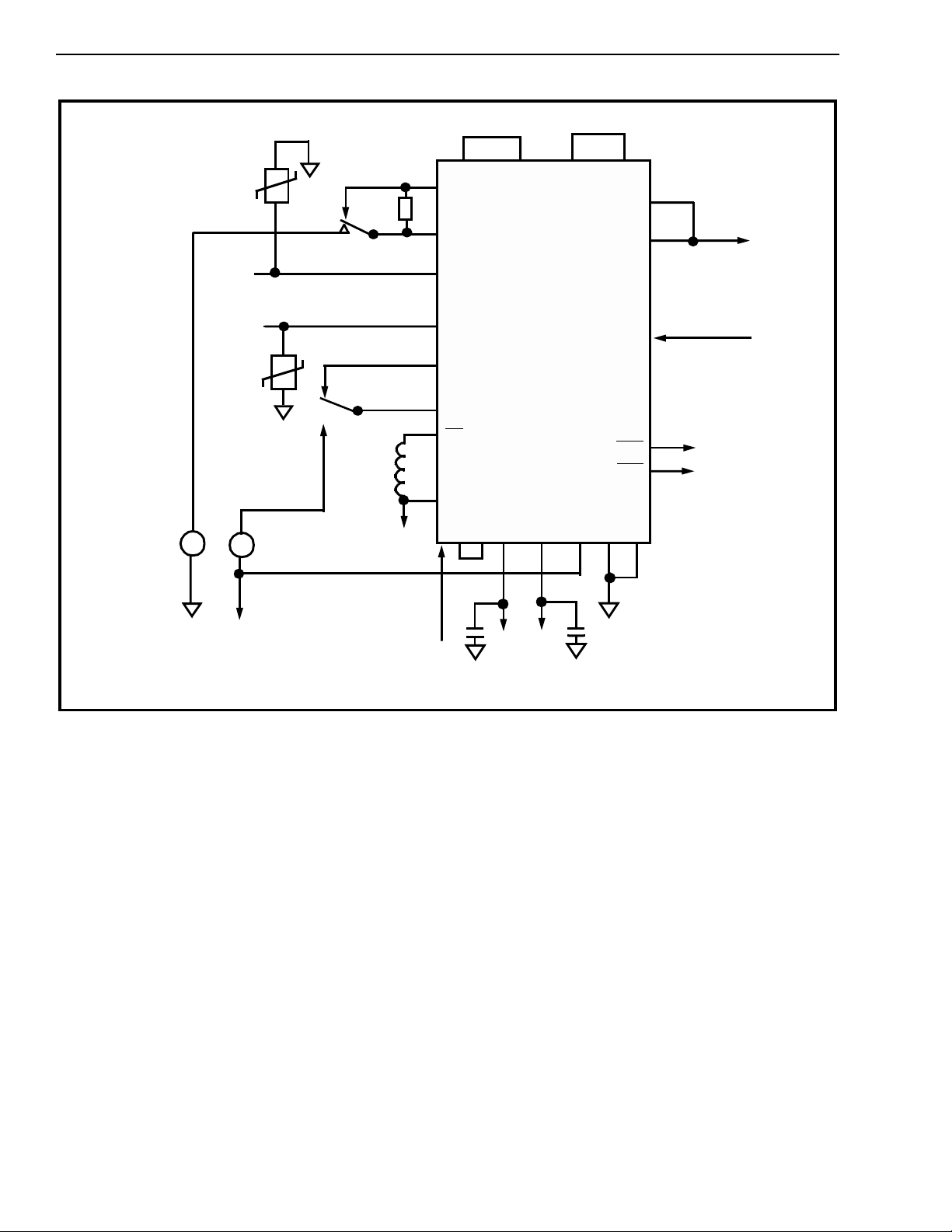
Preliminary Information MH88600
C1=C2=10µF, 10V Electrolytic
or tantalum
C3=1nF, 250V, 20%
C3 is recommended to
improve stability when
used on loop lengths less
than 500Ω total or used
with active loads
Z=G x Zo
R=565.68 x G Ω
G may be chosen to
suit preferred component
values (useful for
capacitive elemen ts);
resistive elements should
have values in the range
of 1k to 1MΩ. Typical values
are G = 10
See Tab le 2 for external
network examples.
Set Rp=1MΩ for networks
not specifying an Rp
RV1
Zo
RV2
RINGING
GENERATOR
90VRMS
20Hz
~
K1
K1
RELA Y
SUPPLY
C3
+ve
K1
16
14
10
3
9
6
5
4
15
40
ZN13
TF1
TF2
TIP
RING
RF2
RF1
RD
VRR
RC
17
External Network
Z
ZN8
MH88600
VDD
VRef
LCA
20
27
VEE
ZN6
21213
R
21
ZN1
25
PG3
26
TX
22
PG4
19
EGB
18
SHK
Bat
VBat
GNDA
GND
811
VX
CODEC
VR
RINGING
CONTROL
Z
Rs
=
Cp
Rp
C1
+5V-5V
C2
Figure 8 - Using an External Network to Match any Zo
2-95
Page 14
MH88600 Preliminary Information
AAAA
AAAA
AAAA
AAAA
A
A
AAA
AAAA
AAAA
AAAA
AAAA
AAAA
AAAA
AAAA
AAAA
AAAA
AAAA
AAAA
AAAA
AAAA
AAAA
AAAA
AAAA
AAAA
AAAA
AAAA
AAAA
AAAA
AAAA
2.0
(50.8)
AAA
AAAA
AAAA
AAAA
AAAA
AAA
AAAA
AAAA
AAAA
AAAA
AA
AA
0.3
(7.62)
MH88600
Note 1
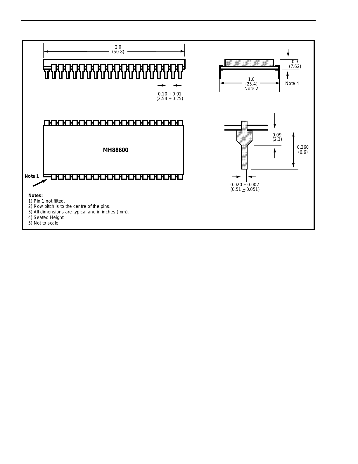
Notes:
1) Pin 1 not fitted.
2) Row pitch is to the centre of the pins.
3) All dimensions are typical and in inches (mm).
4) Seated Height
5) Not to scale
0.01
0.10 +
(2.54 + 0.25)
Figure 9 - Mechanical Data
1.0
(25.4)
Note 2
0.020 +
0.002
(0.51 + 0.0 51 )
0.09
(2.3)
Note 4
0.260
(6.6)
2-96
 Loading...