

Page 1
MH88615
ONS Subscriber Line Interface Circuit
Advance Information
Features
• ONS SLIC
•Variants
- 1 Germany
-3 UK
- 7 North America
• Transformerless 2W to 4W conversion
• Battery Feed to line
• Off-Hook and dial pulse detection
• Tip and Ring gro und ov er-cur rent p rotec tion
• Power Denia l
• Integral Ringing A m p li fier
• Programmable Loop Current
•Wide V
Operatin g Range
BAT
Applications
Line Interfac e for
• PABX
•Pair Gain Systems
• Satellite Co mm unicati on Sys tem s
• Key Telephone S ystem s
• Marine Syst em s
• Cordles s Loc al Loo p
ISSUE 1 April 1995
Ordering Information
MH88615-1 20 Pin SIL Package
MH88615-3 20 Pin SIL Package
MH88615-7 20 Pin SIL Package
0°C to 70°C
Descript io n
The Mitel MH88615 ONS SLIC provides a complete
interface between a switching system and a
subscriber loop. The functions provided by the
MH88615 include battery feed and integral ringing
amplifier feed to the subscriber line, 2W to 4W
conversion current feed, off-hook and dial pulse
detection. The device is fabricated as a thick film
hybrid in a 20 pin single-in-line package.
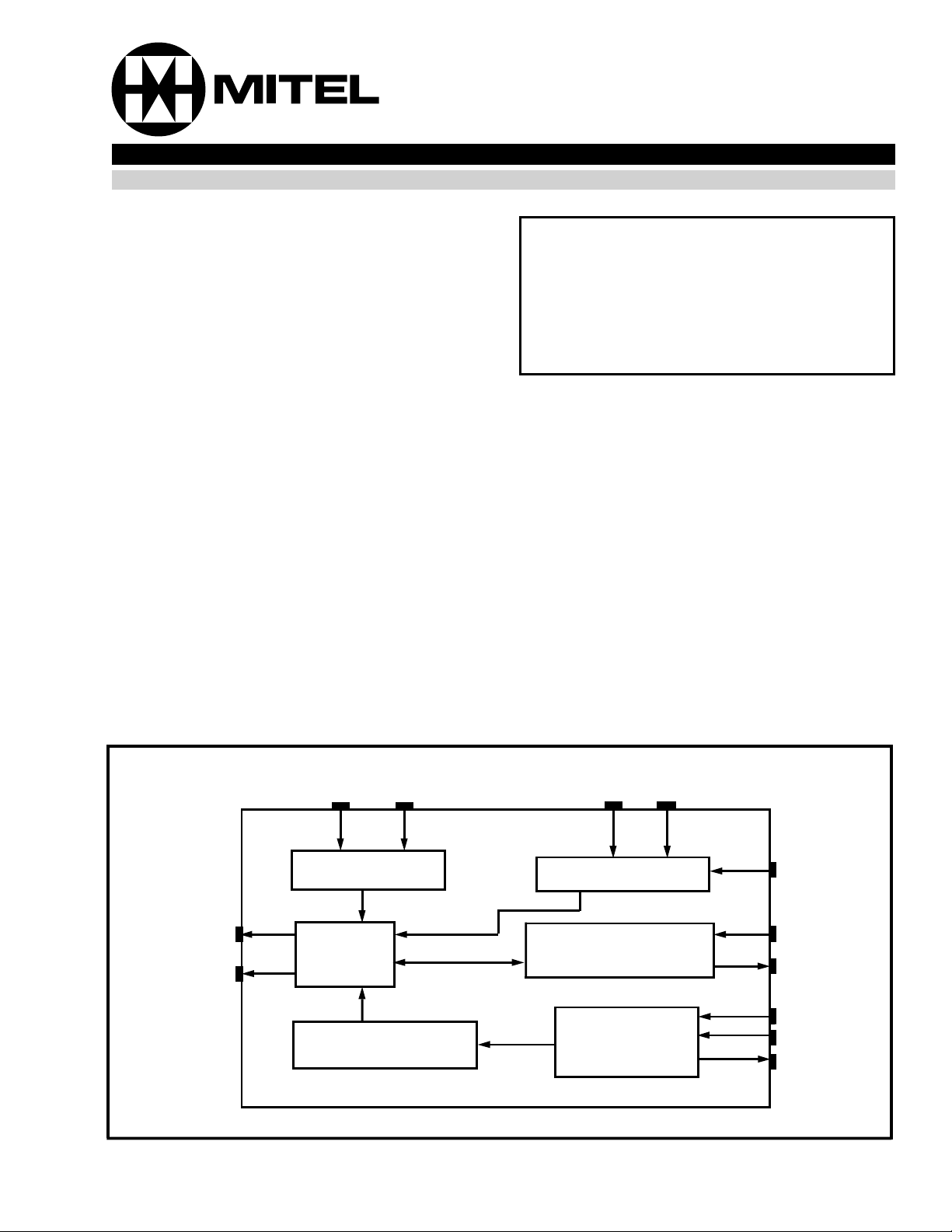
TIP
RING
PD
Power Denial
Tip &
Ring
Drivers
Current Feed
VBat
Constant
2-Wire to 4-W ire
Figure 1 - Block Diagram
DCRI
Ringing Control
Conversion
Loop
Supervision
RV
RC
VR
VX
VRef
CAP
SHK
2-139
Page 2
MH88615 Advance Information
TIP
RING
NC
DCRI
LPGND
VBat
NC
VDD
AGND
VEE
RC
PD
NC
SHK
VR
VRef
CAP
VX
NC
RV
1
2
3
4
5
6
7
8
9
10
11
12
13
14
15
16
17
18
19
20
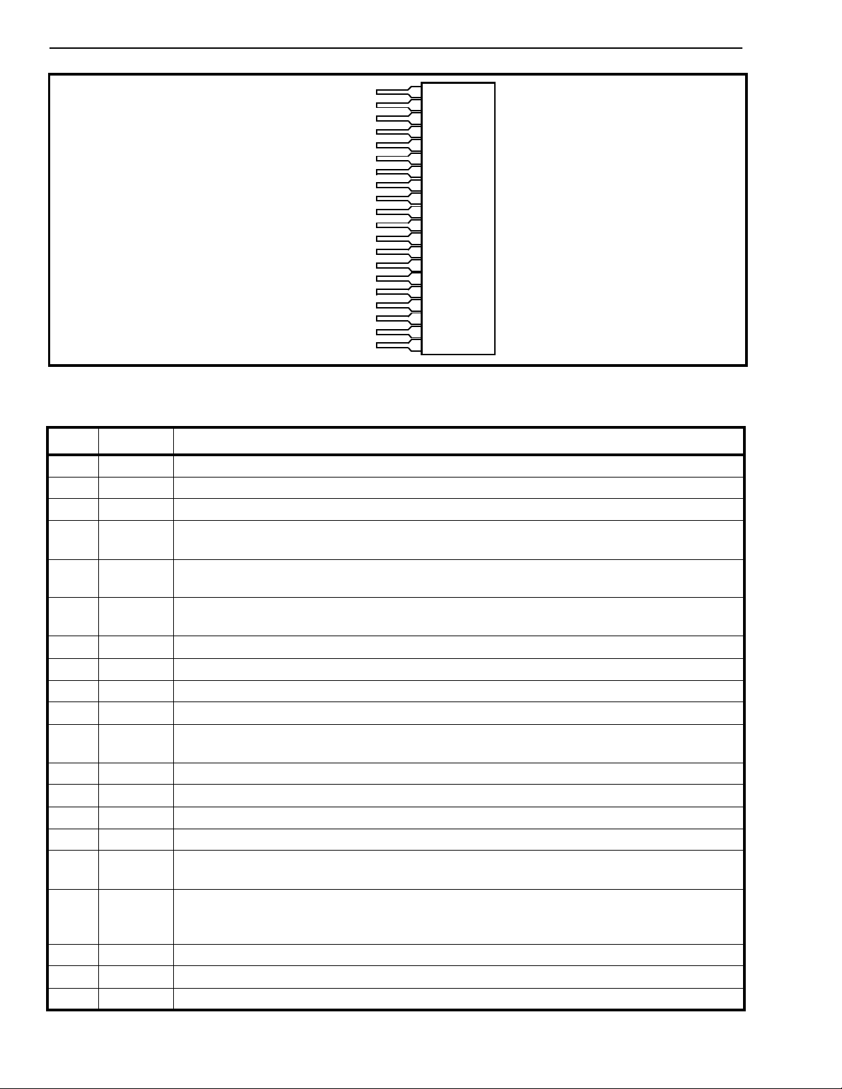
Figure 2 - Pin Description
Pin Description
Pin # Name Description
1TIPTi p Le a d. Connects to the “Tip” lead of subscriber line.
2 RING Ring Lead. Connects to the “Ring” lead of subsriber line.
3NCNo Con necti on. This pin may be use d for internal connecti o ns.
4 DCRI DC Ringing Voltage Input. A continuous 120 Vd c is applied to th is pin. This voltage is the
positive supply rail for the internal ringing am plif ier for subscriber line.
5LPGNDBattery Ground. V
dumping ground.
6 VBat Battery Voltage. Battery supply feed for subscriber line. Typically -48Vdc is applied to this
pin.
7NCNo Con necti on. This pin may be use d for internal connecti o ns.
8VDDPositive Supply Voltage. +5V dc supply rail.
9AGNDAnalogue Ground. V
10 VEE Negati ve Supp ly Voltage. -5V dc supply rail.
11 RC Ringing Control. This input enables the ringing voltage fe ed to Tip and Ring for subscriber
line.
12 PD Power Denial. A logic high will isolat e the batte ry voltage for Tip and Ring.
13 NC No Connecti on . This pin may be used for intern al connecti on s.
14 SHK Switch Hook Detect. A logic high indicates when subscriber line has gone off-hook.
15 VR Receive Signal. This is the 4 wire analogue signal received at subscriber ’ s set.
16 VRef Reference Voltage. A dc reference voltage is applied to this pin to set the constant current
feed to subscriber line. This pin may also be grounded for normal 25mA loop current.
17 CAP Ring Trip Filter Capacitor. A capacitor is normally connected from this pin to ground and
filters out low frequency ringing signals, preventing false off-hook conditions.
return path for subscriber line. Connects to the systems’s energy
Bat
and VEE return path.
DD
18 VX Transmit Signal. This is the 4 wire analogue signal transmit ted from subscriber ’s set.
19 NC No Connecti on . This pin may be used for intern al connecti on s.
20 RV Ringing Voltage. 1. 5 Vrms signal is injected to this pin.
2-140
Page 3

Advance Information MH88615
Functional Description
The Mitel MH88615 ONS SLIC provides a complete
interface between a switching system and a
subscriber loop. The functions provided by the
MH88615 include battery feed and integral ringing
amplifier feed to the subscriber line, 2W to 4W
conversion, constant current feed, off-hook and dial
pulse detection. The device is fabricated as a thick
film hybrid in a 20 pin single-in-line package.
The MH88615 is intended for applications where low
cost and basic functionality is important. The
MH88615 features an integral ringing amplifier which
enables a system designer to provide typically 60
Vrms ringing without having to generate a high
voltage, high current ac signal.
The SLIC uses a transformerless 2-4 wire converter
which can be connected to a CODEC to interface the
2 wire subscriber loop to a TDM (time division
multiplex) PCM (pulse code modulation) digital link.
Powering of the subscriber line is provided though
precision battery feed resistors on the hybrid. The
thick film hybrid circuit also contains control,
signalling and status circuits which combine to
provide a complete functional solution. A power
denial facility is provided which isolates the Battery
Feed from Tip and Ring.
The MH88615 is designed to meet German
regulatory approvals, UK regulatory approvals
(BS6305), and capable of meeting the approvals for
the USA ( FCC Part 68/EIA 464).
Powe r D e n i a l
A logic high voltage applied to the power denial input
effectively removes the battery voltage from the loop
driver circuitry. The resulting loop current is
negligible and power consumption is minimise d. The
power denial function is useful for disabling a loop
which may have a ground fault.
The SLIC is capable of detecting and indicating offhook and unbalanced conditions as well as inhibiting
ringing while in power denial.
Input and Network Impedanc e
The Input and Network Balance Impedances are
defined by the variant type on the MH88615.
MH88615 -1Germa ny
= 220Ω + (820Ω//115nF)
Z
in
Z
= 220Ω +(820Ω//115nF)
net
MH88615-3 UK
Z
= 370Ω + (620Ω//310nF)
in
Z
= 300Ω + (1000Ω//220nF)
net
MH88615-7 North Ame rica
= 600Ω
Z
in
Z
= 350Ω (1kΩ//210nF)
net
Ringing Amplifier
Constant Current Feed
The loop current is programmed by the dc reference
voltage applied to V
Ref
.
Switch Ho ok Det ecti on
When the dc current exceeds an internal threshold
level, the switch hook output (SHK) will go high. If
the loop resistance is so high that V
supply the required loop current, the output SHK will
go low. This indicates that the loop resistance is too
high and the line is on hook.
can no longer
Bat
DC Loop Current Limit
Under Tip or Ring ground conditions the loop current
is nominally limited to 42mA.
The MH88615 incorporates an integral ringing
ampl ifier. A n omin al 1. 5Vrms ac signa l is a pplied to
the RV pin and this produces a ringing signal of
typically 60 Vrms. This should ensure that the SLIC
can support a REN of 5.
Transmit Gain
Transmit gain (Tip-Ring to Vx) is fixed at 0.dB. A
dcbias on the ac input signal does not effect the
ringing signal.
Receive G ain
Receive G ain ( V R to T IP - RING) is fix ed a t 0dB.
For correct gain, the SLIC input impedance must
match the line impedance
2-141
Page 4

MH88615 Advance Information
Absolute Maximum Ratings*- Voltages are with respect to AGND.
Parameter Symbol Min Max Units Commen ts
1 Supply Voltages V
2 Storage Temperature T
* Exceeding these values ma y cause perm anen t dama ge. Functi onal operati on und er these cond ition s is not implied.
V
Bat
V
V
DCRI
DD
EE
S
0.3
-0.3
0.3
-0.3
65
6
-6
140
-55 125 °C
V
With respect LPGND
V
V
V
With respect LPGND
Recommended Operating Conditions
Characteristics Sym Min Typ* Max Units Com men ts
1 Supply Voltages V
V
2 Operating Temperature T
Bat
V
DD
V
DCRI
OP
EE
-20
4.75
-4.75
0
-48
5.0
-5.0
48
-60
5.25
-5.25
130
V
V
V
V
02070°C
3 AC Ring Generator
Voltage
Frequency
* Typical figures are at 25°C with nominal +5V supplied and are for design aid only .
V
F
R
R
17
60 90
68
V
RMS
Hz
DC Electrical Characteristics*
Characteristics Sym Min Typ Max Units Test Comments
1
Supply Current
I
I
I
DD
EE
Bat
10
5
2.5
mA
mA
mA PD on
V
BAT
= -48V
2
Power Consumption PC 150
3
Constant Current Line Feed
4
Adjustable Loop Current Range
5
Maximum Operati ng Loop
Resistance
6
Ring Ground Over-Current 42 mA
7
Off-Hook Detect
Output Low Voltage
Output High Voltage
8
Off-Hook Detect
Output Low Current
Output High Current
9
RC, PD Control Input
Input Low Voltage
Input High Voltage
10
RC, PD Control Input
Input Low Current
Input High Voltage
* -48V and are for desig n aid onl y
I
I
R
V
Loop
Loop
Loop
V
OL
V
OH
I
OL
I
OH
V
OL
OH
I
IL
I
IH
mWmWStandyb y
1700
23 25 27
mA
Active
V
= AGND
Ref
18 30 mA
1200 Ω V
I
Loop
R
Bat
Loop
=-48V @
=18mA,
=includes
telephone set
Active High Logic
0.4 V
2.7
4
-400
V
mA
µA
Active High Logic
0.7 V
2.0
-500
500
V
µA
µA
2-142
Page 5
Advance Information MH88615
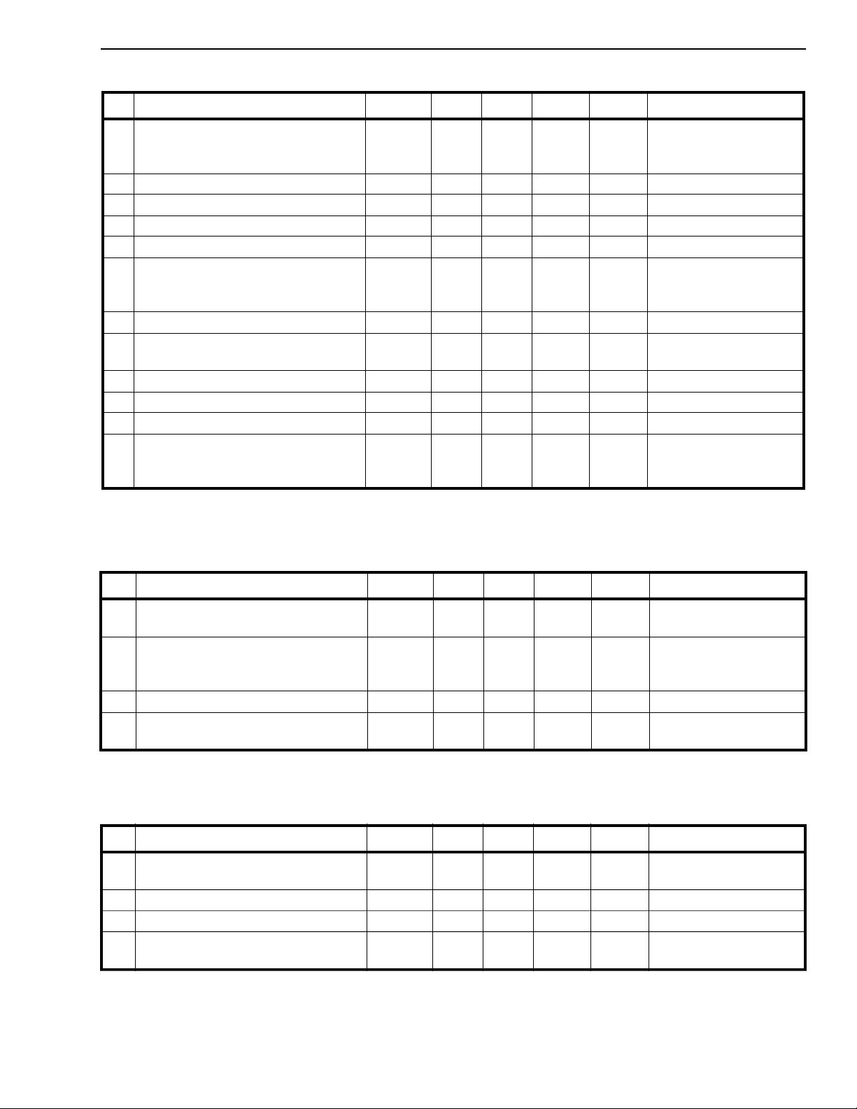
AC Electrical Characteristics*
38
‡
Max Units Test Comments
VrmsHzSuperimposed on
68
V
= -48V. RV=1.5
Bat
Vrms
kΩ
300Hz to 3.4 kHz
300 Hz to 3.4 kHz
1kHz @
VDD
Characteristics Sym Min Typ
1
Ringing voltage V
2
Ring Trip Detect Time 100 ms
3
Input Impedance at VR 47 100
4
Output Impe dance at Vx 10 Ω
5
Gain 2-wire to Vx -0.25 0 0.25 dB
6
Frequency Response 2-wire to Vx -0.15 0 0.1 5 dB Relative to 1kHz
7
Gain Vr to 2-wire -0.25 0 0.25 dB
8
Frequency Response Vr to 2-wire -0.15 0 0.15 dB Relative to 1kHz
9
Total Harmonic Distortion THD 0.5 %
10
Common M ode Reject ion Rat io CMRR 50 dB
11
Idle Channel Noise Nc 12 dBrnC
12
Power Supply Rejection Ratio at 2-
R
F
R
17
PSRR 25 dB Ripple 0.1V
Wire or VX
* Exceeding these values ma y cause perm anen t dama ge. Functi onal operati on und er these cond ition s is not implied.
‡ Typical figures are at 25°C and a re for desi gn aid only.
Note 1: All of the above test condition s use a test source impedance which ma tche s the device’s impedan ce.
Note 2: THD is mea sured with “A Weight” fil ter.
AC Electrical Characteristics*- MH88615-1
Characteristics Sym Min Typ Max Units Test Comments
1
Ringer Equivalence REN 5 1 REN= 8000Ω
@ 25 Hz
2
Return Loss RL 20
24
20
3
Transhybrid Loss
4
Longitudinal to
Metallic Balance
* Exceeding these values ma y cause perm anen t dama ge. Functi onal operati on und er these cond ition s is not implied.
Note: Return Los s refere nce im peda nce are def ined by varian t type.
Transhybrid Loss is measured when terminated with network impedance.
THL
24
32
54
dB
dB
dB
dB
dB
dB
200 Hz - 500 Hz
500 Hz - 2.5 kH z
2.5kHz - 3.4 kH z
300 Hz - 3.4 kHz
50 Hz - 300 Hz
300 Hz - 4 kHz
AC Electrical Characteristics*- MH88615-3
Characteristi cs Sym Min Typ Max Units Test Comments
1
Ringer Equivalence REN 4 4 REN= 2200Ω
@ 25 Hz
2
Return Loss RL 20 dB 300 H z - 3 . 4 k H z
3
Transhybrid Loss THL 20
4
Longitudinal to
52 dB 300 Hz - 3.4 kHz
Metallic Balance
* Exceeding these values ma y cause perm anen t dama ge. Functi onal operati on und er these cond ition s is not implied.
Note: Return Los s refere nce im peda nce are def ined by varian t type.
Transhybrid Loss is measured when terminated with network impedance.
dB
300 Hz - 3.4 kHz
2-143
Page 6
MH88615 Advance Information
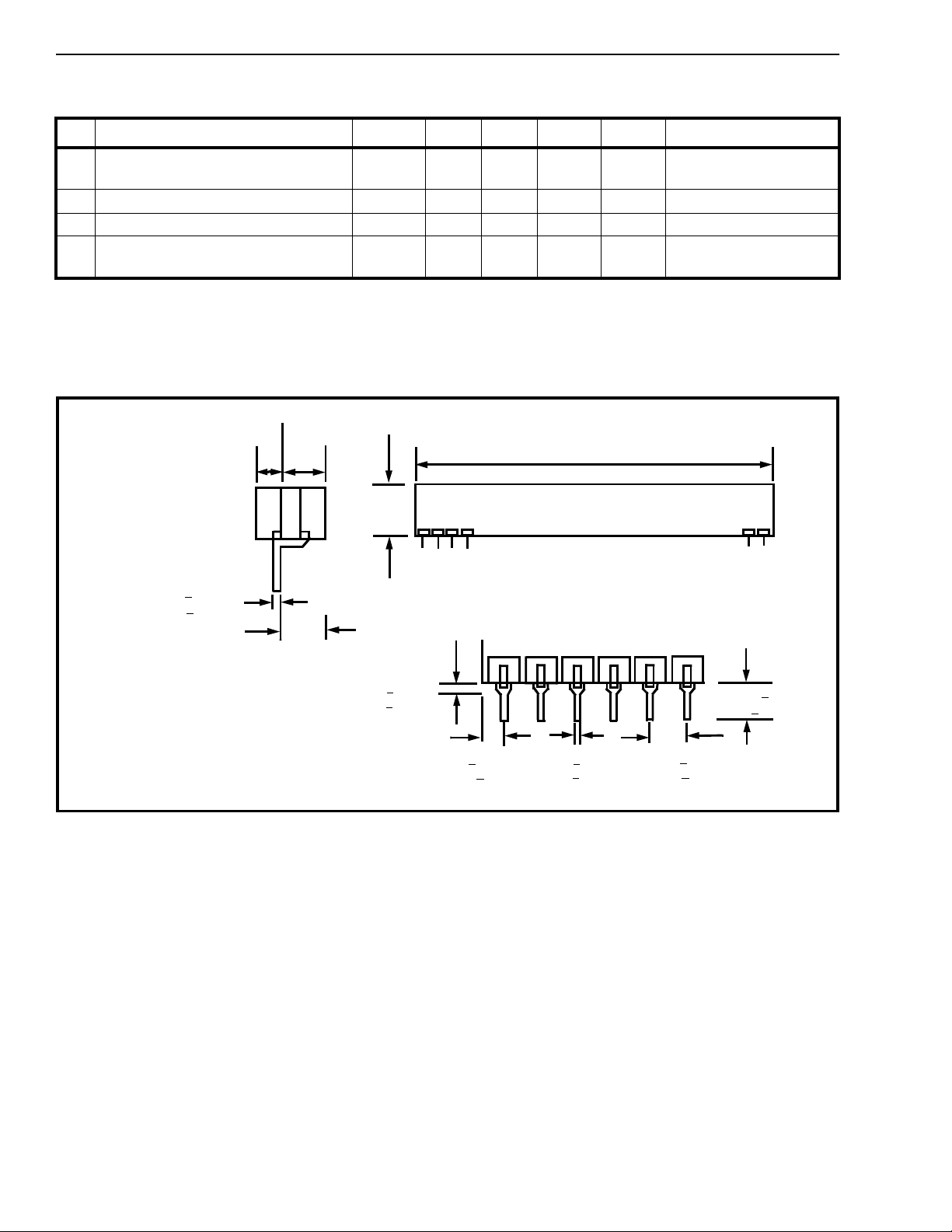
AC Electrical Characteristics*- MH88615-7
Characteristics Sym Min Typ Max Units Test Comments
1
Ringer Equivalence RE N 5 1 REN= 5000Ω
@ 30 Hz
2
Return Loss RL 24 dB 300 Hz - 3 .4 kH z
3
Transhybrid Loss THL 20
4
Longitudinal to
52 dB 300 Hz - 3.4 kHz
Metallic Balance
* Exceeding these values ma y cause perm anen t dama ge. Functi onal operati on und er these cond ition s is not implied.
Note: Return Los s refere nce im peda nce are define d by varian t type.
Transhybrid Loss is measured when terminated with network impedance.
dB
300 Hz - 3.4 kHz
Side View
0.010 +
(0.25 +
Notes:
1) Not to scale
2) Dimensions in inches).
3) (Dimensions in millimetres).
*Dimen sions to centre o f pin &
tolerance non accumulative.
0.25 Ma x
(6.4 Max)
0.00 5
0.13)
0.29 Max
(7.4 Max)
0.12 Max
0.750 Max.
(19.0 Max.)
0.05 +
(1.3 +
0.02
0.5)
12
*
3
0.05 +
(1.25 +
4
0.020
0.5)
Figure 3 - Mechani cal Data
2.1 Max. (106.7 Max.)
0.020 +
0.005
(0.5 + 0.13)
0.100 +
(2.54 +
*
0.01 0
0.25)
19
0.18 0 +
(4.6 +
20
0.02
0.5)
2-144
 Loading...