

Page 1
MH89793
E1Transceiver with Selectable Impedance
Preliminary Info rmatio n
Features
• Complet e primary ra te 20 48kb /s CEPT line
driver and re ceiver
• Onboard pul se tran sform ers for transm it and
receive
• Meets lates t E T S I req uirements [ET S I ETS 300
011 (NET 5)]
• Inductorless clock recovery
• Loss of signal (LOS
) indication
• Single +5 V ope ration
• Compatible with MT9079 Fra mer
• Selectable termin atio n imped anc e
Applications
• Primary rate ISDN network Interface
• Multiplexe r equ ipm ent
• Private Network links
• Isochrono us LA NS/WANS
ISSUE 1 April 1995
Ordering Information
MH89793 28 Pin DIL P ackage
Surface Mount Option is available by adding
the suffix “S”
0°C to +70°C
Description
The Mitel MH89793 is a low cost E1 line
driver/receiver with clock extraction requiring no
external components.
The device is suitable for both 120R and 75R
applications, by linking external pins.
By combining the MH89793 with Mitel’s E1 framer,
the MT9079, a cost effective and efficient interface to
E1 lines can be built.
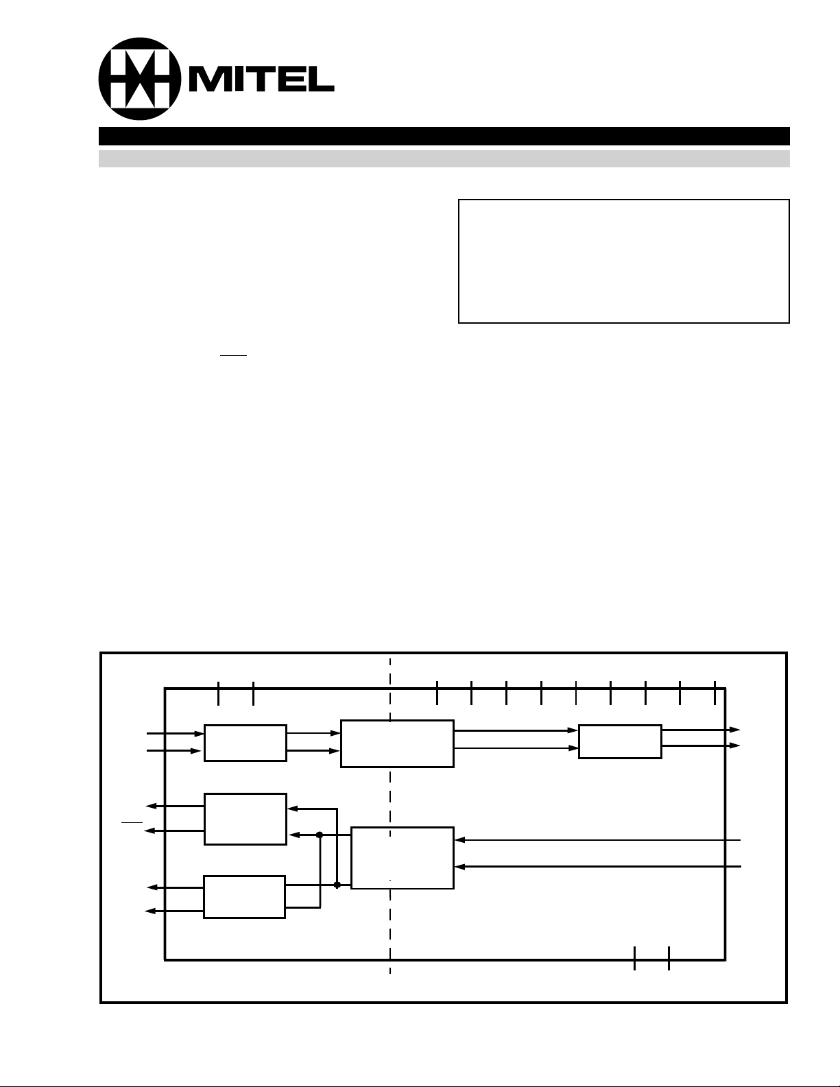
TxA
TxB
E2o
LOS
RxA
RxB
VDD
Recovery
Receiver
VSS
Line
Driver
Clock
Line
EQUIPMENT SIDE
TZA1 TZA2 TZA3 TZC2 TZD2TZB1 TZD1TZB2 TZC1
Transmit
Isolation
Transformer
Receive
Isolation
Transformer
LINE SIDE
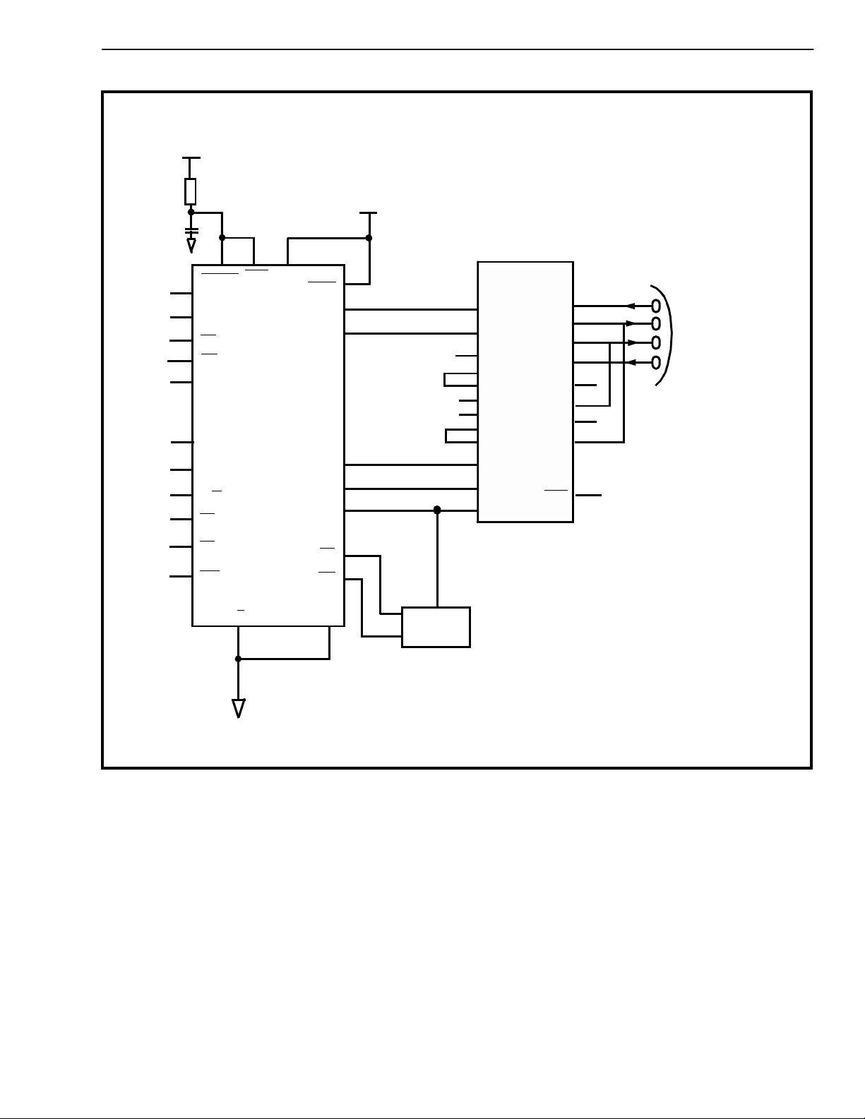
Figure 1 - Functional Blo ck Diag ram
6dB
Pad
RZA RZB
TLA
TLB
RLA
RLB
4-229
Page 2
MH89793 Preliminary Information
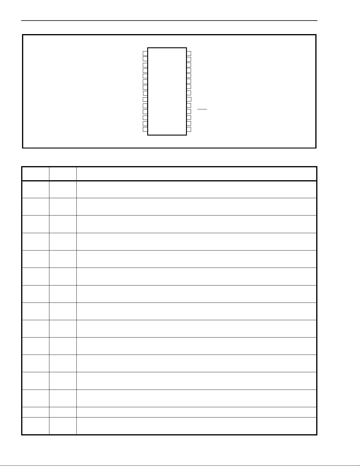
RLA
RLB
TLA
TLB
TZD2
TZC2
TZA3
TZB1
TZA2
TZB2
TZD1
TZC1
TZA1
NC
1
2
3
4
5
6
7
8
9
10
11
12
13
14
15
16
17
18
19
20
21
22
23
24
26
28
25
27
TXA
TXB
NC
NC
NC
VDD
E20
RXB
RXA
VSS
LOS
NC
RZA
RZB
Figure 2 - Pin Connections
Pin Description
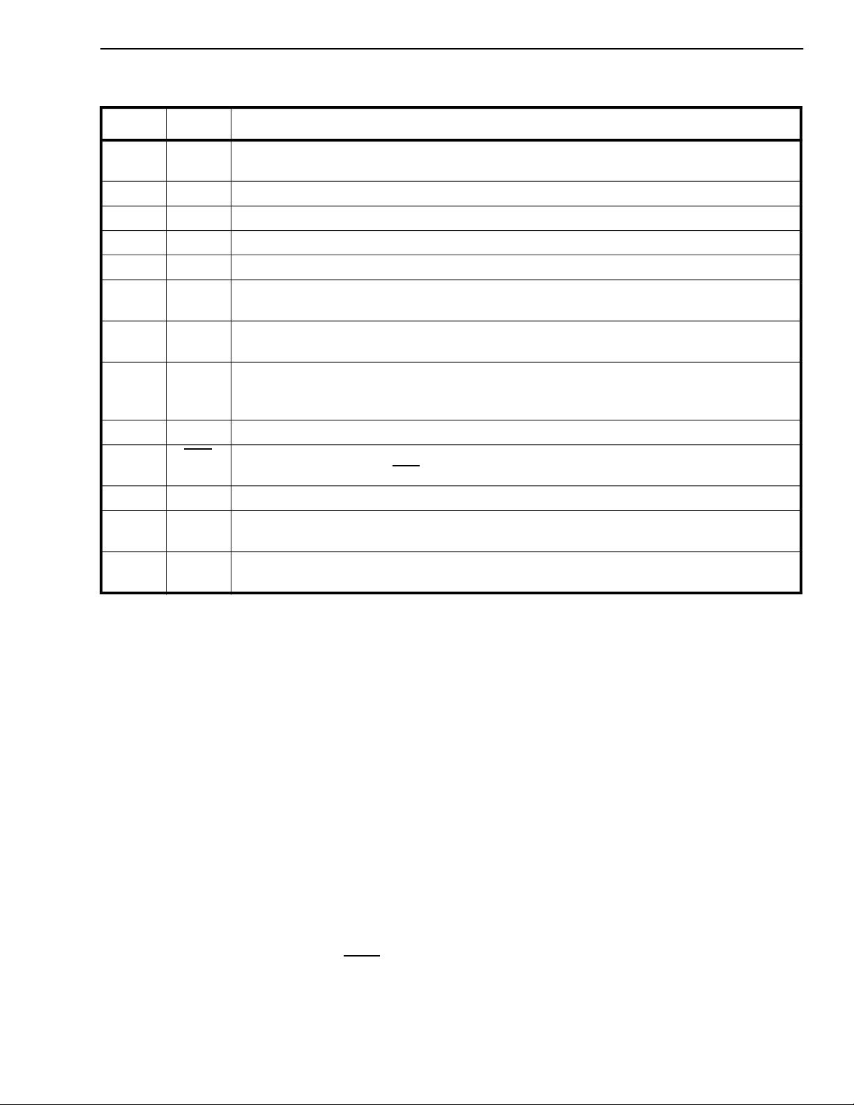
Pin # Name Description
1RLAReceived Li ne A (Inp ut). The A wire or Tip connection of the E1 receive line is connected
to this pin .
2RLBReceived Line B (In put). The B wire or Ring connection of the E1 receive line is
connected to this pin.
3TLATransmit Line B (Output). The A wire or Tip connection of the E1 receive line connected
to this pin .
4TLBTransmit Line B (Output). The B wire or Ring connection of the E1 receive line connected
to this pin .
5TZD2Transmit Impedance Select. This pin is connected to pin 4 TLB to select 75Ω impedance.
For 120Ω operation this pin is left ope n circuit.
6TZC2Transmit Impedance Select. This pin is connected to pin 3 TLA to select 75Ω impedance.
For 120Ω operation this pin is left ope n circuit.
7TZA3Transmit Impedance Select. This pin is connected to pin 9 TZA2 to select 75Ω
impedance. For 120Ω operation this pin is left open circuit.
8TZA3Transmit Impedance Select. This pin is connected to pin 10 TZB2 to select 120Ω
impedance. For 75Ω operation this pin is left open circuit.
9TZA2Transmit Impedance Select. This pin is connected to pin 7 TZA3 to select 75Ω
impedance. For 120Ω operation this pin is left open circuit.
10 TZB2 Transmit Impedance Select. This pin is connected to pin 8 TZB1 to select 120Ω
impedance. For 75Ω operation this pin is left open circuit.
11 TZD1 Transmit Impedance Select. This pin is connected to pin 4 TLB to select 120Ω
impedance. For 75Ω operation this pin is left open circuit.
12 TZC1 Transmit Impedance Select. This pin is connected to pin 3 TLA to select 120Ω
impedance. For 75Ω operation this pin is left open circuit.
13 TZA1 Transmit Impedance Select. This pin is connected to pin 9 TZA2 to select 120Ω
impedance. For 75Ω operation this pin is left open circuit.
14 NC No Connection. This pin is used for internal connection.
15 TXA Transmit A (Input). A unipolar signal from the framer device used in conjunction with TXB
is used to generate the bipolar output signal.
4-230
Page 3
Preliminary Information MH89793
Pin Description (Continued)
Pin # Name Des crip tio n
16 TXB Transmit B (Input). A unipolar signal from the framer device used in conjunction with TXA
is used to generate the bipolar output signal.
17 NC No Connection. This pin is used for internal connection.
18 NC No Connection. This pin is used for internal connection.
19 NC No Connection. This pin is used for internal connection.
20 VDD D.C. Power (Input). +5V supply.
21 E2o 2 048kHz Ex tractio n Clock (Ou tput). This clock is extracted by the device from the
received signal. It is used internally to clock in data received from RLA and RLB.
22 RXB Receive B (Output). This pin is connected to the negative receive pin of the framer and
provides a signal of the same form at as RXA.
23 RXA Receiver A (Outpu t ). The bipolar CEPT signal received by the device at RLA and RLB
input is converted to a unipolar format and output at this pin. This pin is connected to the
positive receive pin of the framer.
24 VSS Ground (Input). D.C. power retu rn path.
25 LOS
Loss of Signal (Output). This pin goes low when 128 contiguous zeros are received on
the RLA and RLB inputs. LOS
is reset when 64 ones are received in dual E1 frame periods.
26 NC No Connection. This pin is used for internal connection.
27 RZA Receive Impedance Select. This pin is connected to pin 17 RZB to select 75Ω input
impedance. For 120Ω operation this pin is lef t ope n circuit .
28 RZB Receive Impedance Select. This pin is connected to pin 16 RZA to select 75Ω input
impedance. For 120Ω operation this pin is lef t ope n circuit .
Functional Description
The MH89793 is an E1 digital trunk interface which
when used with an approved framer will conform to
CCITT recommendation G.703 for PCM30 and I.431
for the ISDN. The functions provided include line
driver and receiver circuitry, inductorless clock
recovery, and loss of signal indication.
Bipolar Line Transmitter
The MH89793 transmitter interfaces to the
transmission line through an internal pulse
transformer which combines the TxA and TxB data
into an AMI line coded signal. This is then passed
through the 6dB pad prior to being applied to the
line.
Bipolar Line Receiver
Clock Extractor
The MH89793 receiver inter faces to the trans miss ion
line through an internal pulse transformer which
splits the received AMI lines signal into RxA and
RxB. The line impedance is selected by linking
appropriate option pins.
Attenuation of the transmission line shall not exceed
6dB (at 1024kHz) and attenuation characteristics
shall be close to the “square root of f”.
The MH89793 contains a clock extraction circuit that
generates the E2o clock from the received data
without the use of external crystals or a tunable
inductor.
The edge of the E2o extracted clock approximately
aligns with the centre of the received data pulse.
Af (dB) = AF
Where:
(dB)* √f
ref
f
ref
AF - attenuation at frequency f in dB
- attenuation at frequency f
AF
ref
f
- reference frequency (in this case 1024) kHz
ref
in dB (in kHz)
ref
f - frequenc y i n k H z
4-231
Page 4
MH89793 Preliminary Information
Loss of Signal
The circuitry on board the hybrid is capable of
detecting 128 continuous ZEROs received on RLA
and RLB and indicating this condition as a logic low
on pin 9, (LOS)
received in a two E1 frame period.
. LOS will not reset until 64 ONEs are
VDD
10K
0.1µ
33
31
26
32
8-15
18-22
23
24
25
2
7
1
RESET
DSTi
DSTo
F0i
C4i
E8Ko
D0-7
AC0-4
R/W
CS
DS
IRQ
TAIS V
MT9079
DD
1641
TxMF
TxA
TxB
RxA
RxB
E2i
Foi
C4i
35
43
42
27
31
26
30
29
+5
15
16
13
9
7
8
10
27
28
23
22
21
MH89793
TxA
TxB
TZA1
TZA2
TZA3
TZB1
TZB2
RZA
RZB
RxA
RxB
E2o
RLA
TLA
TLB
RLB
TZD1
TDZ2
TZC1
TZC2
LOS
12
1
3
4
2
11
5
6
25
NETWORK
CONNECTOR
4-232
36
S/P
V
SS
MT9042
37
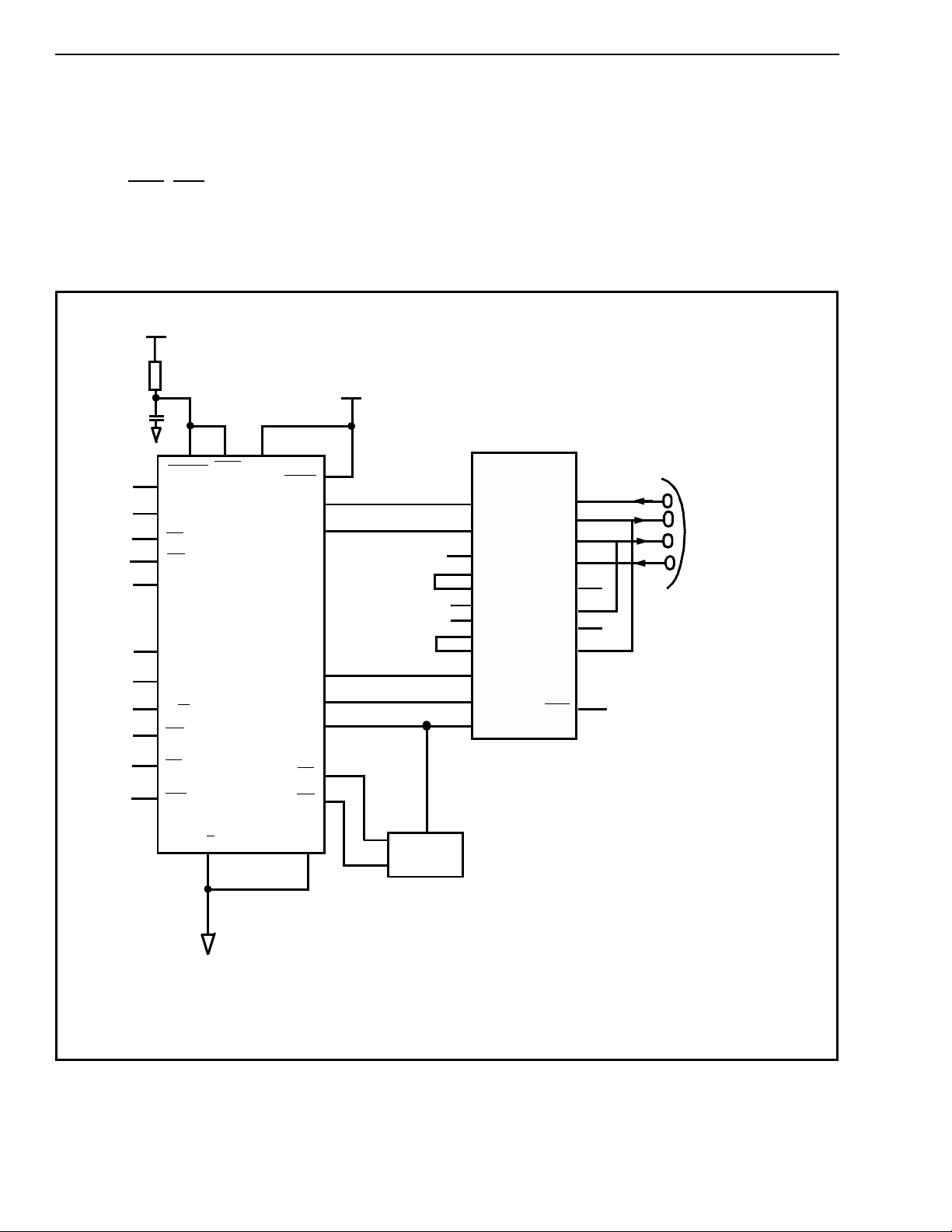
Figure 3a - Application Circuit for 75Ω Operation
Page 5
Preliminary Information MH89793
VDD
10K
0.1µ
33
31
26
32
8-15
18-22
23
24
25
2
7
1
RESET
DSTi
DSTo
F0i
C4i
E8Ko
D0-7
AC0-4
R/W
CS
DS
IRQ
TAIS
MT9079
+5
15
16
13
10
27
28
23
22
21
9
7
8
TZA1
TZA2
TZA3
TZB1
TZB2
MH89793
TxA
TxB
RZA
RZB
RxA
RxB
E2o
RLA
TLA
TLB
RLB
TZD1
TDZ2
TZC1
TZC2
LOS
12
1
3
4
2
11
5
6
25
NETWORK
CONNECTOR
1641
TxMF
TxA
TxB
RxA
RxB
E2i
Foi
C4i
35
43
42
30
29
27
31
26
V
DD
36
S/P
V
SS
MT9042
37
Figure 3b - Applicati on Circu it for 120Ω Operation
4-233
Page 6
MH89793 Preliminary Information
A
A
A
AAAA
AAAA
AAAA
AAAA
A
A
AAA
AAAA
AAAA
AAAA
AAAA
AAAA
AAAA
AAAA
AAAA
AAAA
AAAA
AAAA
AAAA
AAAA
AAAA
0.23 Max
(5.9 Max)
AAA
AAAA
AAAA
AAAA
AAAA
AA
AAAA
AA
AAAA
AA
AAAA
AA
AAAA
AA
0.060 Typ
(1.52)
0.125+0.015±
(3.18+
0.38)
0.063 Ma x
(1.6 Max )
0.050 Typ
(1.27 Typ)
Notes:
1) Not to scale
2) Dimensions in inches).
3) (Dimensions in millimetres).
*Dim en si on s to ce nt re of pi n.
*
0.10 + 0.005
(2.54 +
0.12)
*
0.020 + 0.005
(0.51 + 0.12)
1.42 Max
(36.1 Max)
0.37 Max
(9.5 Max)
0.08 Typ (2 Typ)
1.08 Max
(27. 4 Ma x)
AAA
AAA
AAA
AAA
AAAA
AAAA
AAAA
AAAA
AAAA
AAAA
AAAA
AAAA
AAAA
AAAA
AAAA
AAAA
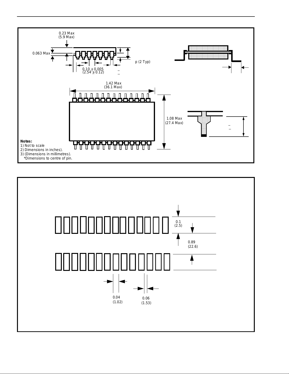
Figure 4 - Mech a nical Data for 28 Pin Sur face M ount Hy brid
0.1
(2.5)
0.89
(22.6)
0.04
(1.02)
0.06
(1.53)
4-234
Figure 5 - Recommended F ootp rint for 28 Pin Surface Mount Hybri d
Page 7
Preliminary Information MH89793
AAAA
AAAA
AAAA
AAAA
A
A
AAA
AAAA
AAAA
AAAA
AAAA
A
A
AAA
0.31 Max
(7.9 Max)
0.08 Typ (2 Typ)
0.100+
0.005
(2.54+
0.12
Notes:
1)Not to scale
2)Dimensions i n inches).
3) (Dimensions in millimetres).
*Dimensions to centre of pin.
*
0.020 + 0.005
0.12)
(0.5 +
0.23 Max (5.9 Max)
*
0.050 Ty p
(1.27 Typ)
1
0.063 Max(1.6 Min)
0.26+
0.015 (6. 6+0.4)
1.42 Max
(36. 1 Ma x)
AAA
AAAA
AAAA
AAAA
AAAA
AAA
AAA
AAA
AAA
AAAA
AAAA
AAAA
AAAA
AAAA
AAAA
AAAA
AAAA
AAAA
AAAA
AAAA
AAAA
AAAA
AAAA
AAAA
AAAA
AA
AA
AA
AA
AA
0.90 Typ
(22.9 Typ)
0.95 Max
(24.2 Max)
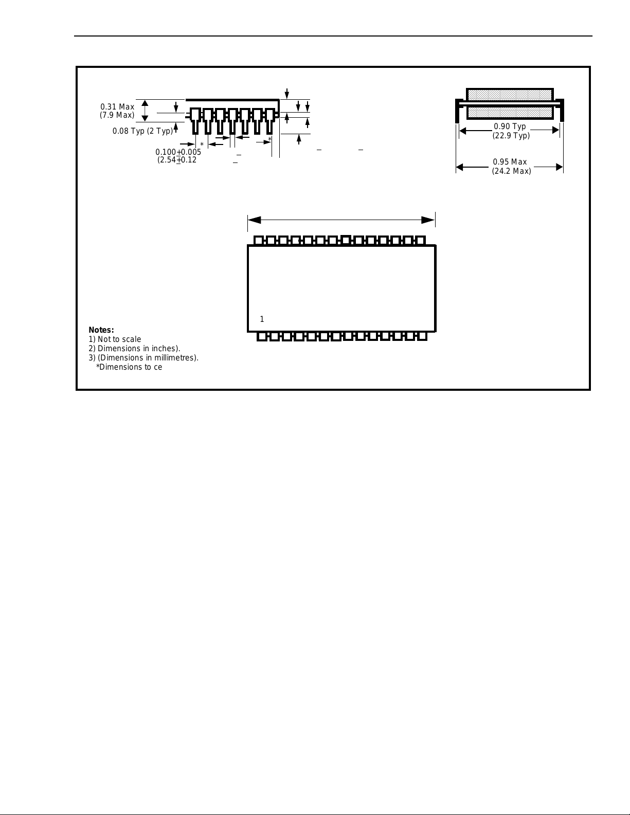
Figure 6 - Mechanical Data for 28 Pin DIL Hybrid
4-235
Page 8

MH89793 Preliminary Information
Notes:
4-236
 Loading...