

Page 1
MH89626C
OPS/DID SLIC
Preliminary Information
Features
• Transformerless 2-4 wire conversion
• Const ant cu rrent wit h const ant voltage fallbac k
for long loops
• Long leng th cap ab ility (R
> 1850Ω)
Loop
• Input i m pedance
•200Ω + 560Ω // 0.1 µF (MH89626C-02)
•200Ω + 680Ω // 0.1 µF (MH89626C-04)
• Ring trip filter with auto ring trip
• Three relay driv ers
• Built-in Tip/Rin g reve rsal cap ab ility on the
hybrid
• Serial control interface
• Extern al or sof twar e progra mm able re ceive
gain, -3.5 or -7 .0dB
Applications
• Off-Premise PBX Line Cards
• DID (Direc t Inward Dial) Line Cards
• Centr al Offic e Line C ards
ISSUE 3 May 1995
Ordering Information
MH89626C-02 38 Pin SIL Package
MH89626C-04 38 Pin SIL Package
0°C to 70°C
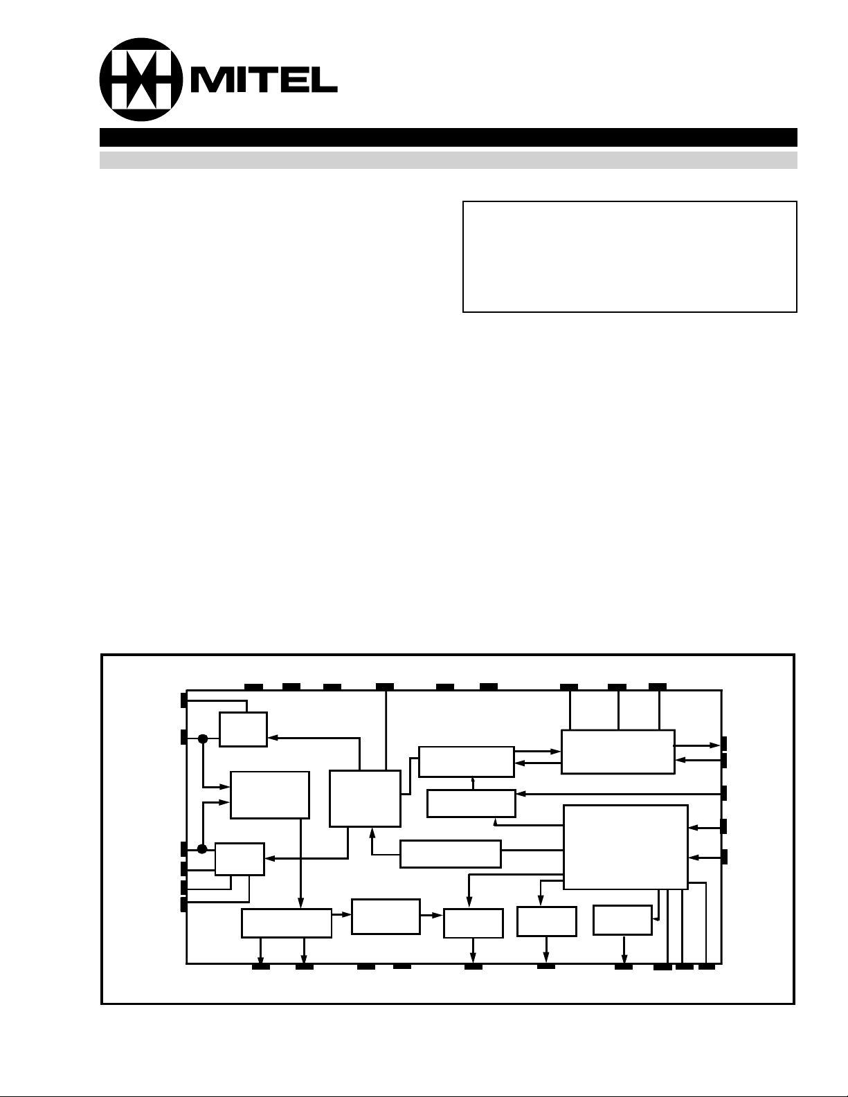
Description
The MH89626C SLIC provides all of the functions
required to interface 2-wire off premise subscriber
loops to a serial TDM, PCM, switching network of a
modern PBX. The MH89626C is manufactured
using thick film hybrid technology which offers high
voltage capability, reliability and high density
resulting in significant printed circuit board area
saving of the line cards. A complete line card can
be implemented with very few external
components.
The SLIC has a simple serial control interface to
control the receive gain setting, relay drivers for
ringing, and Tip/Ring reversal for DID operation.
TF
TIP
RING
RF2
RF
VBat
LGND VDD VEE LCA AGND RGND VREF F1i C2i
Tip
Drive
2W/4W
Current
& Voltage
Sensing
Ring
Drive
Line
Supervision
LED SHK VAC VRLY RD1 RD2 RD3 SD5 SD6 SD7
Constant
Current &
Voltage
Control
Auto Ring
Trip Fil te r
Conversion
Gain
Adjust
Tip/Ring
Reversed
Relay
Drive 1
Relay
Driver 2
Filter/Codec
SD2
SD3
SD0
SD1
MT8967
A-Law
8-Bit
Shift
Register
SD4
Relay
Driver 3
Figure 1 - Functional Block Diagram
Do
Di
GS
CS
SDi
2-285
Page 2
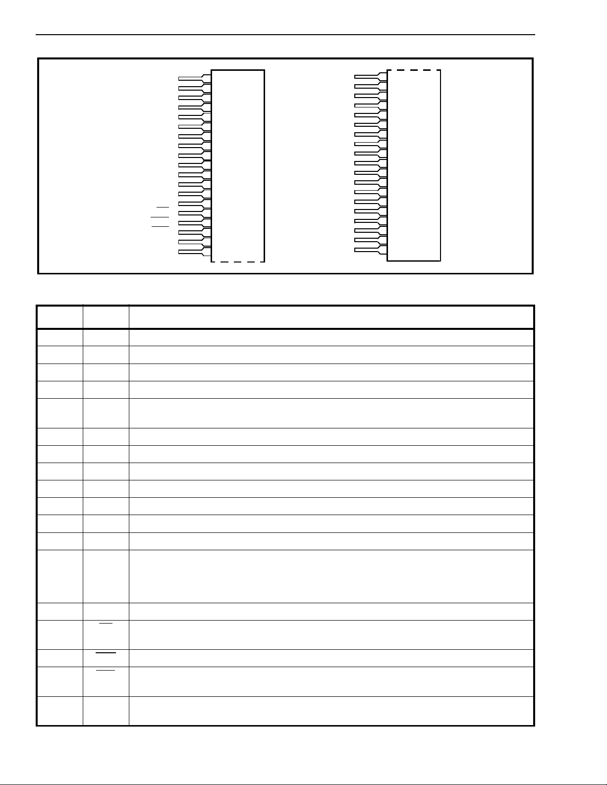
MH89626C Preliminary Information
TIP
RING
RF
TF
LPND
VBat
RF1
RF2
VEE
AGND
VDD
IC
VAC
IC
CS
SHK
LED
LCA
SD1
1
2
3
4
5
6
7
8
9
10
11
12
13
14
15
16
17
18
19
VREF
D1
C2i
Do
F1i
IC
IC
IC
GS
IC
SD7
SD6
SD5
IC
VRLY
RGND
RD2
RD3
RD1
Figure 2 - Pin Connections
Pin Description
Pin # Name Description
1TIPTip Lead: Connects to the TIP lead of the telephone line.
2 RING Ring Lead: Connects to the Ring lead of the telephone line.
20
21
22
23
24
25
26
27
28
29
30
31
32
33
34
35
36
37
38
3RFRing Feed.
4TFTip Feed.
5 LGND Loop Ground: Return path for the battery (V
) supply voltage. Connects to System
Bat
Ground.
6V
Battery Supply Voltage: Normally -48V.
Bat
7RF1Ring Feed 1: Ringi ng input .
8RF2Ring Feed 2: Ring ing output.
9V
Negative Su pp ly Voltage. (-5V).
EE
10 AGND An al og Gr ou nd: Analog and Digital Ground. Connects to system ground.
11 V
Positive Su pp ly Voltage. (+5V).
DD
12 IC Internal Connection.
13 VAC Battery AC Component (input). AC noise present in the V
supply isolated from the DC
Bat
components, can be applied to this pin to reduce longitudinal noise on TIP and RING. To
implement this feature, connect a 0.1µF 100V capacitor from V
to VAC, and 1kΩ resistor
Bat
from VAC to AGND. This pin must be tied to AGND when not used.
14 IC Internal Connection.
15 CS
Chip Select (Input): A TTL compatible digit al inp ut to enable the SDi to control all t he
functions of the driver.
16 SHK Switch Hook Detect (Output): A logic low indicates an off-hook condition .
17 LED
LED Drive (Output).: Drives an LED directly through an internal 2.2kΩ resistor. A logic low
indicates an off-hook condition.
18 LCA L oo p Current Adj ust (in pu t): If this pin is left open, the constant current will be set at
23mA. The loop current can be adjusted by connecting a resistor to V
2-286
EE
.
Page 3
Preliminary Information MH89626C
Pin Description (Continued)
Pin # Name Des crip tio n
19 SDi Serial Data in (input): A TTL compati ble digital input. The 8-bit serial input enables the
driver s. See Table 1 and Figure 3b.
20 V
Voltage Reference (Input) +2.5V for the internal codec.
Ref
21 Di D a ta in (Input) . A TTL compat ibl e digit al input which ac cepts the 8-bit PCM word from the
incoming PCM bu s.
22 C2i Clock input (in pu t). A TTl compatibl e digit al input which ac cepts the 2048 kHz clock.
23 Do Data Out (Output) A three state TTL compatib le digit al out put which drive s the 8-bit PC M
word to the outgoin g PCM bu s.
24 F1i
Synchroni zation input (Inp ut). A TTL compatible, active low digital output input enabling
the PCM input, PCM outp ut and digital control inpu t. It is internally sampled on every
positive edge of the clock, C2i and provides frame and channel synchronization. See fig
3a.
25-27 IC Internal Connection
.
28 GS Gain setting (Input). A logic ‘0’ at this input will set the receiving gain to -7.0dB and a logic
‘1’ will set the receiving gain to -3.5dB. If this pin is left open, the receiving gain can be set
by SDi, bit 2.
29 IC Internal Connection.
30 SD7 S e rial Data (Outpu t). A TTL compatible output comin g from the SDi, bit 7. Bit inverted.
31 SD6 Serial Data (O utput). A TTL compatible output comin g from the SDi, bit 6. Bit inverted.
32 SD5 S e rial Data (Outpu t). A TTL compatible output comin g from the SDi, bit 5. Bit inverted.
33 IC Internal Connection.
34 V
RLY
Relay Positive Supply Voltage. Normally +5V. Connects to the relay coil and the relay
supply voltage.
35 RGND Relay Ground. Return path for relay supply voltage.
36 RD2
Relay Driver 2 (Outpu t). Connects to a user provided external relay coil. A logic ‘0’
from the SDi, bit 1 will activate this driver. This relay driver is typically used for system
in-test.
37 RD3
Relay Driver 3 (Outpu t). Connects to a user provided external relay coil. A logic ‘0’
from the SDi, bit 4 will activate this driver. This relay driver is typically used for system
in-test.
38 RD1
Relay Driver 1 (Outp ut). Connects to a user provided external relay coil. A logic ‘0’ from
the SDi, bit 0 will activate this driver. This relay driver is typically used for ringing.
2-287
Page 4
MH89626C Preliminary Information
Absolute Maximum Ratings*- All voltages are with respect to AGND unless otherwise specified.
Parameter Symbol Min Max Units
1 DC Supply Voltage V
2 DC Battery Voltages ➀ V
3 DC Ring Relay Voltage V
4 DC Reference Volt age V
V
DD
EE
Bat
RLY
REF
-0.3
0.3
0.3 -65 V
-0.3 7 V
-0.3 V
7
-7
DD
5 AC Ring Generator Voltage 150 V
6 DC Digital Input Voltage GS,SDi,Di,
-0.3 V
DD
C2i,F 1 i
7 Storage Temperature TS -40 +125 °C
* Exceeding these values ma y cause perm anen t dama ge. Functi onal operati on und er these cond ition s is not implied.
Recommended Operating Conditions
Parameter Symbol Min TYP* Max Units Comments
1 DC Supply Voltage V
2 DC Battery Volt age ➀ V
3 DC Ring Relay Voltag e V
4 DC Reference Voltage ② V
5 AC Ring Generator Vol tage
Ringing Generator Frequency
6 Operating Temperature T
V
DD
EE
Bat
RLY
REF
OP
4.75
-4.75
5.0
-5.0
5.25
-5.25
V
V
-39.8 -48 -60 V
5.0 7.0 V
2.488 2.500 2.512 V
22 90
25
130
28
V
RMS
Hz
02570°C
V
V
V
RMS
V
➀ LGND is c o nn ec te d t o AGND
② Temperat ure coefficient of V
should be better than 100ppm/C
REF
2-288
Page 5

Preliminary Information MH89626C
DC Electrical Characteristics*
Characteristics Sym Min Typ
†
Max Units Test Comments
1 Supply and Battery Current
➀
Short Loop
Open Loop
2 Power Consumption
3V
Ref
On Hook (V
Powerdown (V
Off-Hook (V
DD
, VEE, V
DD
DC Reference Voltage
Bat
and VEE)
Bat
Mean Current
4SHK
Low Level Output Voltage
High Level Output Voltage
5LED
Low Level Output Voltage
High Level Output Voltage
6RD1
RD2
Sink Current, Relay to VDD
Clamp Diode Current
RD3
7
Low Level Input Voltage
High Level Input Voltage
GS
8 Low Level Input Current
High Level Input Current
I
I
I
I
DD
EE
Bat
Bat
5
12.5
5
11.7
23.5
0
1.5
15
15
28
2
mA
mA
mAmAR
= 0Ω, LCA =Open
Loop
= Open
R
Loop
PC
)
)
100
150
1500
mW
mW
mW
R
R
Loop
Loop
= Open
= 0Ω
2 µA
V
V
②
V
V
I
OL
I
CD
V
V
I
I
OL
OH
OL
OH
IL
IH
IL
IH
-0.3
3.7
2.0
65
100
2.0
0
5
0.5
5.25
3.0 V
V
V
V
IOL = 2mA
= 2mA
I
OH
I
= 1.1mA
OL
= 0.7mA
I
OH
mAmAVOL = 1.0V
0.8 V
V
1
1
µA
µA
VIL = 0V
= 5.0V
V
IH
9SDi
RD
10 Do Low Level Output Voltage
11 SDi
C2i
12 Low Level Input Current
F1i
* DC Electrical Characteristics are over Recommended Operating Conditions with VDD at + 5.0V + 5% unless otherwise stated.
† Typ ical figures are at 25°C with nom inal +
① Supply current and power consumption characteristics are over Recommended Operating Conditions with V
and V
② The LED output consists of a 2.2K Ω resi st or i n se ri es wit h the SHK
Bat
Low Level Input Current
Intermediate Input Current
High Level Input Current
High Level Output Voltage
Tri-State Leakage Current
Low Level Input Current
High Level Input Voltage
Di
High Level Input Current
at -48.0V.
I
IL
I
IM
I
IH
V
OL
V
OH
I
OZ
V
V
I
IL
I
IH
5V supplies and are for design aid only.
4.0
0.1
IL
2.4
IH
HCT output.
10
10
µA
µA
10
0.4 V
mA
0.8 V
10
10
µA
µA
= 5.0V
V
IL
= 0.5V
V
IM
= 5.0V
V
IH
= 1.6mA
I
OL
= 0.1mA
V
I
OH
V
VIL = 0V
= 5.0V
V
IH
at 5.0V, VEE at -5.0V
DD
2-289
Page 6

MH89626C Preliminary Information
Loop Electrical Characteristics*
Characteristics Sym Min Typ
†
Max Units Test Comments
1 Maximum AC Ringing ➀
33 mA 25Hz, V
Bat
Current Rejection
2 Ring Trip Detect Time ② 100 125 ms
3 Hook Switch Detect Time:
Off-Hook to On-Hook
On-Hook to Off-Hook
4 Operating Loop Current I
5 Operating Loop Resistance R
6 Loop Current at Off-Hook ③
IP
IP
18 22 50 mA LCA = Adjustab le
0
0
I
sh
71013mA
20
20
1900
2300
ms
ms
Ω
Ω
V
Bat
V
Bat
= -39.8V
= -48V
Detect Threshold
* Loop Electrical Chara cteri stic s are over Recommend ed Opera ting Condi tions unless ot herwise state d.
† Typical figures are at 25°C with nominal +
① The SLIC can be loaded with an AC impedance as low as 4000Ω without generating a false SHK
8kΩ, the SLIC can drive a REN of 2 without generating a false SHK
② This pa ram e ter is ov e r R e co m me nd ed O p er a tin g C on di tions as w el l a s th e s pecified O p era ting Loop R e si st an ce .
③ Off-Hook Detect ( SHK
) will be detected for loop lengths of 2900Ω or less.
5V supplies and are for design aid only.
output. Since each REN represents
output.
AC Electrical Characteristics*
720
813
51
40
32
65
65
36
24
24
40
30
40
†
Max Units Test Comments
Ω
Ω
dB
dB
dB
dB
dB
dB
dB
dB
1020 Hz
1020 Hz
300 Hz
500-2000 Hz
3400 Hz
300-600 Hz
600-3400 Hz
300 Hz
500-2500 Hz
3400 Hz
Ripple 50mV
1020 Hz
dB
dB
dB
Characteristics Sym Min Typ
1 2- Wire input
Z
in
(200Ω + 560Ω // 0.1µF) −2
Variant
(200Ω + 680Ω // 0.1µF) −4
Variant
2 Ret urn Loss at 2-Wire 14
18
14
3 Long itudinal t o Metalli c Balance 40
46
4 Transhybrid Loss 16
20
16
5 P ower Sup ply Rejecti on Ratio
PSRR
at 2-wire and Do:
V
DD
V
EE
V
Bat
* AC Electrical Characteristics are over Recommended Operating Conditions unless otherwise stated.
† Typical figures are at 25°C with nominal +
5V supplies and are for design aid only.
20
20
20
= -48V
2-290
Page 7

Preliminary Information MH89626C
AC Electrical Characteristics* - Transmit (A/D path)
Characteristics Sym Min Typ
†
Max Units Test Comments
1 Absolute Gain
Default (codec odB)
-0.5 0 0.5 dB Input -6dB
1020 Hz
2 Transmit Gain 0 dB
3 Loss Distortion with frequency
(relative to level at 1020Hz with
codec at 0dB)
4 Gain variation with Input Level
(relative to gain at 1020Hz with
-6dBm input)
5 S ignal Input Overload Level at
2-Wire
0.0
-0.3
-0.3
-0.3
-0.3
-0.3
-0.3
0.39
0.22
-
-
1.0
0.75
0.35
0.55
1.5
dB
dB
dB
dB
dB
dB
dB
0-200 Hz
200-300 Hz
300-400 Hz
400-600 Hz
600-2400 Hz
2400-3000 Hz
3000-3400 Hz
Input 1020 Hz
-0.25
-0.25
-0.5
-1.5
0.25
0.25
0.5
1.5
dB
dB
dB
dB
0 to +3dBm
-40 to 0dBm
-50 to -40dBm
-55 to -50dBm
3.14 dBm THD <
Input 1020Hz
6 S ignal Output Overload Leve l at Do 3.14 dBm0 THD <
Input 1020Hz
7 Signal to Total Distortion Ratio at Do
8 Out-of-Band Discrimination at Do:
Signals in 4.6 -72 kHz band
Signals in 300-3400 Hz band
35
33.8
28.8
19.5
14.5
-50
-40
dB
dB
dB
dB
dB
dBm0
dBm0
Input at 2-Wire
0 to -10dB
-20dBm
-30dBm
-40dBm
-50dBm
Input at 2-wire
-25dBm, 4.6 -72kHz
0dbm, 1020Hz
other than 1020 Hz
Signals in 4.6 -72 kHz band
9 Harm onic Distort ion
-25
dBm0
-41 dB
0dBm, 300 -3400 Hz
(2nd or 3rd Harmonic) at DSTo
10 Idle Channel Noise at Do -70 -64 dBm0p
† Typical figures are at 25°C with nominal +5V supplies and are for design aid only.
* AC Electrical Characteristics are over Recommended Operating Conditions unless otherwise stated.
5%
5%
2-291
Page 8

MH89626C Preliminary Information
AC Electrical* - Receive (D/A) path
Characteristics Sym Min Typ
†
Max Units Test Com me nts
1 Absolu te Gain
(Codec 0dB, GS = 5V)
2 G ain program mable Range
GS = 5V
GS = 0V
3 Lo ss Distortion with Frequency
(relative to level at 1020 Hz with
codec at 0dB and GS = 5V)
4 G ain Variation with Input Level
(relative to gain to 1020Hz with
-10dBm0 input)
5 S ignal Inpu t Overload Level at Di 3.14 dBm TH D <
6 S ign al Output Overload Level at
2-wire
-0.5 0.0 0.5 dB Input -1 0dB m0
1020 Hz
Input - 10dBm0
-3.5
-7.0
-0.3
-0.3
-0.3
-0.3
-0.3
-0.3
-0.3
-0.25
-0.25
-0.5
-1.5
3.14 dBm0 THD <
-0.09
-0.08
-
-
1.0
0.75
0.35
0.55
1.5
0.25
0.25
0.5
1.5
dB
dB
dB
dB
dB
dB
dB
dB
dB
dB
dB
dB
dB
1020 Hz
1020 Hz
Input -10dB m0
0-200 Hz
200-300 Hz
300-400 Hz
400-600 Hz
600-2400 Hz
2400-3000 Hz
3000-3400 Hz
Input 1020 Hz
0 to +3dBm
-40 to 0dBm
-50 to -40dBm
-55 to -55dBm
Input 1020Hz
Input 1020Hz
5%
5%
7 S ign al Out put to Total
Distortion Ratio at 2-Wire 35
32.9
24.9
19.9
8 O ut-of -B and Discriminat ion at
2-Wire:
Signals in 4.6 -72 kHz band
Signals in 300-3400 Hz band
other than 1020 Hz
Signals in 4.6 -72 kHz band
9 Harm onic Distortion
(2nd or 3rd Harmonic) at 2-Wire
10 Idle Channel Noise at
2-Wire -73
-73
* AC Electrical Characteristics are over Recommended Operating Conditions unless otherwise stated.
† Typical figures are at 25°C with nominal +
5V supplies and are for design aid only.
-50
-40
-25
-41 dB
-67
-67
dB
dB
dB
dB
dBm
dBm
dBm
dBmp
dBmp
Input at 2-Wire
0 to -20dB
-30dBm
-40dBm
-50dBm
Input at Di
-25dBm0, 4.6 -72kHz
0dBm0, 1020 Hz
0dBm0, 300-3400 Hz
Gain Setting
-3.5dB
-7dB
2-292
Page 9

Preliminary Information MH89626C
Loop Electrical Characteristics
Characteristics Sym Min Typ* Max Units Test Comments
f
1 Clock Frequency C2i
2 Clock Rise Time C2i t
D
3 Cl ock Fall Ti me C2i t
I
4 Clock Duty Cycle C2i 40 50 60 %
G
5 Chip Ena ble Rise Time F1i
I
6 Chip Ena ble Fal l Time F1i
T
A
7 Propagation Delay Clock
L
to Output Enable
Do t
t
t
PZL
t
PZH
2.046 2 .048 2.05 MHz
C
CR
CF
ER
EF
50 ns
50 ns
100 ns
100 ns
122
122
ns
ns
RL = 10kΩ to V
CL = 100pF
CC
8 Input Setup Time Di t
9 Input Hold Time Di t
* Typical figures are at 25°C with nominal +5V supplies. For design aid only: not guaranteed and not subject to production testing.
ISH
t
ISL
IH
25
0
60 ns
ns
ns
Bit Name Description
0
1
2
SD0 When Logi c ‘0’ activate s relay driver 1 to apply ringing to the line
SD1 When logi c ‘0’ activat es relay driver 2. Normally used for in-te st
SD2 When logi c ‘0’ it will set the receive gain to -7. 0dB
When logic ‘1’ it will set the receive gain to -3.5 dB
3
4
5
6
7
SD3 When logic ‘0’ reverses the TIP and RING.
SD4 When logi c ‘0’ activat es relay driver 3. Normally used for out-test
SD5 The output of the serial data stream SDi , bit 5. Bit inverted
SD6 The output of the serial data stream SDi , bit 6. Bit inverted
SD7 The output of the serial data stream SDi , bit 7. Bit inverted
Table 1 - Control of SLIC Functions through SD
2-293
Page 10

MH89626C Preliminary Info rm atio n
Functional Desc ription
The MITEL MH89626C OPS SLIC (Off-Premise
Subscriber Line Interface Circuit) provides a
complete interface between an off-premise
telephone line and a digital switching system. All
BORSCHT functions are provided requiring only a
few external components. The input impedance
conforms with Chinese standard requirements.
Overvoltage Pr otection
The MH89626C is protected f rom short term (20ms)
transi ents (+
Ground, and RING and Ground. However, if the
MH89626C is used in conjunction with MH80626C,
protection sip, it will meet all CCITT K.20
requirements. The applications circuit is shown in
Figure 2.
The MH80626C has two battery feed resistors (50
ohms) and one ringing feed resistor (560 ohms), that
are required to be used with the MH89626C as a
complete line interface. All resistors on the hybrid
are specially designed to withstand high power. The
two battery fe ed resistors are accurate ly trimmed to
achieve good longitudinal balance. Two fuses and
current limited resistors (5 ohms) are provided on the
hybrid for lightning and high voltage surge
protection.
250V) between TIP and RING, TIp and
Battery Feed
The MH89626C powers the telephone set with
constant DC loop current for short lines and
automatically reverts to constant voltage for long
lines. If th e LCA pin is left open, the constant cur ren t
is set at 23 mA. The Constant current can also be
set by adding a resistor connected fro the LCA pin to
V
. The resistance (R) can be calculated as:
EE
147.2 - I
R=
(0.0001176 X I
Loop
) - 0.002586
Loop
TIP/RING Reversa l
For a Direct Inward Dialling (DID) operation, the
MH89626C provides a TIP and RING reversal
function on the hybrid. This built-in line polarity
reversal capability will eliminate the use of an
external bulky mechanical relay and provides fast
and reliable Tip and Ring reversed function. The
serial control stream, SDi, bit 3 at logic low will
reverse the polarity of the Tip and Ring. Refer to
Table 1 for control of the SLIC functions.
Ringing
The ringing insertion circuitry has the capability to
provide ringing v oltage to a telephone set by simply
adding an external relay, ring generator. The serial
control stream, SDi, bit 0 at logic low will activate the
Refer to Table 1 for the control of SLIC functions.
Supervision
The loop detection circuit determines whether a low
enough impedance is across Tip and Ring to be
recognized as an off-hook condition. When an
off-hook condition occurs, the SHK
outputs toggle to a low level. These outputs also
toggle with incoming dial pulses.
During applied ringing, the loop detection circuit
engages a ringing filter. This filter prevents a false
off-hook detection due to the current associated with
the AC ringing voltage as well as current transients
that occur when the ringing voltage is switched in
and out. The Ring trip detection circuitry deactivat es
the ring driv er after an off-hook condition is detected.
and the LED
Transmit and Receive Gain
The Transmit Gain (Tip-Ring to Do) is fixed at 0dB.
The Receive Gain (Di to Tip-Ring) is programmable
in -3.5 or -7.0dB, either using software (SDi, bit 2) or
external hardware (GS pin).
Where I
mA, and R is the resistance from pin LCA to pin V
in ohms.
R(kΩ) 348K 200K 80K 50K 30K
I
Loop
(mA)
2-294
is the desired constant loop current in
Loop
25.0 27.1 34.0 40.2 49.7
EE
Page 11

Preliminary Information MH89626C
MH80626C
Test
Test
Tip
Ring
Components
D1,D2,D3,D4 IN4004
Q1 = FET BUZ 22 or equivalent
R1 = 10k Ω +5%
R2 = 1k Ω + 5%
C1 = 0.01µF + 10% 100V
PTC = 55Ω, 50mA
Out
K3A
K3B
In
K2A
20
K2B
1
1
/4W
1
TIN
RIN
-48V
/4W
90
TOUT
ROUT
VRMS
TF
RF2
RF1
25Hz
RF
K1A
5
D1
6
T
14
12
7
R
8
R1
R2
K1B
-48V
D2
Q1
Heat sink 9
18
16
+5V
K1 RELAY
K2 RELAY
PTC
K3 RELAY
C1
D3
D4
to other
circuit
o
C/W
30
31
32
38
36
371
34
1
TIP
4
TF
3
RF
2
RING
8
RF2
7
RF1
SD7
SD6
SD5
RD1
RD2
RD3
VRLY
MH896 26C
F1i
VRef
C2i
Do
GS
SDi
CS
LED
SHK
VAC
LGND
VBat
LCA
24
20
22
23
Di
21
28
19
15
17
16
13
5
6
-48V
18
VDD VE E AGND RGND
31
9
30 18
290V
TISP
+5V -5V
C2i
t
F1i
PHZ
Do
Di
Figure 3 - Application Circuit
t
t
ES
ISH
t
ES
t
PZH
t
PZL
t
ISL
t
PLH
t
PHL
t
IH
Figure 4a - Control Timing Diagra m
2-295
Page 12

MH89626C Preliminary Information
C2i
CS
SD1
Side View
b7
0.010 +
(0.25 +
0.002
0.05)
0.12 Max
(3.0 Max)
0.27 Max
(6.9 Max)
b6
b5
Figure 4b -Control Timing Diag ram
0.02
0.58+
0.5)
(14.7+
1 2 3 4 37 38
b2
b1
3.80 + 0.0 15
1.4)
(9.652 +
b0
Notes:
1) Not to scale
2)Dimensions in inch es).
3) (Dimensions in millimetres).
*Dimensio ns to centre of pin &
tolerance non ac cumulati ve.
2-296
0.01
0.5)
*
***
0.25 +
0.02
(6.4 +
0.05)
0.05 +
(1.3 +
Figure 5 - Mechanical Data
0.020 +
(0.51 +
0.005
0.13)
0.100 +
(2.54 +
0.010
0.26)
0.18 +
(4.6 +
0.02
0.5)
 Loading...