

Page 1
MH89625C
OPS/DID PCM SLIC
Preliminary Information
Features
• Input impe dance v aria nts:
- 600Ω
- 200Ω + 680Ω // 0.1µF
- 200Ω + 560Ω // 0.1µF
• Operates wi th a wide rang e of bat tery vol tag es
• Constant current battery feed with constant
voltage fall back for long l oop dri ve ca pabiliti es
• Overvoltag e and s hort circuit pro tect ion
• Off-hook detection and LED indicator drive
• Dial pulse detection
• Ring trip filter with auto ring trip
• Ring relay dr iver pl us thre e mor e uncom mitte d
relay drivers
• Transformerless 2W to 4W conversion
• A/D and D/A c onvers ion
• Conforms to A-Law PCM
• Analog and digi tal loop ba ck
• Conforms to CC ITT k .20 overv olta ge su rge
requirements with external primary protection
circuitry
Applications
• Off premise digital PBX line cards
• DID (Direct Inward Dial) lin e cards
• PABX, Key Systems, Central Office Equipment
ISSUE 4 May 1995
Ordering Information
MH89625 C 600Ω
MH89625C- 5 200Ω + 680Ω // 0.1µF
MH89625C- 6 200Ω + 560Ω // 0.1µF
40 Pin DIL Package
Description
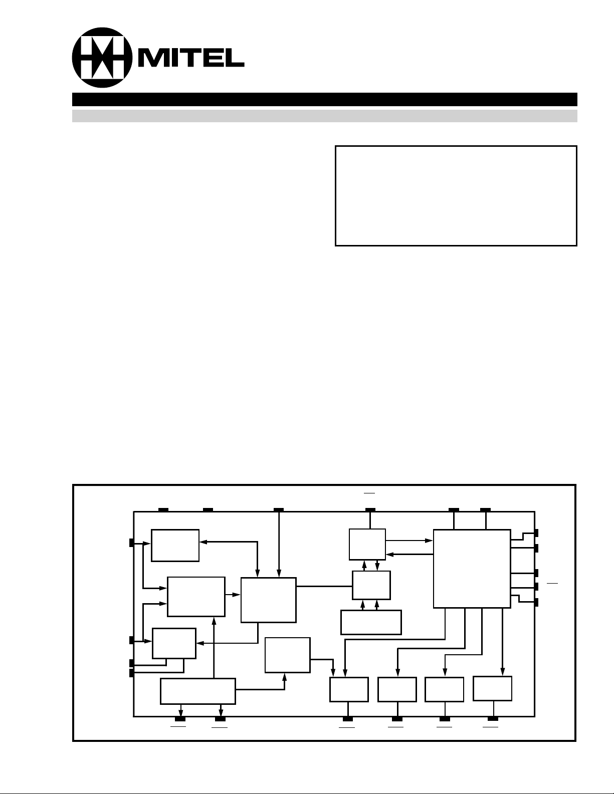
The Mitel MH89625C SLIC (Subscriber Line
Interface Circuit) provides a complete interface
between an off-premise telephone line and a digital
switching system. All BORSCHT functions of Battery
Feed, Overvoltage Protection, Ringing Feed, Line
Supervision, Codec, 2-4 Wire Hybrid and Test are
provided requiring only a few external components.
The input impedance conforms with Chinese
standard requirements. The device is fabricated
using thick film hybrid technology which incorporates
various technologies for high voltage capability,
optimum circuit design and very high reliability.
TIP
RING
RF2
RF1
VBat LGND LCA GS
Tip
Drive
Current
& Voltage
Sensin g
Ring
Drive
Supervision
LED
Constant
Current &
Voltage
Control
Ring
Trip
Filter
Line
Gain
Adjust
2w/4w
hybrid
Impedance
Matching
Relay
Driver 1
RD1SHK
Figure 1 - Functional Block Diagram
Relay
Driver 2
VX
VR
Relay
Driver 3
RD3RD2
VREF CA
VREF
CODEC
CA
DSTo
DSTi
CSTi
SD2SD1SD0
Relay
Driver 4
RD4
F1i
CS
SD3
DSTi
DSTo
CSTi
F1i
C2i
2-269
Page 2
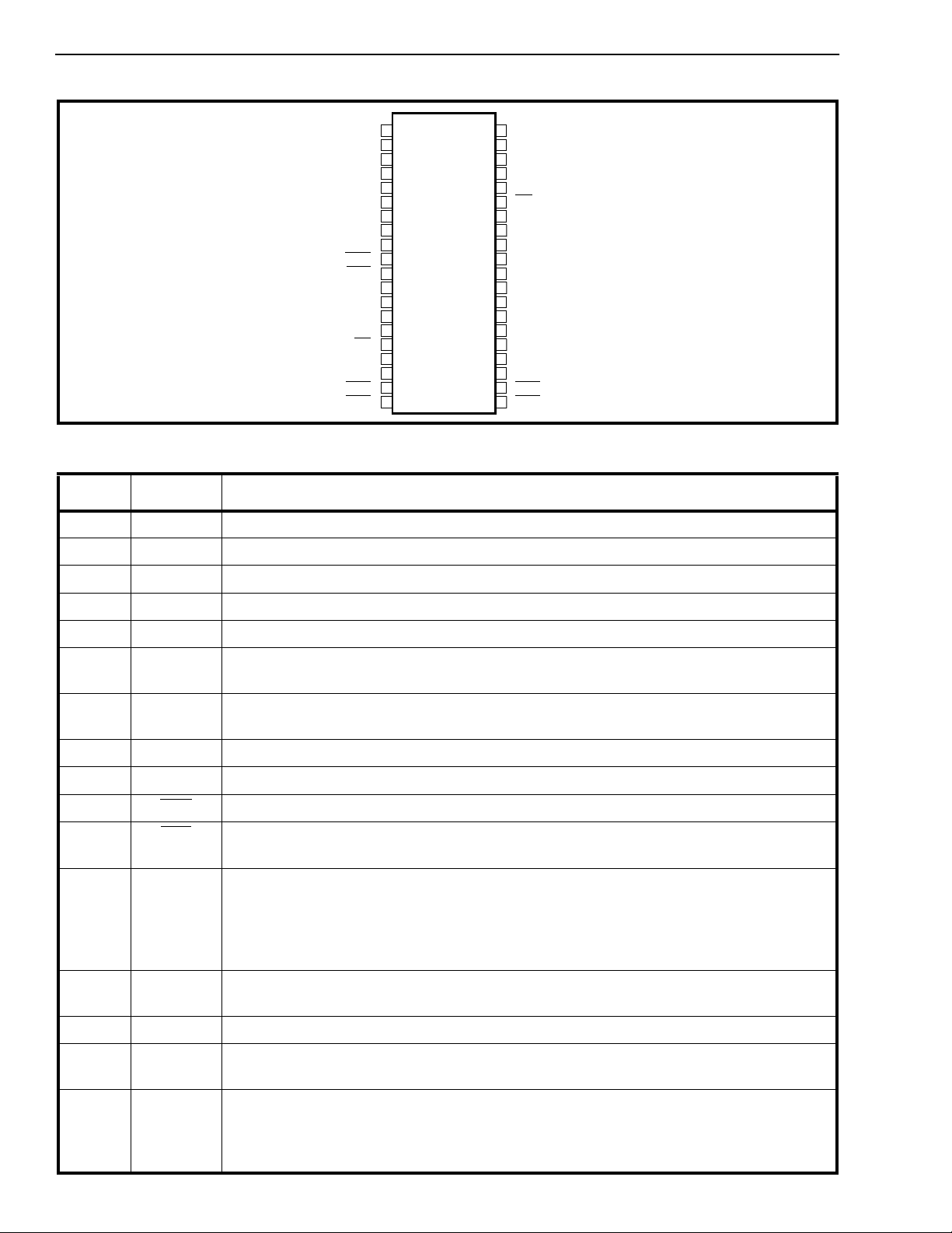
MH89625C Preliminary Information
TIP
RING
IC
IC
IC
RF1
RF2
IC
VEE
SHK
LED
CSTi
DSTi
C2i
DSTo
F1i
CA
RGND
RD2
RD1
1
2
3
4
5
6
7
8
9
10
11
12
13
14
15
16
17
18
19
20
40
39
38
37
36
35
34
33
32
31
30
29
28
27
26
25
24
23
22
21
IC
IC
IC
VBAT
LGND
GS
VAC
IC
LCA
VDD
AGND
IC
IC
IC
IC
IC
VREF
VRLY
RD4
RD3
Figure 2 - Pin Connections
Pin Description
Pin # Name Description
1TIPTip Lead. Connects to the “Tip” lead of the telephone line.
2 RING Ring Lead. Connects to the “Ring” lead of the telephone lin e.
3ICInternal Connection : This pin is internally connected.
4ICInternal Connection : This pin is internally connected.
5ICInternal Connection : This pin is internally connected.
6RF1Ring Feed 1: For OPS operation, connects to the external battery backed ringing
generator, see Figure 2.
7RF2Ring Feed 2: For OPS operation, connects to RING through a normal ly closed relay
contact (K1), see Figure 2.
8ICInternal Connection. This pin is internally connected.
9V
EE
10 SHK
11 LED
Negative Supply Voltage: (-5V)
Switch Hook Detect (Output): A logic low indicates an off-hook condition.
LED Drive (Output ): Drives an LED directly through an internal 2.2kΩ resistor. A logic
low indicates an off-hook condition.
12 CSTi Control ST-BUS in (Input): A TTL compatible digi tal input used to control the function
of the filter/codec. Three mode s of operati on may be affected by applying to this input
logic high, logic low or an 8-bit serial word, depending on the logic states of CA and F1i.
Functions controlled are: power down, filt er gain adjust , loopbac k, chip testing, and the
SD outputs which control the relay drivers, ring trip circuitry and impedance selection.
13 DSTi Data ST-BUS in (Input): A TTL compatible digital input which accepts the 8-bit PCM
word from the incoming PCM bus.
14 C2i Clock Input (Input): A TTL compatible dig ital input which accepts the 2048 kHz clock.
15 DSTo Data ST-BUS Out (Output). A three stage TTL compa tible digit al out put which drive s
the 8-bit PCM word to the outgoing PCM b us.
16 F1i Synchronization Input (Input): A TTL compatible active low digi tal input enabling (in
conjunction with CA) the PCM input, PCM out put and digit al control input. It is internally
sampled on every positive edge of the clock, C2i, and provides frame and channel
synchronizati on.
2-270
Page 3
Preliminary Information MH89625C
Pin Description (Contin ue d)
Pin # Name Description
17 CA Control Address (Input): A three-level digital input which enables PCM input and
output, and determi nes into whi ch control registe r (A or B) the serial dat a, present ed to
CSTi, is stored.
18 RGND Relay Gro und: Return path for relay supply voltage.
19 RD2
Relay Driver 2: Connects to a user provided external relay coil. A logic high at the SD1
output of the internal MT8967 codec activate s this driver. An internal clamp diode from
is provided. This relay is typically used for DID reversals.
20 RD1
VRLY to RD2
Relay Driver 1. Connects to a user provided external relay coil. A logic high at the SD0
output of the internal MT8967 codec activate s this driver. An internal clamp diode from
is provided. This relay is typically used for ringing.
21 RD3
VRLY to RD1
Relay Driver 3. Connects to a user provided external relay coil. A logic high at the SD2
output of the internal MT89 67 codec activate s this drive r. An internal clamp diode from
is provided. This relay is typically used for in-test.
22 RD4
VRLY to RD3
Relay Driver 4: Connects to a user provided external relay coil. A logic high at the SD3
output of the internal MT8967 codec activate s this driver. An internal clamp diode from
is provided. This relay is typically used for out-test.
23 V
RLY
VRLY to RD4
Relay Positive Supply Voltage: Normally +5V. Connects to the relay coil and the relay
supply voltage.
24 V
Ref
Voltage Reference (Input): +2.50V for the internal codec.
25 IC Internal Connec tion: This pin is internally connected.
26 IC Internal Connec tion: This pin is internally connected
27 IC Internal Connec tion: This pin is internally connected
28 IC Internal Connec tion: This pin is internally connected
29 IC Internal Connec tion: This pin is internally connected
30 AGND Analog Gro und . Analo g and Digital Ground. Connects to System Ground.
31 V
DD
Positive Supply V o ltage (+5V)
32 LCA Loop Current Adjust (Input). The maximum constant loop current is a function of the
resistance connected from this pin to V
. Normally left open
EE
33 IC Internal Connec tion. This pin is internally connected.
34 VAC Battery AC Component (Input). AC noise present in the V
supply, isolated from the
BAT
DC component, can be applied to this pin to reduce longitudinal noise on TIP and RING.
To implement this feature, connect a 0.1µF 100V capacitor from V
to VAC, and a 1kΩ
BA T
resistor from VAC to AGND. This pin must be tied to AGND when not used.
35 GS Gain Setting (In put). A logic low at this input adds an additio nal -0.5d B gain in the
receive direction (DSTi to Tip-Ring). This gain is in addition to the gain set by the Codec.
A logic high adds 0dB gain.
36 LGND Loop Ground. Return path for the batt er y (V
) supply voltage. Connects to System
BAT
Ground.
37 V
Bat
Battery Supply Voltage. Normally -48V.
38 IC Internal Connec tion: This pin is internally connected
39 IC Internal Connec tion: This pin is internally connected
40 IC Internal Connec tion: This pin is internally connected
2-271
Page 4

MH89625C Preliminary Info rm atio n
Functional Desc ription
The Mitel MH89625C OPS SLIC (Off-Premise
Subscriber Line Interface Circuit) provides a
complete interface between an off-premise
telephone line and an digital switching system. All
BORSCHT functions are provided requiring only a
few external components. The input impedance
conforms with Chinese standard requirements.
All functions of the SLIC are controlled by the system
Drive (SD) outputs of the internal Mitel A-Law Codec
MT8967. The SD outputs are controlled by the serial
data input stream at CSTi.
The BORSCHT Functions
The MH89625C performs all of the BORSCHT
functions of Battery Feed, Overvoltage Protection,
Ringing, Supervision, Codec, Hybrid and Test.
Battery Feed
Ringing
The ringing insertion circuit has the capability to
provide ringing voltage to a telephone set by simply
adding an external relay, ring generator and a
transient protector. The internal relay driver switches
ringing voltage onto the line via the external ring
relay. A clamp diode is included which suppresses
voltage transients during relay switching caused by
the relay coil. The serial data input at CSTi controls
the internal Codec’s SDo output which activates the
ring driver. Refer to Table 1 for control of SLIC
functions.
Supervision
The loop detection circuit determines whether a low
enough resistance is across Tip and Ring to be
recognized as an off-hook condition. When an
off-hook condition occurs, the SHK
LED
output can drive an LED directly) outputs toggle
to a low level. These outputs also toggle with
incoming dial pulses.
and LED (the
The MH89625C powers the telephone set with
constant DC loop current for short lines and
automatically reverts to constant voltage for long
lines. The constant loop current is a function of the
resistance connected from the LCA pin to V
Where I
147.2 -I
R =
(0.0001176 X I
is the desired constant loop current in mA,
Loop
Loop
) -0.002586
Loop
and R is the resistance from pin LCA to pin V
EE.
EE
in
ohms.
R (kΩ)
I
Loop
(mA)
open 348k 200k
80k 50k 30k
22.0 25.0 27.1 34.0 40.2 49.7
Overvoltage Pr otection
The MH89625C is protected from short term (20ms)
transi ents (+
ground, and RING and ground. However, additional
protection circuitry may be needed depending on the
requirements which must be met. Normally simple
external shunt protection as shown in Figure 4 is all
that is required.
250V) between TIP and RING, TIP and
During applied ringing (ring relay driver activated),
the loop detection circuit engages a ringing filter.
This filter prevents false off-hook detection due to
the current associated with the AC ringing voltage as
well as current transients that occur when the ringing
voltage is switched in and out. The ring trip detection
circuitry deactivates the ring relay driver after an
off-hook condition is detected.
Codec
The Codec function of the SLIC is implemented
using the Mitel MT8967 A-Law Codec. This device
provides the conversion interface between the
voiceband analog signals of a telephone subscriber
loop and the digital signals required in a digital PCM
(pulse code modulation) system. Eight-bit PCM
encoded digital data enters and leaves the chip
serially on DSTi and DSTo pins, respectively.
For detailed information on the CODEC portion of
the MH89625C, refer to the MT8967 integrated PCM
Filer/Codec data sheet (Microelectronics Digital
Communications Handbook, Mitel Semiconductor
Issue 9).
2-272
Page 5
Preliminary Information MH89625C
Absolute Maximum Ratings* - All voltages are with respect to AGND unless otherwise specified.
Parameter Symbol Min Max Units
1 DC Supply Voltage V
2 DC Battery Voltage ① V
3 DC Ring Relay Voltage V
4 DC Reference Voltage V
V
DD
EE
BAT
RLY
REF
-0.3
0.3
0.3 -65 V
-0.3 7 V
-0.3 V
7
-7
DD
5 AC Ring Generator Voltage 150 V
6 DC Digital Input Voltage
GS, CSTi
-0.3 V
DD
DSTi, C2i
F1i
7 DC Digital (3-level) Input voltage CA V
EE
V
DD
8 Storage Temperature TS -40 +125 °C
* Exceeding these values ma y cause perm anen t dama ge. Functi onal operati on und er these cond ition s is not implied.
① LGND is c o nn ec te d t o AGND
Recommended Operating Conditions
Paramete rs Sym Min Typ
‡
Max Units Test Conditions
.
V
V
RMS
V
V
1 DC Supply Voltages V
2 DC Battery Voltage ① V
3 DC Ring Relay Voltage V
4 DC Reference Voltage ② V
5 AC Ringing Generator
Voltage
V
DD
EE
BAT
RLY
REF
4.75
-4.75
5.0
-5.0
5.25
-5.25
-39.8 -48 -60 V
5.0 7 V
2.488 2.500 2.512 V
22 90
25
130
28
V
Hz
V
V
RMS
Ringing Generator
Frequency
6 Operating Temperature T
① LGND is c o nn ec te d t o AGND.
② Temperature coefficient of V
‡ Typical figures are at 25°C and are for desi gn aid only: not gua rantee d and not subje ct to producti on testing.
should be better than 100ppm/C.
REF
OP
02570°C
2-273
Page 6

MH89625C Preliminary Information
DC Electrical Characteristics†
Characteristics Sym Min Typ
‡
Max Units Test Conditions
1 Supply and Battery Current ①
Short Loop
Open Loop
2 Power Consumption ①
3REF
On-Hook (V
Powerdown (V
Off-Hook (V
DD
DD,VEE,VBAT
DC Reference Voltage
BAT
and VEE)
I
I
I
BAT
I
BAT
DD
EE
8.7
8.4
23.5
1.5
15
15
28
mA
mA
mA
2
mA
PC
)
)
100
150
1500
mW
mW
mW
2 µA
LCA = Open
= 0Ω
R
Loop
= Open
R
Loop
LCA = Open
=Open
R
Loop
R
= 0Ω
Loop
Mean Current
4SHK
5LED
6RD1
RD2
Low Level Output Voltage
High level Output Voltage
Low Level O utput Voltage ②
High Level Output Voltage
Sink Current, Relay to V
DD
Clamp Diode Current
V
V
V
V
I
OL
I
CD
OL
OH
OL
OH
-0.3
3.7
2.0
65
100
0.5
5.25
3.0 V
V
IOL = 2mA
V
V
= 2mA
I
OH
I
= 1.1mA
OL
= 0.7mA
I
OH
mAmAVOL = 1.0V
RD3
RD4
7GS
8 Low Level Input Current
9
CA
10 Low Level Input Current
RD
11 DSTo Low Level Output Voltage
12 CSTi
DSTi
C2i
13 Low Level Input Current
F1i
† DC Electrical Characteristics are over Recommended Operating Conditions with VDD at +5.0V ± 5% and VEE at -5.0V ±5% unless otherwise
stated.
‡ Typical figures are at 25°C with nominal ± 5V supplies and are for design aid only.
① Supply cu rr e nt a nd po w er c on su m pti on ch ar a c teristics are o ve r R ec om m en d ed Op era ting Conditio ns w ith V
and V
② The LED output consists of a 2.2kΩ resi st or in se r ie s wi t h the SHK
NOTE 1: Powe r d ow n m od e i s ac ti va te d t hro ugh the CSTi in pu t da ta st r ea m. Re fer to Table 2.
BAT
Low Level Input Voltage
High Level Input Voltage
High Level Input Current
Low Level Input Voltage
Intermediate Input Voltage
High Level Input Voltage
High Level Input Current
High Level Input Current
High Level Input Voltage
Tri-State Leakage Current
Low Level Input Voltage
High Level Input Voltage
High Level Input Current
at -48.0V
V
IL
V
I
IL
I
IH
V
V
V
I
IL
I
IM
I
IH
V
OL
V
OH
I
OZ
V
V
I
IL
I
IH
2.0
IH
IL
0.0
IM
2.4
IH
4.0
0.1
IL
2.4
IH
HCT output.
0.8 V
1
1
-3.5
0.8
10
10
10
0.4 V
mA
0.8 V
10
10
V
µΑµΑVIL = 0V
= 5.0V
V
IH
V
V
V
µAµAV
V
= 5.0V
IL
= 0.5V
V
IM
= 5.0V
V
IH
= 1.6mA
I
OL
= 0.1mA
I
OH
V
µAµAVIL = 0V
= 5.0V
V
IH
at 5.0V, VEE at -5.0V
DD
2-274
Page 7

Preliminary Information MH89625C
Loop Electrical Characteristics† -
Characteristics Sym Min Typ‡Max Units Test Con ditio ns
1 Maximum AC Ringing ①
33 mA 25Hz, V
BAT
Current Rejection
2 Ring Trip Detect Time ② 100 ms
3 Hook Switch Detect Time:
Off-Hook to On-Hook
On-Hook to Off-Hook
4 Operating Loop Currents
Maximum Operating Loop Current
5 Operating Loop Resistance R
6 Loop Current at Off-Hook ③
I
IP
18 22
50261850
IP
0
0 2300
I
SH
71013mA
20
20
ms
ms
mA LCA= Open
LCA= 30k to V
Ω
V
= -40V
BAT
Ω
=-48V
V
BAT
Detect Threshold
† Loop Electrical Characteristics are over Recommended Operating Conditions unless otherwise stated.
‡ Typical figures are at 25°C with nominal ±5V supplies and are for design aid only.
① The SLIC can be loaded with an AC impedance as low as 4000Ω without g en era ti ng a fal s e SHK
repres en ts 8k Ω, the SLIC can driv e a R EN of 2 w ith ou t g en erating a fa ls e SHK
② This parameter is over Recommended Operating Conditions as well as the specified Operating Loop Resistance.
③ Off-Hook Detec t ( SHK
) will be detecte d f or loop leng th s o f 29 00 Ω or less.
output.
output. Since each REN
AC Electrical Characteristics†
Characteristics Sym Min Typ
‡
Max Units Test Conditions
= -48V
EE
1 2-wire Input Impedance ①
600R
(Magnitu de) 560 Network
(Magnitude) 680 Network
2 Return Loss at 2-Wire ② 14
3 Longitudinal to Metallic
Balance
4 Transhybrid Loss ➁ 16
5 Power Supply Rejection Ratio
at 2-Wire and DSTo:
V
DD
V
EE
V
BAT
† AC Electrical Characteristics are over Recommended Operating Conditions unless otherwise stated.
‡ Typical figures are at 25°C and are for design aid only.
① Three impedance sele ctio ns of Z
② Values ap pl y for all three im pe dances selec ti ons; in all th ree c as es Z
Note 1: All of the ab ov e tes t co nd itions use 200Hz to 34 00 H z un le s s o th er wise stated .
Note 2: The transmi t c od ec g ai n is s et to 0d B , t he r e ce ive codec gain is s e t to 0dB, and th e r eceive gain adj us tm e nt is s et to 0dB
Note 3: With the transm i t an d r e ce iv e g ai ns se t to 0dB ; 0d B m O at the DSTi input will ap pe ar a s 0 dBm at the Tip- Ring output; 0dBm at
Note 4 All dBm is re ferenced to 60 0Ω.
=5V), unless otherwise specified.
(GS
the Tip-Ring input will appear as 0dBmO at the DSTo output.
= 600 Ω, Zin=200Ω + 560 // 0.1µF, and Zin=200Ω + 680 // 0.1 µF are available.
in
Z
in
PSRR
18
14
40
46
20
16
20
20
20
600
720
813
23
24
35
54
51
52
41
52
40
30
40
= Refer e nc e Im pe da nc e .
in
Ω
Ω
Ω
dB
dB
dB
dB
dB
dB
dB
dB
dB
dB
dB
1020 Hz
300 Hz
500-2000 Hz
3400 Hz
300-600 Hz
600-3400 Hz
300 Hz
500-2500 Hz
3400 Hz
Ripple 50mV
1020 Hz
2-275
Page 8

MH89625C Preliminary Information
AC Electrical Characteristics† - Transmit (A/D) Path
Characteristics Sym Min Typ‡Max Units Test Conditions
1 Absolute Gain
Default (Codec 0dB )
-0.5 0 0.5 dB Inpu t -6dBm
1020 Hz
2 Gain Programmable Range ① 0 7 dB 1020 Hz
3 Loss Distortion with Frequency
(relative to level at 1020Hz
with codec at 0dB)
4 Gain Variation with Input Level
(relative to gain at 1020Hz with
-6dBm input)
5 Signal input Overload Level at
2-Wire
6 Signal Output Overload Level at
DSTo
7 Signal to Total Distortion Ratio at
DSTo 35
0.0
-0.3
-0.3
-0.3
-0.3
-0.3
-0.3
-
-
1.0
0.75
0.35
0.55
1.5
dB
dB
dB
dB
dB
dB
dB
0-200 Hz
200-300 Hz
300-400 Hz
400-600 Hz
600-2400 Hz
2400-3000 Hz
3000-3400 Hz
Input 1020 Hz
-0.25
-0.25
-0.5
-1.5
0.25
0.25
0.5
1.5
dB
dB
dB
dB
0 to + 3dBm
-40 to 0dBm
-50 to -40dBm
-55 to-50dBm
3.14 dBm THD <
Input 1020 Hz
3.14 dBm0 T H D <
Input 1020 Hz
Input at 2-Wire
33.8
28.8
19.5
14.5
dB
dB
dB
dB
dB
0 to -10dBm
-20dBm
-30dBm
-40dBm
-50dBm
5%
5%
8 Out-of-Band Discrim inat ion at
Input at 2-Wire
DSTo:
Signals in 4.6 -72 kHz band
Signals in 300 -3400 Hz band
-50
-40
dBm0
dBm0
-25dBm, 4.6 -72kHz
0dB, 1020 Hz
other than 1020Hz
Signals in 4.6 -72 kHz band
9 Harmonic Distortion
-25
dBm0
-41 dB
0dBm, 300-3400 Hz
(2nd or 3rd Harmonic) at DSTo
10 Idle Channel Noise at DSTo -72 -64 dBm0p
† AC Gain Electrical Characteristics are over Recommended Operating Conditions unless otherwise stated.
‡ Typical figures are at 25°C with nominal ± 5V supplies and are for design ai d only.
① Codec pro v ide s ad ju s t m en t i n 1 d B s te ps .
Note 1: With the tran s mi t g ai n set to 0dB; 0 dBm a t t he Tip-R in g in pu t wi ll appear as 0 dBm O a t t he DS To output.
Note 2: The transm it c o de c ga in is s et to 0d B u nl es s o the rw is e sp e ci fie d.
Note 3: All dBm is r efe ren c ed to 60 0 Ω.
Note 4: Refer to tabl e 2 fo r c on tro l o f SLIC gain.
Note 5: Loss Distortion with Frequency is equivalent to the negative of Frequency Response Gain.
2-276
Page 9

Preliminary Information MH89625C
AC Electrical Characteristics† - Receive (D/A) Path
Characteristics Sym Min Typ
‡
Max Units Test Conditions
1 Absolute Gain
Default 1 (Codec 0dB, GS
Default 2 (Codec 0dB, GS
= 5V)
=oV)
2 Gain Programmable Range
= 5V ①
GS
= 0V ①
GS
3 Loss Distortion with Frequen cy
(relative to level at 1020 Hz)
with Codec at 0dB and GS
=5V)
4 Gain Variation with Input Level
(relative to gain to 1020 Hz with
-10dBm0 input)
-0.5
-1.0
-7
-7.5
-0.3
-0.3
-0.3
-0.3
-0.3
-0.3
-0.3
-0.25
-0.25
-0.5
-1.5
0.0
-0.5
0.5
0.0
-0
-0.5
-
-
1.0
0.75
0.35
0.55
1.5
0.25
0.25
0.5
1.5
dB
dB
dB
dB
dB
dB
dB
dB
dB
dB
dB
dB
dB
dB
dB
Input -10dBm0
1020 Hz
1020 Hz
Input -10dBm0
1020 Hz
1020 Hz
Input -10dBm0
0-200 Hz
200-300 Hz
300-400 Hz
400-600 Hz
600-2400 Hz
2400-3000 Hz
3000-3400 Hz
Input 1020 Hz
0 to +3dBm
-40 to 0dBm
-50 to -40dBm
-55 to -50dBm
5 Signal Input Overload Level at DSTi 3.14 dBm THD <
Input 1020 Hz
6 Signal Output Overload Level at
2-Wire
3.14 dBm0 THD <
Input 1020 Hz
5%
5%
7 Signal Output to Total
Distortion Ratio at 2-Wire 35
8 Out-of-Band Discrimination at
32.9
24.9
19.9
dB
dB
dB
dB
Input at 2-Wire
0 to -20dBm
-30dBm
-40dBm
-50dBm
Input at DST i
2-wire
Signals in 4.6 -72kHz band
Signals in 300-3400 Hz band
-50
-40
dBm
dBm
-25dBm0, 4.6 -72 kHz
0dBm0, 1020 Hz
other than 1020 Hz
Signals in 4.6 -72 kHz band
9 Harmonic Distortion
-25
dBm
-41 dB
0dBm0, 300 -3400 Hz
(2nd or 3rd Harmonic) at 2-Wire
10 Idle Channe l Noise at
2-Wire -73
-73
† AC Gain Electrical Characteristics are over Recommended Operatin g Condi tions unl es s otherwise state d.
‡ Typical figures are at 25°C with nom inal ± 5V supplies and are for desig n aid only.
① Codec provides adjustment in 1 dB steps
Note 1: With the transmit gain s et it 0dB; 0dB m 0 a t the D STi in pu t w i ll ap p ea r as 0 dB m at the Tip-Ring ou tp ut .
Note 2: The receive c od ec gain is set to 0dB; and the rec e iv e g ai n adjustme nt is s et to 0d B (GS
Note 3: All dBm is referenced to 600Ω
Note 4: Refer to Table 2 for control of SLIC gain.
Note 5: Loss Distort io n w i th Fre qu en c y is eq ui va le nt to th e negative of Fre qu en c y Res po n se G ai n.
-67
-67
dBmp
dBmp
Gain Setting:
-3.5dB
-7dB
=5V), unless otherwise specified.
2-277
Page 10

MH89625C Preliminary Information
Table 1- Control of SLIC Functio ns throu gh Cod ec 8 bit Register B
Bit
7, 6 CODEC
Codec Name
(SLIC Name)
TESTING
Description
Codec Testing Controls. Set bits to 0 for normal operation. For deta ils of testing
functions, see the MT8967 int egrate d PCM Filter/ Codec data sheet.
CONTROL
3SD3
)
(RD4
2SD2
)
(RD3
1SD1
)
(RD2
When logic ‘0’, SD3 goes to the open state which deact ivates the int ernal relay
driver 4, RD4 output goes to the open state .
When logic ‘0’ SD2 goes to AGND which deact ivates th e internal relay drive r 3,
RD3 output goes to the open state.
A logic ‘0’, SD1 goes to AGND which deactivates the int ernal relay driver 2, R D2
output goes t o the open state.
A logic ‘1’, SD1 goes to V
which activates the internal relay driver 2, RD2 output
DD
goes to RGND.
0SD0
)
(RD1
A logic ‘0’, SD0 goes to AGND which deactivates the int ernal relay driver 1, R D1
output goes t o the open state.
A logic ‘1’, SD0 goes to V
which activates the internal driver 1, RD1 output goes
DD
to RGND.
Table 2 - Modified Analog Gain* - Which when combined with CO DEC gives 0dB m
Variant Input Impeda nce
Transmit (A/D)
Path
Receive (D/A)
Path
MH89625C 600R 4.02 -4.02 dB
MH89625C-5 200R + 680R // 0.1µF 2.72 -2.72 dB
MH89625C-6 200R + 560R // 0.1µF 3.26 -3.26 dB
* All with GS = High and A-Law CODEC (Mitel)
Units
2-278
Page 11

Preliminary Information MH89625C
Table 3- Control of SLIC Func tion s thro ugh GS and Codec 8 Bit Register A
Bit 7 Bit 6 Special Function Control
0 0 Normal Operation
0 1 Digital Loopback
1 0 Analog Loopback
1 1 Powerdown
Bit 5 Bit 4 Bit 3
Receive (D/A) Gain (dB)
With GS =0 With GA = 1
000 0 -0.5
001 -1 -1.5
010 -2 -2.5
011 -3 -3.5
100 -4 -4.5
101 -5 -5.5
110 -6 -6.5
111 -7 -7.5
Bit 2 Bit 1 Bit 0 Transmit (A/D) Gain (dB)
000 0
001 +1
010 +2
011 +3
100 +4
101 +5
110 +6
111 +7
Note: A transm it g ain of 0dB indi ca te s tha t a n analog in pu t s i gn al of 0dBm at Tip-Ri ng wil l a ppear as 0d Bm O at th e D STo output. A
receive g ain of 0dB i nd ic at es th at an input sign al of 0dBmO wi ll appear as 0 dBm a t the Tip-Ring ou tp ut.
2-279
Page 12

MH89625C Preliminary Info rm atio n
Hybrid
The 2-4 Wire hybrid circuit separate the 2-wire
balanced full duplex signal at Tip and Ring of the
telephone line into 4-wire receive and transmit
ground referenced analog signals internal to the
SLIC. These analog signals are internally connected
to the MT8967 Filter/Codec which translates the
analog signals to digital PCM. The hybrid also
includes cancellation circuitry which prevents the
input PCM signal at DSTi from appearing at DSTo.
The degree to which the Hybrid minimizes the
contribution of the input signal at DSTi from
appearing at the DSTo output is specified as
transhybrid loss. See the Network Balance section
for maximizing transhybrid loss.
Return Loss
To maximize return loss, the impedance at Tip-Ring
should match the SLIC’s input impedance (Z
).
in
Network Balance
Transhybrid loss is maximized when the line
termination impedance and the SLIC’s network
balance are matched. The MH89625C’s network
balance impedance is automatically internally set to
match the SLIC’s input impedance (Z
the SLIC’s transhybrid loss is maximized when the
line termination impedance and the SLIC’s input
impedance (Z
) are matched.
in
). Therefore,
in
Tip-Ring Drive Circuit
Transmit Gain
Transmit Gain (Tip-Ring to DSTo) and Receive Gain
(DSTi to Tip-Ring) are programmed in 1dB steps by
writing to the Codec’s Control Register A via the
CSTi serial data stream. In addition, a Receive Gain
adjustment is provided which when activated
provides an additional -0.5dB gain. Refer to control
of SLIC gain.
Short Circuit Protection
The MH89625C is protected from long term (infinite)
short circuit conditions occurring between Tip and
Ring, Tip and AGND, and Ring and AGND.
Protection Circuit Design
The high voltage protection circuit is the MH80625C
which can be used in conjunction with the
MH89625C to meet the CCITT K.20 specification.
See Figures 3 and 4. The protection circuit consists
of 1 MOSFET Transistor (BUZ 22) per 16 lines and 4
voltage clamping diodes (IN4004) per line circuit.
This protection circuit will dissipate the lightning and
AC power energy to protect the line circuit. The
Energy Dump Ground (EDG) is tied to the chassis of
the system ground. The PCB E.D.G. track to the
MOSFET must be run separately. The width of the
ground track should be greater than 0.050 thou and
the resistance should be kept as low as possible,
less than 1 ohm. The MOSFET requires a heat sink
of 9°C/W to dissipate the heat generated by the
overvoltages
The PCM input ground referenced signal at DSTi is
converted to a balanced output signal at Tip and
Ring. The Tip-Ring Drive Circuit is optimized for
good 2-wire longitudinal balance.
Tip-Ring Receive Gain
The differential audio signal at Tip and Ring is
converted to a ground referenced PCM signal at the
DSTo output.
2-280
Mechanical Data
See Figure 6.
Page 13

Preliminary Information MH89625C
MH80625C
Test
Test
In
Out
8
Tip
K4A
Ring
K4B
Components
D1,D2,D3,D4 IN4004
Q1 = FET BUZ 22 or equivalent
R1 = 10k Ω +5% 1/4W
R2 = 1k Ω + 5% 1/4W
C1 = 0.01µF + 10% 100V
PTC = 55Ω, 50mA
TIN
K3A
3
RIN
K3B
-48V
90
VRMS
TOUT
ROUT
25Hz
5
6
PTC
K1A K2A
K2B
K1B
R1
R2
-5V
290V
TISP
-48V
D1
D2
C1
Q1
Heat sink
K4 RELAY
K1 RELAY
K2 RELAY
K3 RELAY
D3
D4
to other
circuit
o
C/W
9
23
MH896 25C
Tip
1
2
Ring
RF2
7
8
RF1
22
RD4
20
RD1
19
RD2
21
RD3
VRLY
VDD VEE AGND RGND
31
9
+5V -5V
30
CA
CSTi
F1i
VREF
C2i
DSTo
DSTi
GS
LED
SHK
VAC
LGND
V
Bat
LCA
18
17
12
16
24
14
15
13
35
11
10
34
36
3732-48V
Figure 3 - Typical Line Card Appli cati on
2-281
Page 14

MH89625C Preliminary Information
Energy Dump Ground (E.D.G)
LINE 1
TIP1
RING1
MH80625C
8
TOUT
ROUT
3
IN4004
5
6
IN4004
MH89625C
1
TIP
RING
2
TIP 16
LINE 16
RING 16
1K
10K
-48V
MH80625C
8
TOUT
ROUT
3
G
E.D.G
5
6
S
D
IN4004
IN4004
10nF/100V
Heat Sink
o
9
C/w
MH89625C
1
TIP
RING
2
Figure 4 - 16 Lines Circuit Con figu ration
MH80625C
F1
Tip
To Tip and Ring
of
Telephone Line
F2
Ring
Notes
1
1) F1, 2
2) R1, 2 5ohm 5% 1W Carbon Composition Resistor .
3) This protection circuit is available as a hybrid circuit with Mitel part number MH80625C.
/4W 250V Slow Blow Fuse (Littlefuse 229.2 50 or 230. 250).
Protection Ci rcuit
Figure 5 - Solid State External Protection Appl ica tio n Circuit
R1
Tip
To Tip and Ring
of
SLIC Circuitry
R2
Ring
2-282
Page 15

Preliminary Information MH89625C
AAAA
AAAA
AAAA
AAAA
AAAA
AAAA
AAAA
AAAA
AAAA
AAAA
AAAA
AAAA
AAA
AAA
AAA
AAAA
AAAA
AAAA
AAAA
AAAA
AAAA
AAAA
AAAA
AAAA
AAAA
AAAA
AAAA
AAAA
AAAA
AAAA
AAAA
AAAA
AAAA
AAAA
AAAA
AAAA
AAAA
AAAA
AAAA
AAAA
AAAA
AAAA
AAAA
AAAA
AAAA
AAAA
AAAA
AAAA
AAAA
AAAA
AAAA
AAAA
AAAA
AAA
AAA
AAA
AAA
2.0
(50.8)
0.020 + 0.005
(0.51 +
0.13)
MH89625C
Notes:
1) Row pitch is to the centre of the pins.
2) All dimensions are typical and in inches (mm).
3) Not to scale.
0.10 +
(2.5 +
0.01
0.2)
0.08
(2.0)
1.30 +0.03
0.8)
(33.0+
Note 1
0.020 +
(0.51 +
0.002
0.051)
0.180 (4.5)
0.01
0.20 +
(5.0 + 0.2 )
0.30 +
(7.8 +
0.02
0.5)
Figure 6 - Mechanical Data
2-283
Page 16

MH89625C Preliminary Information
Notes:
2-284
 Loading...