

Page 1
MH88632B
Central Office Interface Circuit
Preliminary Information
Features
• Supports Loop Star t and Ground Star t protocols
• 2-4 Wire conversion
• Programmable Input Impedance, Network
Balance Impedance and gains
• Three relay drivers
• Line state detection outputs
• 15mA operation allowing long line length
capability
• On-hook reception for Caller Line Identification
• Meets FCC Part 68 Leakage Current
Requirements
Applications
Interface to Central Office telephone line for
• PBX
• Key Telephone System
• Ter minal Equipment
• Digital Loop Carrier
• Wireless Local Loop
ISSUE 3 September 1997
Ordering Information
MH88632B 40 Pin SIL Package
MH88632BT 40 Pin 90˚ Package
0°C to 70°C
Description
The Mitel MH88632B Central Office Interface Circuit
provides a complete analog and signalling link
between audio switching equipment and a subscriber
line. The device is available in a single in line
package for high packing densities or in a 90˚
package for reduced card clearance.
The device is fabricated using thick film hybrid
technology for optimum circuit design and very high
reliability.
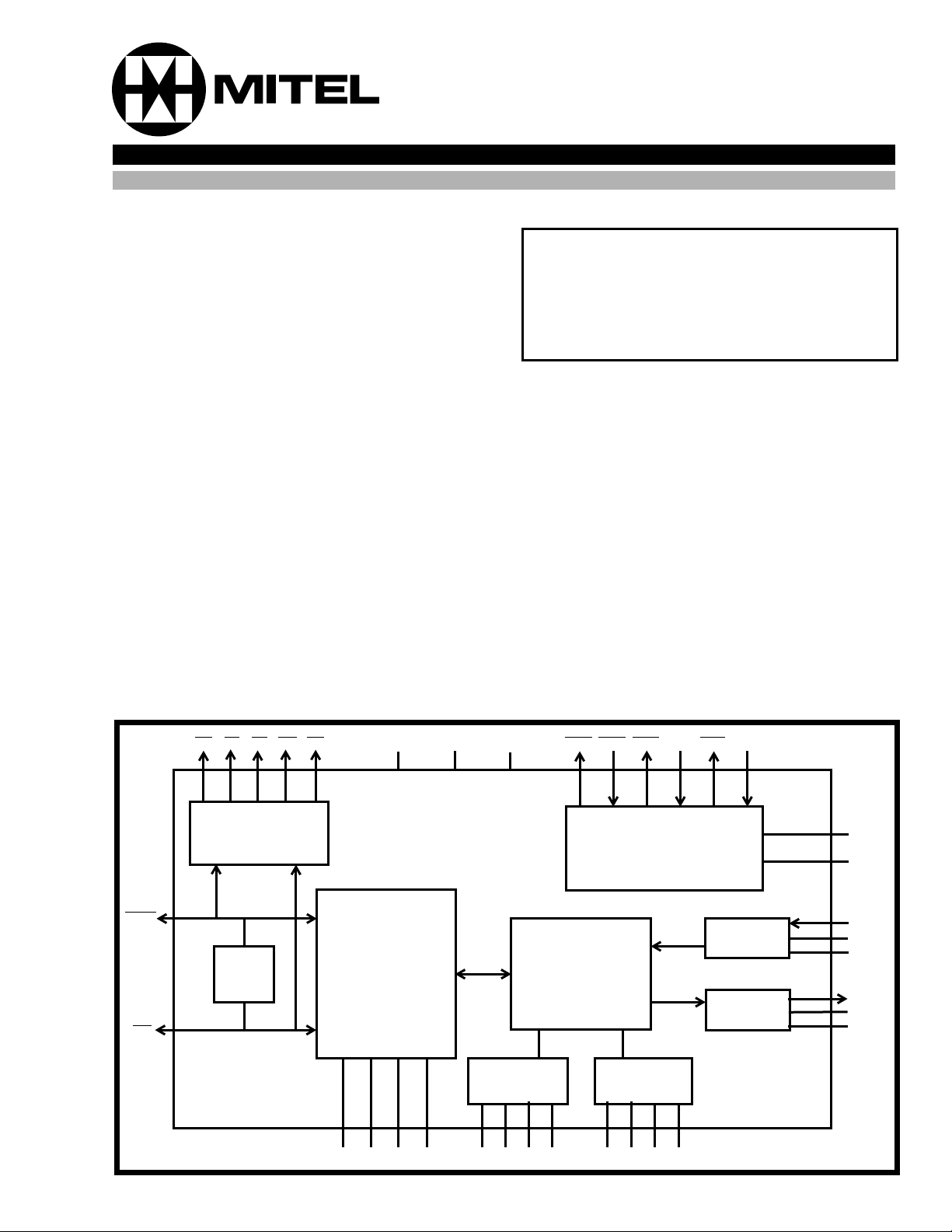
RING
TIP
RV FL RL RG TG
Status
Detection
Dummy
Ringer
VCC VEE AGND
Line
Termination
Impedance
Matching
XLA XLB XLC XLD Z1 Z2 Z600 Z900 NS N1 N2 NATT
GRC
Relay Driver Circuit
2-4 Wire
Hybrid
Network
Balance
Figure 1 - Functional Block Diagram
LRCLRDBRCBRDGRD
Receive
Gain
Transmit
Gain
VRLY
RGND
RX
GRX1
GRX0
TX
GTX1
GTX0
2-239
Page 2
MH88632B Preliminary Information
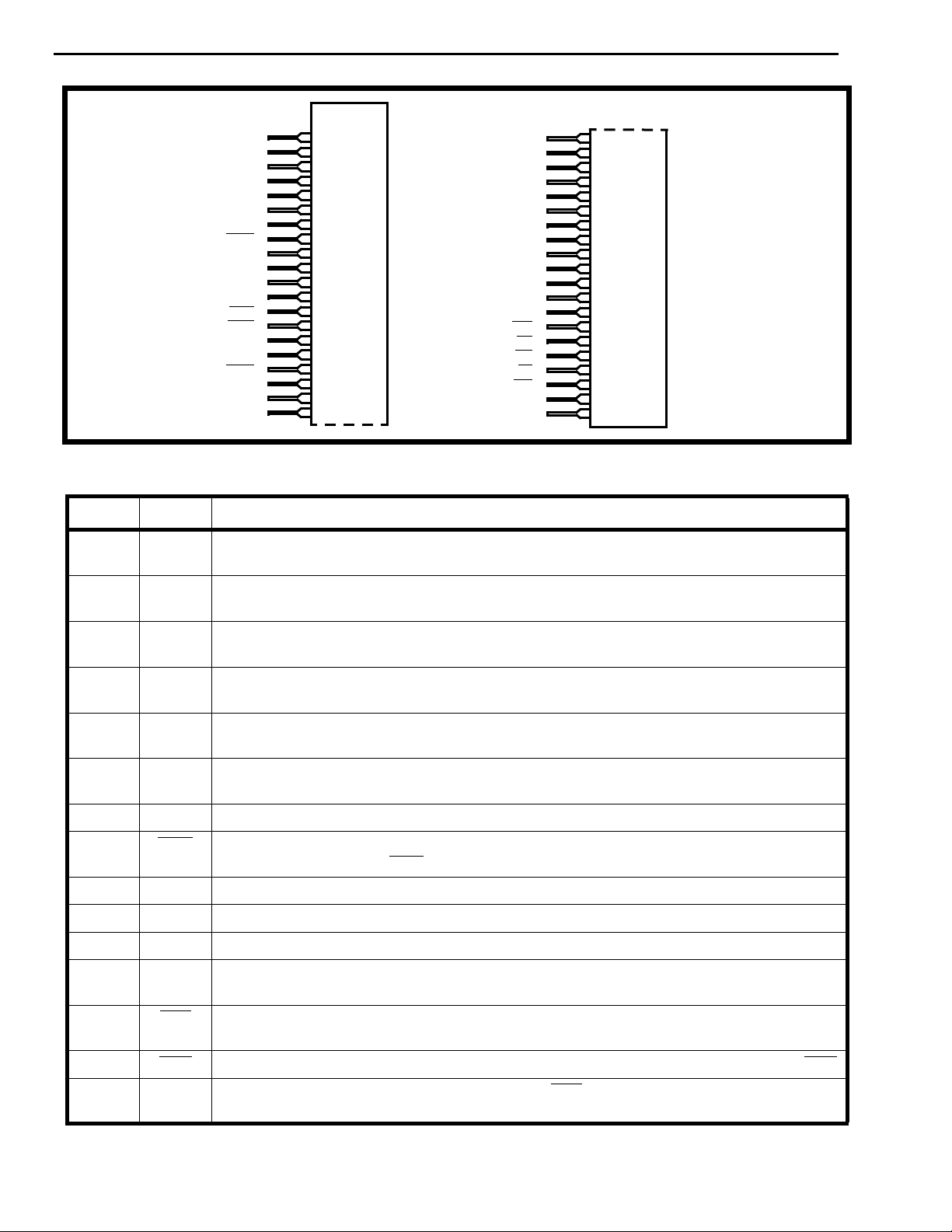
10
11
12
13
14
15
16
17
18
19
20
1
2
3
4
5
6
7
8
9
N2
Z900
Z1
Z2
TX
RX
GTX0
GTX1
GRX0
GRX1
IC
Z600
NS
TG
RL
RV
FL
RG
VEE
VCC
21
22
23
24
25
26
27
28
29
30
31
32
33
34
35
36
37
38
39
40
TIP
RING
XLA
XLB
XLC
XLD
IC
GRD
IC
IC
RGND
VRLY
LRD
BRD
LRC
BRC
GRC
AGND
NATT
N1
Figure 2 - Pin Connections
Pin Description
Pin # Name Description
1 TIP Tip Lead. Connects to the Tip lead of a telephone line usually via an external protection
circuit.
2 RING Ring Lead. Connects to the Ring lead of a telephone line usually via an external protection
circuit.
3 XLA Loop Relay Contact A. Connects to XLB through relay contacts (K1A) when the relay is
energized.
4 XLB Loop Relay Contact B. Connects to XLA through relay contacts (K1A) when the relay is
energized.
5 XLC Loop Relay Contact C. Connects to XLD through relay contacts (K1B) when the relay is
energized.
6 XLD Loop Relay Contact D. Connects to XLC through relay contacts (K1B) when the relay is
energized.
7ICInternal Connection. No connection should be made to this pin.
8 GRD Ground Ring Lead Relay Drive (Output). Connects to the Ground Ring Lead Relay coil
(K3) and is controlled by GRC.
9ICInternal Connection. No connection should be made to this pin.
10 IC Internal Connection. No connection should be made to this pin.
11 RGND Relay Ground. Return path for relay supply voltage.
12 VRLY Relay Positive Supply Voltage. Normally +5V. Connects to all relay coils and the relay
supply voltage.
13 LRD Loop Relay Drive (Output). Connects to the Loop Relay coil (K1) and is controlled by
LRC.
14 BRD Bias Relay Drive (Output). Connects to the Bias Relay coil (K2) and is controlled by BRC.
15 LRC Loop Relay Control (Input). A logic 1 activates LRD. The Loop Relay (K1) is used for
placing the Line Termination across Tip and Ring.
2-240
Page 3

Preliminary Information MH88632B
Pin Description (continued)
16 BRC Bias Relay Control (Input). A logic 1 activates BRD. The Bias Relay (K2) is used to
connect Tip and Ring to -48V via bias resistors. This input should be connected to logic 0
when not used.
17 GRC Ground Ring Relay Control (Input). A logic 0 activates GRD. The Ground Ring Lead
Relay (K3) is used to connect Ring to AGND via a bias resistor. This input should be
connected to logic 1 when not used.
18 AGND Analog Ground. 4-Wire Ground. Normally connects to system ground. This pin must be
connected to the system ground in Ground Start applications.
19 NATT Network Balance AT&T Node. Used when setting the Network Balance Impedance to
AT&T compromise network.
20 N1 Network Balance Node 1. Used when a Network Balance Impedance which differs from
the Input Impedance is required or when NATT is used.
21 N2 Network Balance Node 2. Used when a Network Balance Impedance which differs from
the Input Impedance is required.
22 Z900 Input Impedance 900Ω Node. Connects to Z1 when selecting an Input Impedance of
900Ω.
23 Z1 Input Impedance Node 1. Used when setting the Input Impedance.
24 Z2 Input Impedance Node 2. Used when a user defined Input Impedance is required.
25 TX Transmit (Output). 4-Wire ground (AGND) referenced analog output.
26 RX Receive (Input). 4-Wire ground (AGND) referenced analog input.
27 GTX0 Transmit Gain Node 0. Connects to GTX1 for 0dB transmit gain.
28 GTX1 Transmit Gain Node 1. Connects to GTX0 for 0dB transmit gain or via a resistor to AGND
for transmit gain programming.
29 GRX0 Receive Gain Node 0. Connects to GRX1 for 0dB receive gain.
30 GRX1 Receive Gain Node 1. Connects to GRX0 for 0dB receive gain or via a resistor to AGND
for receive gain programming.
31 IC Internal Connection. No connection should be made to this pin.
32 Z600 Loop Impedance 600Ω Node. Connects to Z1 when selecting an Input Impedance of
600Ω.
33 NS Network Balance Setting (Input). Used to select the Network Balance impedance.
34 TG Tip Lead Ground Detect (Output). A logic 0 output indicates that the Tip lead is at ground
(AGND) potential.
35 RL Reverse Loop Detect (Output). In the on-hook state, a logic 0 output indicates that
reverse loop battery is present. In the off-hook state, a logic 0 output indicates that reverse
loop current is present.
36 RV Ringing Voltage Detect (Output). A logic low indicates that ringing voltage is across the
Tip and Ring leads.
37 FL Forward Loop Detect (Output). In the on-hook state, a logic 0 output indicates that
forward loop battery is present. In the off-hook state, a logic 0 output indicates that forward
loop current is present.
38 RG Ring Lead Ground Detect (Output). A logic 0 output indicates that the Ring lead is at
ground (AGND) potential.
39 VEE Negative Supply Voltage. -5V DC
40 VCC Positive Supply Voltage. +5V DC
2-241
Page 4
MH88632B Preliminary Information
Functional Description
The MH88632B is a Central Office Interface Circuit
(COIC). It is used to correctly terminate a Central
Office 2-Wire telephone line. The device provides a
signalling link and a 2-4 Wire line interface between
the telephone line and subscriber equipment. The
subscriber equipment can include Private Branch
Exchanges (PBX's), Key Telephone Systems,
Terminal Equipment, Digital Loop Carriers and
Wireless Local Loops.
All descriptions assume that the device is connected
as in the application circuit shown in Figure 3.
Isolation Barrier
The MH88632B provides an isolation barrier which is
designed to meet FCC Part 68 (November 1987)
Leakage Current Requirements.
External Protection
An external protection circuit may be required to
assist in preventing overvoltage damage to the
device and the subscriber equipment in which it is
incorporated. The type of protection required is
dependant on the application and the regulatory
standards. Please contact the governing regulatory
body and local approvals testing houses for more
assistance.
This protection is shown in block form in Figure 3.
Suitable Markets
The programmability offered by the MH88632B
enhances its suitability for use throughout the
world. However, care should be taken that all
regulatory requirements, e.g. isolation and DC
termination, are being fulfilled for the particular
application in which the device is intended to be
used.
Line Termination
at a logic 0, the Line Ter mination is removed from
across Tip and Ring.
An internal Dummy Ringer is permanently connected
across Tip and Ring which is a series AC load of
(17kΩ+330nF). This represents a mechanical
telephone ringer and allows ringing voltages to be
sensed. This load can be considered negligible
when the line has been terminated.
Depending on the Network Protocol being used the
line termination can seize the line for an outgoing
call, terminate an incoming call, or if applied and
disconnected at the correct rate can be used to
generate dial pulse signals.
The DC line termination circuitry provides the line
with an active DC load which is equivalent to a DC
resistance of between 190Ω and 290Ω dependant on
the loop current.
AC Input Impedance
The Input Impedance (Zin) is the AC impedance that
the MH88632B places across Tip and Ring in order
to terminate the telephone line. It can be user
defined, set to 600Ω or set to 900Ω.
To select a 600Ω Input Impedance, Z1 should be
connected directly to Z600. No connection should
be made to Z2 or Z900.
To select a 900Ω Input Impedance, Z1 should be
connected directly to Z900. No connection should
be made to Z2 or Z600.
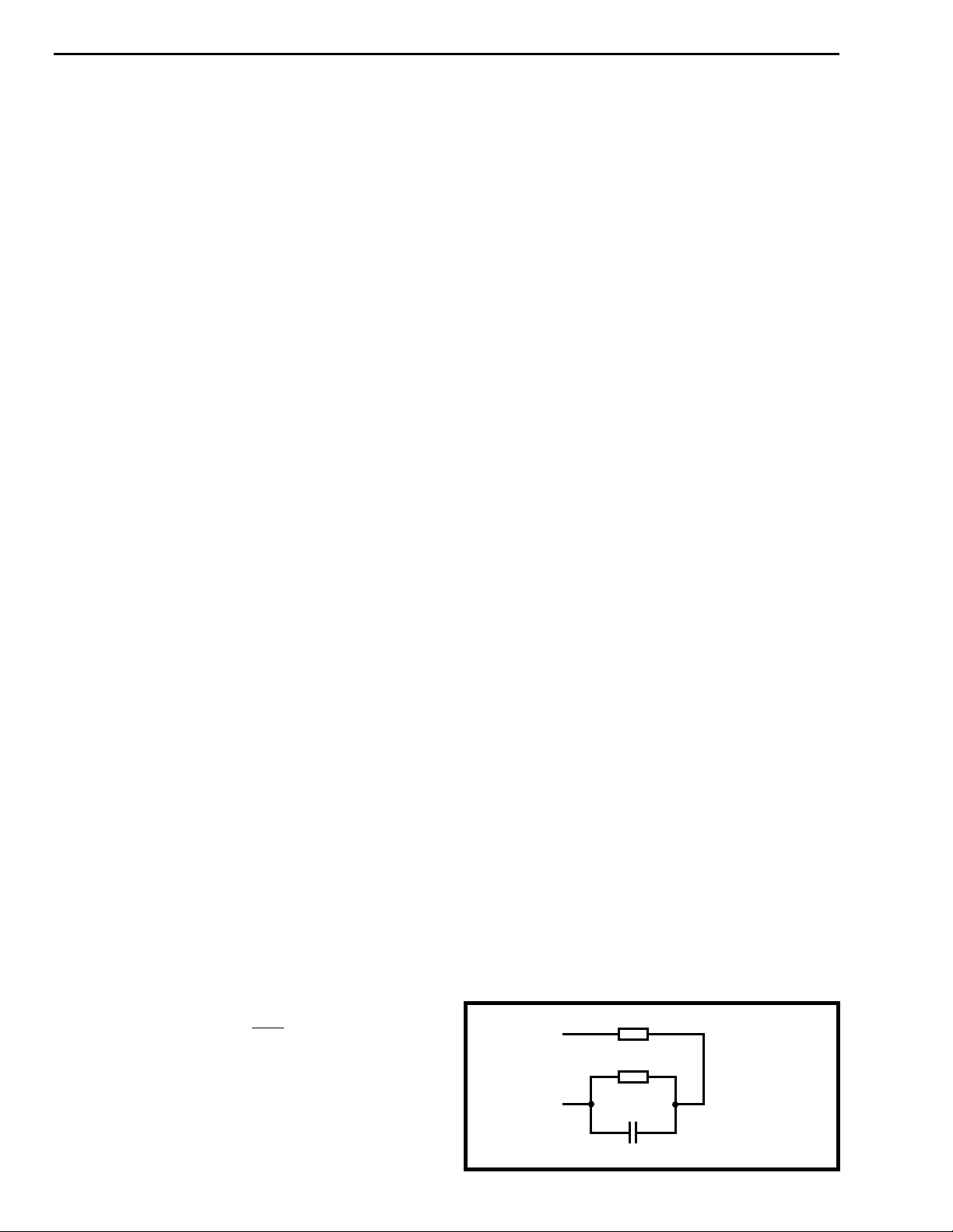
In order to user define the Input Impedance an
impedance network should be placed between Z1
and Z2. This should be equivalent to 10 times the
required Input Impedance and must be greater than
100Ω at 3.4kHz. No connection should be made to
Z600 or Z900.
For example, to implement an Input Impedance of
220Ω+(820Ω//115nF) an impedance network of
2200Ω+(8200Ω//11.5nF) should be connected
between Z1 and Z2 as shown below.
When LRC is at a logic 1, LRD is taken to a logic 0
which energizes the Loop Relay (K1), connecting
XLA to XLB and XLC to XLD. This places a line
termination across Tip and Ring. The device can be
considered to be in an off-hook state and DC loop
current will flow. The line termination consists of a
DC resistance and an AC impedance. When LRC is
2-242
Z1
Z2
2200Ω
8200Ω
11.5nF
Page 5

Preliminary Information MH88632B
User defined Input Impedances can be used to
satisfy most national requirements. See Table 1.
All connections should be kept as short as possible.
Network Balance Impedance
The MH88632B’s Network Balance Impedance can
be selected to mirror the Input Impedance, to be
AT&T compromise or set to a user defined value.
Thus, the Network Balance Impedance can comply
with most national requirements.
With NS at logic 0, the Network Balance Impedance
is selected to mirror the Input Impedance of the
device. No connection should be made to NATT, N1
and N2.
To select a Network Balance Impedance equal to
AT&T Compromise (i.e. 350Ω+(1kΩ//210nF) ), NS
should be set to a logic 1 and a direct connection
made between NATT and N1. No connection should
be made to N2.
The 4-Wire side (TX and RX) can be interfaced to a
filter/codec, such as the Mitel MT896X, for use in
digital voice switched systems.
During full duplex transmission, the signal at Tip and
Ring consists of both the signal from the device to
the line and the signal from the line to the device.
The signal input at RX, being sent to the line, must
not appear at the output TX. In order to prevent this,
the device has an internal cancellation circuit. The
measure of attenuation is Transhybrid Loss (THL).
Programmable Transmit and Receive Gain
The Transmit Gain (GTX) of the MH88632B is the
gain from the balanced signal across Tip and Ring to
the ground referenced signal at TX. It is
programmed by making a connection to GTX1. A
direct connection from GTX1 to GTX0 selects a gain
of 0dB. A direct connection from GTX1 to AGND
selects a gain of +6dB. Other gains can be
programmed by connecting a resistor (RTX) between
GTX1 and AGND. The value of resistor is selected
using the following formulae.
To set a user defined Network Balance Impedance
NS is set to a logic 1. An impedance network which
is 10 times the required Network Balance Impedance
must be placed between N1 and AGND. Another
impedance network must be placed between N1 and
N2 which is 10 times the selected input impedance
of the device.
For example, to implement a Network Balance
Impedance of 220Ω+(820Ω//115nF), an impedance
network of 2200Ω+(8200Ω//11.5nF) must be
connected between N1 and AGND. An impedance
network equal to 10 times the selected Input
Impedance must be connected between N1 and N2.
See Table 2.
All connections should be kept as short as possible.
2-4 Wire Conversion
The device converts the balanced 2-Wire input,
presented by the line at Tip and Ring, to a ground
referenced signal at TX. This circuit operates with or
without loop current; signal reception with no loop
current is required for on-hook reception enabling the
detection of Caller Line Identification signals.
Conversely the device converts the ground
referenced signal input at RX, to a balanced 2-Wire
signal across Tip and Ring.
RTX = 5000
10
GTX = - 20 log(0.5+5000)
R
The Receive Gain (GRX) of the MH88632B is the
gain from the ground referenced signal at RX to the
balanced signal across Tip and Ring. It is
programmed by making a connection to GRX1. A
direct connection from GRX1 to GRX0 selects a gain
of 0dB. A direct connection from GRX1 to AGND
selects a gain of +6dB. Other gains can be
programmed by connecting a resistor (RRX) between
GRX1 and AGND. The value of resistor is selected
using the following formulae.
RRX = 5000
10
GRX = -20 log(0.5+5000)
R
For the correct programming of Transmit and
Receive Gains the selected Input Impedance must
match the specified telephone line characteristic
impedance.
(-GTX/20)
(-GRX/20)
- 0.5
TX
- 0.5
RX
2-243
Page 6

MH88632B Preliminary Information
Both Gains are programmable in the range -12dB to
+6dB. This wide range is capable of accommodating
most system loss plans. See Tables 3 and 4.
Caller Line Identification
Caller Line Identification (CLI) provides the called
party with the calling party telephone number. The
Central Office will utilise the voice path of a regular
loop-start telephone line when the MH88632B is in
the on-hook state. The CLI information is typically a
Frequency Shift Keyed (FSK) data signal which is
output at TX.
Supervisory Features
Line Status Detection Outputs
The MH88632B supervisory circuitry provides the
signalling status outputs which are monitored by the
system controller. The supervisory circuitry is
capable of detecting: ringing voltage; forward and
reverse loop battery; forward and reverse loop
current; grounded tip lead; and grounded ring lead.
If these Supervisory Features and the Control
Features are used as indicated in Figure 3 they can
implement common Network Protocols such as
Loop-Start Signalling and Ground-Star t Signalling.
1. Ringing Voltage Detect Output (RV)
3. Tip Ground and Ring Ground Detect Outputs
(TG & RG)
The TG output provides a logic 0 when the Tip pin is
at ground (AGND) potential.
The RG output provides a logic 0 when the Ring pin
is at ground (AGND) potential.
Control Inputs
The MH88632B accepts control signals from the
system controller at the inputs Loop Relay Control
(LRC), Bias Relay Control (BRC) and Ground Ring
Relay Control (GRC). These energize the relay drive
outputs Loop Relay Drive (LRD), Bias Relay Drive
(BRD) and Ground Ring Relay Drive (GRD)
respectively. Each output is active low and has an
internal clamp diode to VRLY.
The intended use of each of these relay drivers is
shown in Figure 3. LRC is being used to add and
remove the Line Termination from across Tip and
Ring. BRC is used to connect Tip and Ring to -48V
via external bias resistors. GRC is controlling the
connection of Ring to AGND via an external bias
resistor.
If these Control Features and the Supervisory
Features are used as intended they can be used to
implement common Network Protocols such as
Loop-Start Signalling and Ground-Star t Signalling.
The RV output provides a logic 0 when ringing
voltage is detected across Tip and Ring. This
detector includes a filter which ensures that the
output toggles at the ringing cadence and not at the
ringing frequency. Typically this output switches to a
logic 0 after 50ms of applied ringing voltage and
remains at a logic 0 for 50ms after ringing voltage is
removed.
2. Forward Loop and Reverse Loop Detect
Outputs (FL & RL)
The FL output provides a logic 0 when either forward
loop battery or forward loop current is detected, that
is the Ring pin voltage is negative with respect to Tip
pin voltage.
The RL output provides a logic 0 when either reverse
loop battery or reverse loop current is detected, that
is the Tip pin voltage is negative with respect to Ring
pin voltage.
Mechanical Information
See Figure 9 for mechanical specifications for the
MH88632B and Figure 10 for mechanical
specifications for the MH88632BT.
2-244
Page 7

Preliminary Information MH88632B
Tip
Ring
Protection
Circuit
R3
K3
Loop relay Control
Bias Relay Control
Ground Relay Control
+5V
K1
K2
K3
K1A
K1B
R1
R2
13
14
12
11
15
16
17
1
2
8
3
4
5
6
MH88632B
TIP
RING
LRD
BRD
GRD
VRLY
RGND
LRC
BRC
GRC
XLA
XLB
XLC
XLD
K2A
K2B
VCC
GTX1
GTX0
TX
GRX1
GRX0
RX
Z1
Z600
NS
TG
RL
RV
FL
RG
48V Battery
+5V
40
28
27
25
30
29
26
23
32
33
34
35
36
37
38
C1
Analog Out
Analog In
Tip Ground Detect
Reverse Loop Detect
Ringing Voltage Detect
Forward Loop Detect
Ring Ground Detect
NOTES:
1) Configured for 0dB Gain,
and 600Ω Network Balan ce Impedance
2) K1, K2 are E/M FORM C
3) K3 is E/M 1 FORM C
4) R1 = R2 = 30.9kΩ, 1%, 5W
5) R3 = 470Ω, 5%, 5W
6) K2, K3, R1, R2, R3 are required for Ground Start only
7) C1, C2 are decoupling capacitors
600Ω Input Impedance
AGND
18
C2
VEE
39
-5V
Figure 3 - Typical Combined Loop Start and Ground Start Appliation Circuit
2-245
Page 8

MH88632B Preliminary Information
Input Impedance Settings
Z2 Z1 Z600 Z900 Resulting input impedance (Zin)
NA Connect Z1 to Z600 NA 600Ω
NA Connect Z1
to Z900
Connect network from Z1 to Z2 NA NA 0.1 x impedance between Z1 & Z2
Note: NA indicates high impedance (10kΩ) connection to this pin does not effect the resulting Input Impedance
Network Balance Settings
NS (Input) N2 N1 NATT Resulting input impedance (Zin)
Low NA NA NA Equivalent to Zin
High NA Connect N1 to NATT AT&T compromise (350Ω + 1kΩ // 210nF)
High Connect network from N1 to
AGND equivalent to 10 x
NETBAL. Connect network
from N1 to N2 equivalent to 10
x Zin.
Notes: NA indicates high impedance (10kΩ) connection to this pin does not effect the resulting Network Balance Impedance.
Low indicates Logic 0.
High indicates Logic 1.
NA Connect Z1
to Z900
NA
900Ω
Zin must be 600Ω
0.1 x impedance between N1 & N2
Transmit Gain Programming
Transmit
Gain (dB)
+6.0 No Resistor
+4.0 38.3k Results in 0dB overall gain when used with Mitel A-law codec (i.e. MT8967)
+3.7 32.4k Results in 0dB overall gain when used with Mitelµ-law codec (i.e. MT8966)
0.0 GTX0 to GTX1
-3.0 5.49k
-6.0 3.32k
-12.0 1.43k
Note: Overall gain refers to the receive path of PCM to 2-Wire.
RTX Resistor
Value (Ω)
Notes
Receive Gain Programming
Receive
Gain (dB)
+6.0 No Resistor
0.0 GRX0 to GRX1
-3.0 5.49k
-3.7 4.87k Results in 0dB ov er all gain when used with Mitel A-law codec (i.e. MT8967)
-4.0 4.64k Results in 0dB overall gain when used with Mitel µ-law codec (i.e. MT8966)
-6.0 3.32k
-12.0 1.43k
Note: Overall gain refers to the transmit path of 2-wire to PCM.
RRX Resistor
Value (Ω)
Notes
2-246
Page 9

Preliminary Information MH88632B
Absolute Maximum Ratings*
Parameter Sym Min Max Units Comments
1 DC Supply Voltage V
2 DC Relay Voltage V
3 Storage Temperature T
4 Ring Trip Current
*Exceeding these values may cause permanent damage. Functional operation under these conditions is not implied.
V
I
TRIP
CC
EE
RLY
S
Recommended Operating Conditions
Parameter Sym Min Typ
1 DC Supply Voltage V
2 DC Relay Voltage V
3 Operating Temperature T
‡Typical figures are at 25 C with nominal 5V supplies and are for design aid only.
CC
V
EE
RLY
OP
-0.3
0.3
-7
7
V
V
-0.3 20 V
-55 +125 °C
180 mArms 250ms 10% duty cycle or
‡
Max Units Comments
4.75
-4.75
-5
5
5.25
-5.25
V
V
515 V
02570°C
500ms single shot
*
DC Electrical Characteristics
†
Characteristics Sym Min Typ‡Max Units Test Conditions
1 Supply Current I
2 Power Consumption
3 FL
Low Level Output Voltage
RL
High Level Output Voltage
V
V
DD
I
EE
PC
OL
OH
2.4
14
10
15
13
120 147 mW
0.5 V
RG
TG
RV
4 LRD
BRD
Sink Current, Relay to V
Clamp Diode Current
CC
I
OL
I
CD
100
150
GRD
5NS
LRC
Low Level Input Voltage
High Level Input Voltage
V
IL
V
IH
2
0.8 V
BRC
GRC
6NS
LRC
High Level Input Current
Low Level Input Current
I
IH
I
IL
1
1
BRC
GRC
†
Electrical Characteristics are over recommended operating conditions unless otherwise stated.
‡ Typical figures are at 25°C with nominal 5V supplies and are for design aid only.
mA
mA
V
mA
mA
V
µA
µA
IOL = 4mA
IOH= 0.4mA
VOL = 0.35V
2-247
Page 10

MH88632B Preliminary Information
Loop Electrical Characteristics
†
Characteristics Sym Min Typ‡Max Units Test Conditions
1 Ringing Voltage V
R
20 90 130 Vrms
2 Ringing Frequency 17 20 68 Hz
4 Operating Loop Current 15 90 mA
5 Off-Hook DC Resistance 190 275 290 Ω
6 Leakage Current
7 mArms @1000VAC
(Tip-Ring to AGND)
7 FL Threshold
Tip-Ring Voltage Detect (On-hook)
Tip-Ring Current Detect (Off-hook)
12
6
21
12
8 RL Threshold
Tip-Ring Voltage Detect (On-hook)
Tip-Ring Current Detect (Off-hook)
9 TG and RG Detect Threshold
✝Electrical Characteristics are over recommended operating conditions unless otherwise stated.
‡Typical figures are at 25°C with nominal 5V supplies and are for design aid only.
AC Electrical Characteristics
†
Characteristics Sym Min Typ
1 2-wire Input Impedance
Zin 600
-12
-6
-12
-21
-12
-14 V
‡
Max Units Test Conditions
900
2 Return Loss at 2-Wire
(Zin = 600Ω)
3 Return Loss at 2-Wire
(Zin = 900Ω)
Note 1
RL
20
26
20
RL 22
26
Ext.
40
48
46
24
4 Longitudinal to Metallic Balance
Note 2
58
58
55
53
51
64
63
61
57
54
5 Metallic to Longitudinal Balance
6 Transhybrid Loss
(Zin = Net = 600Ω) Note 2 & 3
7 Transhybrid Loss
(Zin = Net = 900Ω) Note 2 & 3
8 Transhybrid Loss
(Zin =600Ω, Net = AT&T) Note 2 & 3
Note 2
60
40
THL 18
21
THL 18
21
THL 18
21 30
62
62
25
33
9 Input Impedance At RX 10 kΩ
10 Output Impedance at TX 5 Ω
11 Transmit Gain, (2-Wire/TX):
Default Gain(0dB)
Programmable Range
-0.2
-12 0
0.2
6
V
mA
V
mA
LRC = 0V
LRC = 5V
LRC = 0V
LRC = 5V
Ω
Ω
Ω
Test Circuit Fig. 6
dB
dB
dB
dB
dB
dB
200-500 Hz
500-1000 Hz
1000-3400 Hz
200-500 Hz
500-1000 Hz
1000-3400 Hz
Test Circuit Fig. 8
dB
dB
dB
dB
dB
200 Hz
1000 Hz
2000 Hz
3000 Hz
4000 Hz
Test Circuit Fig. 7
dB
dB
200-1000 Hz
1000 -4000 Hz
dBdB200-3400 Hz
500-2500 Hz
dBdB200-3400 Hz
500 -2500 Hz
dBdB200-3400 Hz
500-2500 Hz
Test Circuit Fig. 5
dB
dB
Input 0.5V
1000Hz
1000Hz
2-248
Page 11

Preliminary Information MH88632B
AC Electrical Characteristics† (continued)
Characteristics Sym Min Typ‡Max Units Test Conditions
12 Frequency response gain
(relative to gain at 1kHz)
13 Receive Gain, (RX/2-Wire):
Default Gain (0dB)
Note 2 -1.3
-0.3
-0.3
-0.7
-0.2
0
0
0
0
0.1
0.1
0.1
0.1
0 0.2
dB
dB
dB
dB
dB
Test Circuit Fig. 5
Input 0.5V
200 Hz
300 Hz
3000 Hz
3400 Hz
Test Circuit Fig. 4
Input 0.5V
1000Hz
Programmable Range
14 Frequency response gain
(relative to gain at 1kHz)
15 Signal Output Overload Level
16 Total Harmonic Distortion
17 Idle Channel Noise
Note 2 -1.3
at 2-wire
at TX
THD
at 2-Wire
at TX
Nc
at 2-Wire
at TX
-12
-0.3
-0.3
-0.7
4
4
0
0
0
0
0.2
0.4
10
11
6
0.1
0.1
0.1
0.1
1
1
13
13
dB
dB
dB
dB
dB
dBm
dBm
%
%
dBrn
C
1000Hz
Test Circuit Fig. 4
Input 0.5V
200 Hz
300 Hz
3000 Hz
3400 Hz
THD < 5%
Ref. 600Ω
Ref. 600Ω
Input 0.5V, 1kHz
dBrn
C
18 Common Mode Rejection Ratio CMRR 48 65 dB 540Hz
Test Circuit Fig. 8
19 Power Supply Rejection Ratio
PSRR
Ripple 0.1V, 1kHz
at 2-Wire and TX
V
CC
V
EE
20
20
42
28
dB
dB
20 On-Hook Transmit Gain (2-Wire/TX)
Default Gain 0dB
-1
01
1000Hz
Programmable Range
21 On-Hook frequency Response
-12
6dBdB
-1 0 1 dB Input 0.5V, 1kHz
Gain (relative to off-hook gain)
✝Electrical Characteristics are over recommended operating conditions unless otherwise stated
‡Typical figure are at 25°C with nominal 5V supplies and are for design aid only
*All test conditions use a test source impedance which matches the device’s input impedance
dBm is referenced to 600Ω unless otherwise stated
Notes: Impedance set by external network equal to 10 times the required input impedance
Test conditions use a transmit and receive gain set to 0dB default
"Net" indicates network balance impedance
1000Hz
2-249
Page 12

MH88632B Preliminary Information
Z1
Z600
GRX0
GRX1
GTX0
GTX1
TX
RX
Gain = 20 x Log (Vtx/Vs)
+5V
VCC
-5V
VEE
AGNDNS
RING
XLA
XLB
XLC
XLD
TIP
I = 15mA
-V
10H 650Ω
10H 650Ω
Figure 4 - 2-4 Wire Gain Test Circuit
100µF
+
~
+
100µF
Vs = 0.5V
600Ω
Vs = 0.5V
~
+5V
VCC
Z1
Z600
GRX0
GRX1
GTX0
GTX1
TX
RX
Gain = 20 x Log (Vz/Vs)
Figure 5 - 4-2 Wire Test Circuit
-5V
VEE
AGNDNS
RING
XLA
XLB
XLC
XLD
TIP
I = 15mA
-V
10H 650Ω
100µF
+
Z = 600Ω
+
100uF
10H 650Ω
2-250
Page 13

Preliminary Information MH88632B
Z1
Z600
GRX0
GRX1
GTX0
GTX1
TX
RX
Return Loss = 20 x Log (V1\Vs)
+5V
VCC
-5V
VEE
AGNDNS
RING
XLA
XLB
XLC
XLD
TIP
I = 15mA
-V
Figure 6 - Return Loss Test Circuit
10H 650Ω
100µF
+
V1
+
100µF
10H 650Ω
600Ω
368Ω
~
368Ω
Vs = 0.5V
+5V
VCC
Z1
Z600
GRX0
GRX1
GTX0
GTX1
TX
RX
Met to Long. Balance = 20 x Log (V1/Vs)
-5V
VEE
Figure 7 - Metallic to Longitudinal Balance Test Circuit
-V
10H 650Ω
100µF
RING
AGNDNS
I = 15mA
XLA
XLB
XLC
XLD
TIP
+
510Ω
+
100µF
10H 650Ω
V1
368Ω
368Ω
~
Vs = 0.5V
2-251
Page 14

MH88632B Preliminary Information
+5V
VCC
Z1
Z600
GRX0
GRX1
GTX0
GTX1
TX
RX
Long. to Met. Balance = 20 * Log (V1/Vs)
CMRR = 20 * Log (Vtx/Vs)
-5V
VEE
AGNDNS
RING
XLA
XLB
XLC
XLD
TIP
I = 15mA
-V
10H 650Ω
10H 650Ω
100µF
+
+
100µF
V1
368Ω
368Ω
Vs = 0.5V
~
Figure 8 - Longitudinal to Metallic Balance and CMRR Test Circuit
1
0.125 Max
(3.18 Max)
Notes:
1) Not to scale
2) Dimensions in inches.
(Dimensions in millimetres)
3) Pin tolerances are non-accumulative.
4) Recommended soldering conditions:
Wave Soldering -
Max temp at pins 260˚ for 10 secs.
* Dimensions to centre of pin.
0.125 Max
(3.18 Max)
0.010 +0.002
(0.25 +0.05)
4.23 Max
(107.5 Max)
0.64 +0.02
(16.25 +5.1)
1
*
0.250 +0.020
(6.35 +0.51)
*
0.100
(2.54 +0.25)
+0.010
0.180 +0.020
+0.51)
(4.57
0.020 +0.005
(0.5
+0.13)
2-252
Figure 9 - MH88632B Mechanical Information
Page 15

Preliminary Information MH88632B
4.23 Max
(107.5 Max)
0.62 Max
(15.75 Max)
1
0.080
+0.020
(2.03 +0.51)
0.170 Max
(4.32 Max)
Notes:
1) No t to scale
2) Dimensions in inches.
(Dimensions in millimetres)
3) Pin tolerances are non-accumulative.
4) Recommended soldering conditions:
Wave Soldering Max temp at pins 260˚ for 10 secs.
* Dimensions to centre of pin.
Figure 10 - MH88632BT Mechanical Information
0.260 +0.015
+0.38)
(6.60
*
0.250 +0.020
+0.51)
(6.35
*
0.100 +0.010
(2.54 +0.25)
0.020 +0.005
(0.51
+0.13)
0.080 Max
(2.03 Max)
2-253
Page 16

MH88632B Preliminary Information
Notes:
2-254
Page 17

http://www.mitelsemi.com
World Headquarters - Canada
Tel: +1 (613) 592 2122
Fax: +1 (613) 592 6909
North America Asia/Pacific Europe, Middle East,
Tel: +1 (770) 486 0194 Tel: +65 333 6193 and Africa (EMEA)
Fax: +1 (770) 631 8213 Fax: +65 333 6192 Tel: +44 (0) 1793 518528
Fax: +44 (0) 1793 518581
Information relating to products and services furnished herein by Mitel Corporation or its subsidiaries (collectively “Mitel”) is believed to be reliable. However, Mitel assumes no
liability for errors that may appear in this publication, or for liability otherwise arising from the application or use of any such information, product or service or for any infringement of
patents or other intellectual property rights owned by third parties which may result from such application or use. Neither the supply of such information or purchase of product or
service conveys any license, either express or implied, under patents or other intellectual property rights owned by Mitel or licensed from third parties by Mitel, whatsoever.
Purchasers of products are also hereby notified that the use of product in certain ways or in combination with Mitel, or non-Mitel furnished goods or services may infringe patents or
other intellectual property rights owned by Mitel.
This publication is issued to provide information only and (unless agreed by Mitel in writing) may not be used, applied or reproduced for any purpose nor form part of any order or
contract nor to be regarded as a representation relating to the products or services concerned. The products, their specifications, services and other information appearing in this
publication are subject to change by Mitel without notice. No warranty or guarantee express or implied is made regarding the capability, performance or suitability of any product or
service. Information concerning possible methods of use is provided as a guide only and does not constitute any guarantee that such methods of use will be satisfactory in a specific
piece of equipment. It is the user’s responsibility to fully determine the performance and suitability of any equipment using such information and to ensure that any publication or
data used is up to date and has not been superseded. Manufacturing does not necessarily include testing of all functions or parameters. These products are not suitable for use in
any medical products whose failure to perform may result in significant injury or death to the user. All products and materials are sold and services provided subject to Mitel’s
conditions of sale which are available on request.
M Mitel (design) and ST-BUS are registered trademarks of MITEL Corporation
Mitel Semiconductor is an ISO 9001 Registered Company
Copyright 1999 MITEL Corporation
All Rights Reserved
Printed in CANADA
TECHNICAL DOCUMENTATION - NOT FOR RESALE
 Loading...