

Page 1
2-157
Features
• Fully programmable line impedance,network
balance impedance and gains
• Programmable loop current with long loop
capability
• 2-4 Wire conversion
• Power down and wake up
• Battery feed to line with wide operating range
• Off-hook and dial pulse detection
• Over-current protection
• Integral ringing amplifier with auto ring trip
• Tip/Ring reversal
• Meter pulse injection
• On-hook transmission to the line capability
• Relay driver
• Short loop ringing capability with low voltage
DC supply
Applications
Line interface for:
• PABX/Key Telephone System
• Analog Terminal Adaptors
• Pair Gain System
• Fibre in the Loop/Wireless Local Loop
Description
The Mitel MH88617 is a highly featured, low cost
Subscriber Line Interface Circuit (SLIC). It provides a
total analog transmission and signalling link between
a CODEC and a subscriber line. All functions are
integrated into a single thick film hybrid module,
which provides high reliability and optimum circuit
design needing a minimum of external components.
The line impedance, network balance impedance,
gain and loop current are all externally
programmable, making the device suitable for a wide
range of applications worldwide.
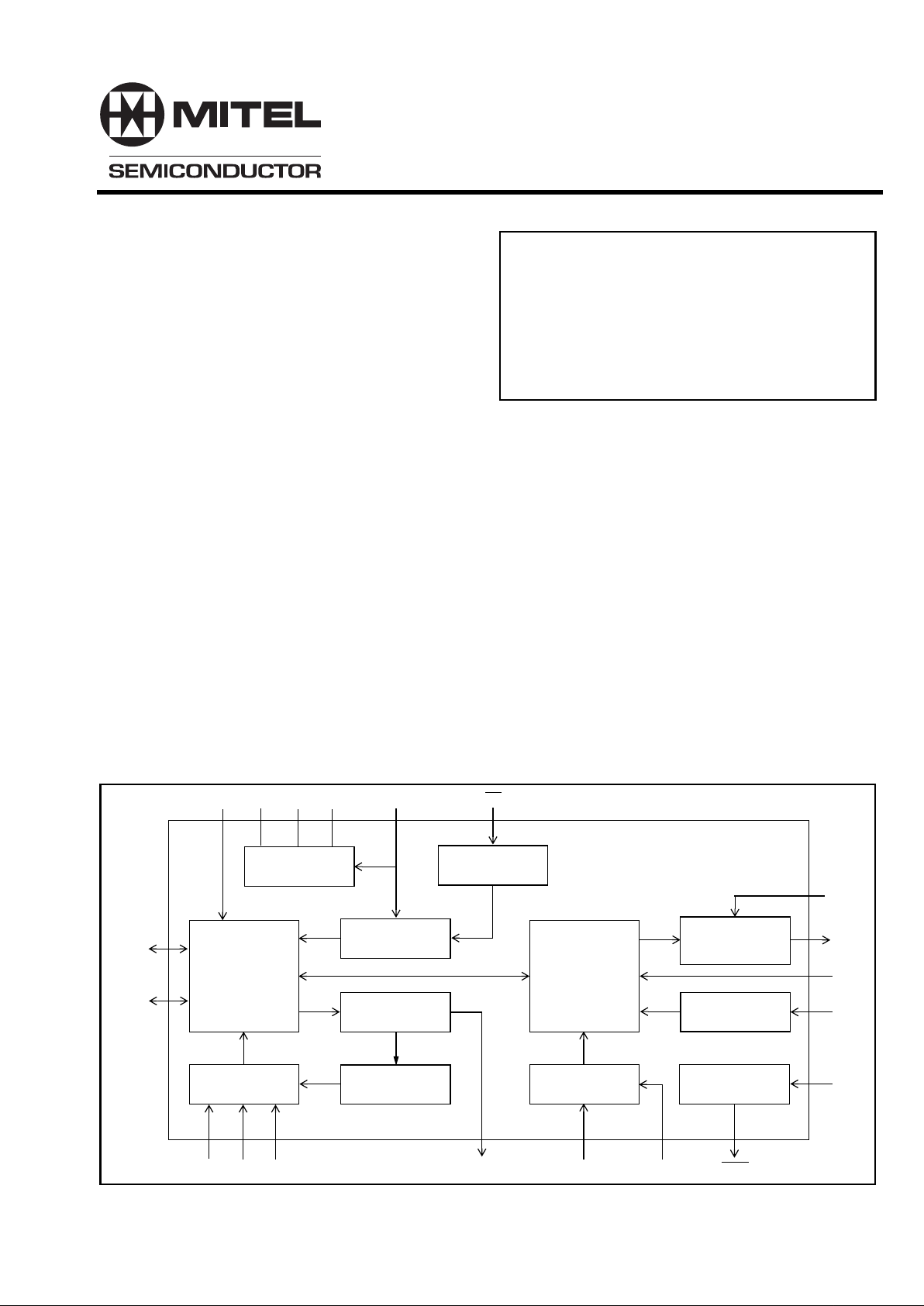
Figure 1 - Functional Block Diagram
TIP
RING
GVX
VBAT VCC VEE GND LCA
Ringing Control
and
Amplifier
LR
Power
Management
Constant
Current Control
Reversal
Supervision
Auto Ring Trip
TIP / RING
Drive and
Sense
VX
VR
ZA
RDI
RDOESEESISHKDCRI
RV
RC
2 - 4 Wire
Conversion
Gain Adjust
Programmable
Impedance
Metering
Injection
Relay Driver
& Programmable
Network Balance
DS5037 ISSUE 4 May 1999
Ordering Information
MH88617AV-PI 21PIN SIL Package
MH88617AD-PI 28PIN DIL Package
MH88617AS-PI 28PIN SM Package
MH88617AT-PI 21PIN 90° L/F Package
-40°C to 85°C
MH88617
Programmable SLIC with Ringing Amplification
Advance Information
Page 2
MH88617 Advance Information
2-158
Figure 2 - Pin Connections
Pin Description
28
Pin
DIL
21
Pin
SIL
Name Description
26 1 DCRI DC Ringing V olta ge Input. A continuous DC voltage is applied to this pin. This voltage
is the positive supply rail for the internal ringing amplifier.
16 2 RDI Relay Driver Input. Relay driver control pin.
15 3 RDO Relay Driver Output. Open collector relay driver output.
54LR Line Reversal. Setting this pin to a logic 0 will perform a line reversal. This pin must be
connected to logic 1 for normal operation.
1 5 TIP Tip Lead. Connects to the "Tip" lead of the subscriber line.
3 6 RING Ring Lead. Connects to the "Ring" lead of the subscriber line.
12 7 VBAT Battery Voltage. Battery supply for the subscriber line. Typically -48V DC is applied to
this pin.
9 8 LCA Loop Current Adjust. The loop current is programmed by connecting a resistor between
this pin and the VCC or AGND pins. Leaving this pin open circuit def aults the loop current
to 24mA. Setting this pin to 0V will apply power down.
28 9 VX Transmit Signal (Output). 4-wire analog signal from the SLIC.
27 10 GVX Transmit Gain Adjust. The transmit gain can be programmed by connecting a resistor
between this pin and VX. The Network Balance Impedance can also be programmed by
connecting external matching components from this pin to VR.
17 11 VR Receive Signal (Input). 4-wire analog signal to the SLIC.
22 12 VCC Positive Supply Voltage. +5V.
21 13 AGND Analog Ground. Ground path for the subscriber line and all DC power supplies,
normally connected to system ground.
20 14 VEE Negative Supply Voltage. -5V.
1
2
3
4
5
6
7
8
9
10
11
12
13
14
15
16
17
18
19
20
21
DCRI
RDI
RDO
LR
TIP
RING
VBAT
LCA
VX
GVX
VR
VCC
AGND
VEE
RV
ESE
ESI
IC
SHK
RC
ZA
21 Pin SIL
28 Pin DIL
1
2
3
4
5
6
7
8
9
10
11
12
13
14 15
16
17
18
19
20
21
22
23
24
25
26
27
28
TIP
IC
RING
IC
LR
RC
ESE
ESI
LCA
IC
IC
VBAT
IC
SHK
VX
GVX
DCRI
IC
IC
IC
VCC
AGND
VEE
RDO
RDI
VR
RV
ZA
Page 3

Advance Information MH88617
2-159
18 15 RV Ringing Voltage. A low level AC sinusoid is applied to this pin. This signal is amplified
and output from TIP/RING to the line as the ringing signal, when RC is at logic 1. This pin
should be driven with a low impedance AGND centred source.
7 16 ESE External Signal Enable. Meter pulse input enable.
8 17 ESI External Signal Input. Meter pulse input.
2,
4,10
11,13
,23
25,24
18 IC Internal Connection. No connection should be made to this pin.
14 19 SHK Switch Hook Detect (Output). A logic 1 at this pin indicates when the subscriber has
gone Off-Hook.
620RCRinging Control (Input). A logic 1 will cause the ringing voltage to be applied to the line.
19 21 ZA Line Impedance. Connect passive components from ZA to ground to match input and
line impedance.
Pin Description (continued)
28
Pin
DIL
21
Pin
SIL
Name Description
Functional Description
The MH88617 is a Subscriber Line Interface Circuit
(SLIC) used to provide an analog interface between
the 4-wire connection and the 2-wire subscriber line
of a communications system.
It provides powering of the subscriber line along with
signalling, control and status circuits. This combines
to provide a comprehensive line and interface
solution in applications such as PABX, Key Systems,
Analog Terminal Adapters, Pair Gain Systems, Fibre
in the Loop and Wireless Local Loop.
External Protection Circuit
An External Protection Circuit assists in preventing
damage to the device and the subscriber equipment,
due to over-voltage conditions (see Figure 3). Also
reference MSAN-156.
2-4 Wire Conversion
The SLIC converts the balanced 2-Wire input at Tip
and Ring to a ground referenced signal at VX. The
device converts the ground referenced signal input at
VR to a balanced 2-Wire signal across Tip and Ring.
Normally the VX and VR pins connect to a Codec
that interfaces the analog signal to a digital
network.During full duplex transmission, the signal at
Tip and Ring consists of both the signal from the
device to the line and the signal from the line to the
device. The signal input at VR being sent to the line,
must not appear at the output VX. In order to prevent
this, the device has an internal cancellation circuit,
the measure of this attenuation is Transhybrid Loss
(THL).
The MH88617 has the ability to transmit analog
signals from VR through to Tip and Ring when onhook. This can be used when sending caller line
identification information.
Battery Feed and Loop Current Adjust
The MH88617 has an active feedback circuit to
regulate the DC current to the subscriber line. This
current is programmable over a wide range via the
LCA pin. With LCA open circuit the current will be set
to 24mA. This can be increased up to 55mA by
connecting a resistor between LCA and VCC or
reduced down to 14mA by connecting a resistor
between LCA and AGND. MSAN-156 shows a table
of resistor values and loop current.
The line driver stage is biased between +5V and
-48V DC. Therefore it should be noted that loop
current will flow in the +5V supply, this must be taken
into consideration when choosing the +5V supply.
The device will operate over a very wide VBAT
supply range but care must be taken when
programming the constant current that the maximum
power dissipation is not exceeded. For the major ity
Page 4
MH88617 Advance Information
2-160
of applications this will not be a problem, however
the device could be damaged if used to drive a very
short line with the maximum battery voltage and
maximum programmable loop current.
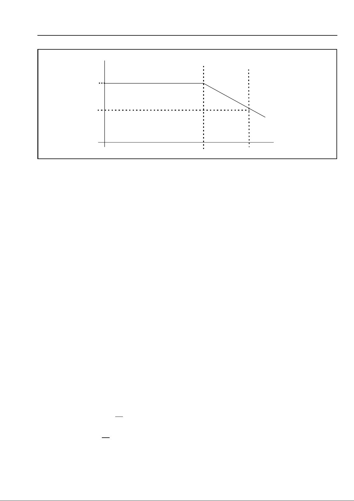
For very long loops the constant current drive reverts
to a constant voltage source. A graph of loop current
versus line resistance is shown in Figure 4.
Under fault conditions, Tip or Ring are protected
from short circuits to ground when the current
exceeds the protection trip threshold. Under these
circumstances, the SLIC will go into a power down
mode and periodically check the line status until the
fault has been removed. Thereby minimizing power
dissipation. The SLIC will revert to an operational
state once the fault is removed.
Ringing Amplification
The MH88617 incorporates an internal ringing
amplifier circuit. A balanced ringing signal is applied
across Tip and Ring, when a DC voltage is
connected to the DCRI pin, a low level sinusoidal
signal is applied to RV and RC is set to logic 1. The
ringing voltage is approximately 50 times the signal
at RV. The gain depends on the ringer load and
impedance at ZA. If an absolute gain is required, a
transistor can be fitted across ZA to give 42.
The SLIC also has the ability to provide ringing on
short loops without the need for a high voltage DCRI
supply. This is achieved by connecting the DCRI pin
to a low voltage supply such as +5V or +12V
providing the subscriber equipment ringing detector
has a low enough sensitivity threshold. In this
application the input at RV needs to be a square
wave (refer MSAN-156).
The SLIC has an automatic ring-trip circuit that
ensures the ringing is removed when the subscriber
goes off-hook. However the user must still insure RC
is taken to logic 0 when SHK signals the subscriber
has gone off-hook.
Programmable Input Impedance
By connecting external passive components
between ZA and ground (AGND) the device’s input
impedance can be set to match the line impedance.
As shown in Figure 3 and Table 1. A more
comprehensive list is given in MSAN-156.
Programmable Network Balance
The network balance of the device can be
programmed by connecting external passive
components between GVX and VR, as shown in
Figure 3 and Table 1.
Figure 3 - Typical Application Circuit
TIP
RING
VX
VR
AGND
VCC
TIP
RING
+5V
MH88617
Protection
Circuit
Notes:
ZA
Z1
VEE VBAT DCRI
-5V
-48V
RV
LR
GVX
SD3
SD2
SD1
SD0
RDI
ESE
RC
VX
VR
MT896x
ESI
SHK
RDO
SHK
Relay Drive
Output
LCA
Loop Current
Adjust Input
1.0Vrms
Sinewave
(16-68Hz)
1.0Vrms
Sinewave
(12/16kHz)
1) For Resistor and Impedance values
0-100V
DSTo
DSTi
CLK
F1i
CA
+5V
10k
C1 C2
2) C1 and C2 are 100nF decoupling capacitors
R2
Z2
R1
see Table 1
T
E.G Teccor
P2353AB
F1
F2
3) F1 and F2 Slow Blow Fuses
Page 5
Advance Information MH88617
2-161
Table 1 gives table of values for some common
applications. A more comprehensive list is given in
MSAN-156.
Programmable Transmit and Receive
Gain
The transmit gain from Tip and Ring to VX can be
programmed by connecting a resistor between GVX
and VX. Similarly the Receive Gain from VR to Tip
and Ring can be programmed by connecting an
impedance in series with VR as shown in Figure 3
and Table 1. Refer to MSAN-156 for additional
impedances.
Off-Hook and Dial Pulse Detection
The switch hook detect output (SHK) goes to a logic
1, when loop current is above the detect threshold
(see DC Electrical Characteristics). This occurs
when the subscriber’s equipment seizes the line to
initiate a call or answer a call. When loop disconnect
dialling is being used, SHK pulses to logic 0 to
indicate the digits being dialled. This output should
be debounced by the system software.
During On-hook transmission SHK remains at logic
0.
Reversal
During normal operation i.e. LR connected to logic 1,
the DC voltage on Tip is positive with respect to
Ring. This can be reversed by applying a logic 0 to
the Line Reversal pin (LR). This feature is used for
signalling. The SLIC is functional during reversal but
for optimum performance forward operation is
recommended.
Meter-Pulse Injection
If the External Signal Enable (ESE) is taken to logic
1 and a 12kHz or 16kHz Meter Pulse signal is
applied to the ESI pin then this signal will be
amplified and output across Tip and Ring. This is
used for calculating the cost of a telephone call.
The gain of the meter pulse signal varies with
programmed input impedance e.g. with the input
impedance programmed for 600Ω and a 200Ω AC
load applied across Tip and Ring the ESI signal will
be amplified by a factor of 2.
Some applications require the 12/16 kHz meter
pulse signal to be ramped before being input at ESI.
Power Down
If AGND is applied to LCA pin the MH88617 will
enter a power down mode where the internal circuitry
is turned off and the power consumption is reduced.
This can be used to conserve power when the line is
inactive.
If the system wants to initiate a call the AGND must
be removed from the LCA before the ringing signal is
transmitted.
If the subscriber initiates a call by seizing the line, SHK
will go to logic 1. The system should monitor this and
respond by removing the AGND from LCA causing the
device to wake up.
Figure 4 - Loop Current vs. Line Resistance
24mA
0Ω
≈1800Ω
R
LOOP
I
LOOP
VBAT @ -48V
LCA O/C
Constant
Current
Constant
Voltage
≈2800Ω
14mA
Page 6

MH88617 Advance Information
2-162
Relay Driver
An open collector output is provided as a driver for
an external relay. Applying 5V to the RDI pin will
cause the RDO pin to sink current to ground. A
flyback diode must be connected across the relay
coil to protect this output.
The DC resistance of the relay coil must exceed
230Ω
Mechanical Data
See Figure 11, 12, 13, and 14 for details of the
mechanical specification.
Table 1 - External Programming Components
Note: The programming component values shown, give the optimum performance in terms of gain accuracy, return loss and THL. A
compromise is these values can be made if a reduction in performance is acceptable.
Line Conditions Programming Components
Line
Impedance
Balance
ImpedanceVXGainVRGain
Z1 Z2 R1 R2
600Ω 600Ω 0dB 0dB 30k 18k + 18k T
470pF
36k 110k
600Ω 600Ω 4dB -4dB 30k 28k5 + 28k5 T
330pF
57k 180k
600Ω 350Ω+1KΩ
//210nF
0dB 0dB 60k//30k 18k + 18k T
(10k3+5.3nF)
36k 110k
370Ω+620Ω/
/310nF
370Ω+620Ω
//310nF
0dB 0dB 40k//(1.2nF+ 32k5) 18k + 18k T
100pF
36k (124k//1.5nF)
+ 64k
220Ω+820Ω/
/115nF
220Ω+820Ω
//115nF
0dB 0dB 41k//(630pF+3k) 36k 36k (164k//550pF)
+ 34k
900Ω 900Ω 0dB 0dB 38k9 18k+18k T
330pF
36k 174k
270Ω+750Ω/
/150nF
270Ω+750Ω
//150nF
0dB 0dB 40k3//(11k5+730pF) 18k+18k T
100pF
36k (150k//760pF)
+ 48k5
Page 7

Advance Information MH88617
2-163
*Exceeding these values may cause permanent damage. Functional operation under these conditions is not implied.
.
‡ Typical figures are at 25˚C with nominal supply voltages and are for design aid only
Note 1: Applies to a sinusoidal input. RV can also be driven with a TTL signal (AC coupled) see MSAN-156.
Absolute Maximum Ratings* - All voltages are with respect to AGND unless otherwise specified.
Parameter Sym Min Max Units
1 DC Supply Voltage V
CC
V
EE
-0.3
-6
6
0.3
V
V
2 DC Battery Voltage V
BAT
-75 0.3 V
3 DC Ringing Voltage V
DCRI
-0.7 150 V
4 DC Reference Voltage LCA -0.3 6 V
5 Relay Driver Voltage RDO -0.3 15 V
6 Relay Driver Coil Resistance 230 Ω
7 Ringing Input Voltage RV 0 3 Vrms
Note 1
8 Maximum Power Handling Capacity
(Off-hook) @ 25˚C
@ 70˚C
@ 85˚C
PD 2250
1530
1290
mW
mW
mW
9 Storage Temperature T
S
-55 +125 ˚C
Recommended Operating Conditions
Parameter Sym Min Typ‡Max Units Test Conditions
1 DC Supply Voltages V
CC
V
EE
4.75
-5.25
5.0
-5.0
5.25
-4.75
V
V
2 DC Battery Voltage V
BAT
-72 -48 -20 V
3 DC Ringing Voltage V
DCRI
5 110 V
4 Ringing Input Voltage RV 2.5 Vrms Note 1
5 Ringing Output Power PR 2250 mW @ 25˚C
6 Operating Temperatures T
OP
-40 25 85 ˚C
Page 8

MH88617 Advance Information
2-164
† Electrical Characteristics are over Recommended Operating Conditions unless otherwise stated.
‡Typical figures are at 25°C with nominal supply voltages and are for design aid only.
Note: Figure quoted is the +5V supply current plus loop current which flows between -48V (battery supply) and the +5V supply
DC Electrical Characteristics
†
Characteristics Sym Min Typ
‡
Max Units Test Conditions
1 Supply Current
I
CC
I
CC
I
EE
I
BAT
I
DCRI
I
DCRI
12
I
Loop
+ 12
-12
-3
100
100
mA
mA
mA
mA
µA
mA
Test circuit as Fig 7
On-Hook
Off-Hook Note
On-Hook
On-Hook
RC at logic 0
RC at logic 1
2 Power Consumption PC 40
270
80 mWmWPower down,
On-hook = -48V
Idle
3 Constant current feed to line I
Loop
24 mA LCA O/C, V
bat
= -48V
R
Loop
= 300Ω, VCC= 5V
4 Adjustable loop current range I
Loop
14 55 mA
5 Maximum operating loop
resistance
R
Loop
2000 Ω I
Loop
= 18mA,
V
bat
= -48V
includes telephone set
6 Tip or Ring to Gnd, Over-
Current Protection
100 mA V
bat
= -48V
7 Low Level Output Voltage
High Level Output Voltage
V
OL
V
OH
2.4
0.4 V
V
IOL= 4mA
IOH= 0.4mA
8 Relay driver current sink
capability
20 mA RDI = 5V
9 Low Level Input Voltage
High Level Input Voltage
Low Level Input Current
High Level Input Current
V
IL
V
IH
I
IL
I
IH
5.0
0.1
0.5
0.8 V
V
mA
mA
10 Switch Hook detect threshold 4 8.5 13 mA V
bat
= -48V
Page 9

Advance Information MH88617
2-165
AC Electrical Characteristics
†
Characteristics Sym Min Typ
‡
Max Units Test Conditions
1 Ringing drive capability 5 REN 5 REN=1400 Ω @ 20Hz
R
LOOP
= 1800Ω
V@Load=35V
rms
(@25˚C)
DCRI=100VDC
V
bat
=-48V
2 AC Ringing Amplifier
Gain (Note 5)
Output Voltage (Note 3)
Frequency Range
A
RING
V
RING
F
RING
16
50
60
68
Vrms
Hz
V
BAT
= -48V DC
V
DCRI
= 100V DC
RV = 1.2Vrms
sinewave, REN 5
3 Auto Ring Trip & SHK detect
time
Ring Trip
SHK
200
40
mS
mS
Test circuit as Fig 5
RV = 16Hz, RC = 1
RC at logic 0
4 Input Impedance at VR 10 kΩ
5 Output Impedance at VX 10 Ω
6 Receive Gain (VR to 2-Wire)
Off-Hook
Programmable Range
On-Hook
(relative to Off-Hook)
-0.2
-12
0
6
0.2
6
dB
dB
dB
Test circuit as Fig 7
Input 0.5V at 1kHz
T-R Load > 10kΩ,
Output<2.25V @ 1kHz
7 Frequency Response Gain
(relative to Gain @ 1kHz)
-0.25 0 0.25 dB Test circuit as Fig 7
300 - 3400Hz
8 Transmit Gain (2-Wire to VX)
Programmable Range
-0.2
-12
0 0.2
6
dB Test circuit as Fig 6
Input 0.5V @ 1kHz
9 Frequency Response Gain
(relative to Gain @ 1kHz)
-0.25 0 0.25 dB Test circuit as Fig 6
300 - 3400Hz
10 Total Harmonic Distortion at
VX and 2-Wire.
THD 1 % Test circuits as Fig 6&7
Output 0dBm @ 1kHz
11 Overload at VX and 2-Wire. 5 % Test circuits as Fig 6&7
Output +3dBm @ 1kHz
12 Common Mode Rejection
Ratio
CMRR 48 dB Test circuit as Fig. 9
200 - 3400Hz
13 Idle Channel Noise at VX Nc 12 dBrnC Test circuit as Fig. 7
Input 0V
14 Idle Channel Noise at 2-Wire Nc 12 dBrnC Test circuit as Fig. 7
Input 0V
15 Power Supply Rejection Ratio
at VX and 2-Wire VX
2-Wire
PSRR
25
25
dB
dB
Test circuit as Fig. 7 Ripple
0.1Vrms 1kHz @ VCC/ V
EE
/ V
BAT
/ V
DCRI
16 Transhybrid Loss THL
18
21
dB
Test circuit as Fig 7
300 - 3400Hz
500 - 2500Hz
17 Return Loss at 2-Wire RL
18 dB
Test circuit as Fig 8
300 - 3400Hz
Page 10

MH88617 Advance Information
2-166
† Electrical Characteristics are over Recommended Operating Conditions unless otherwise stated.
‡Typical figures are at 25°C with nominal power supplies unless otherwise stated and are for design aid only.
Test conditions shown in Figures 7-12 are programmed for 600Ω.
Note 1: All of the above test conditions use a test source impedance which matches the device’s impedance.
Note 2: dBm is referenced to 600Ω unless otherwise stated.
Note 3: The typical output voltage from the ringing amplifier assumes the output is unloaded.
Note 4: The test shown is for 600R impedance for other impedance use the programming components as shown in Table 1.
Note 5: The gain will change depending on the programming components at ZA. For amplifier gain MSAN156 describes a circuit
where the gain can be guaranteed to be 42.
18 Longitudinal to Metallic
Balance
Metallic to Longitudinal
Balance
55
48
60
40
60
53
dB
dB
dB
dB
Test circuit as Fig. 9
200-1000Hz
1000-3400Hz
Test circuit as Fig. 10
200-1000Hz
1000-4000Hz
19 Meter Pulse output level
(Note 5)
ESO 1.75 2 2.25 Vrms ZA= 30K (600R config)
T-R AC Load = 200Ω, ESI =
1Vrms
20 Audio settling time after
reversal
50 mS
AC Electrical Characteristics† (continued)
Characteristics Sym Min Typ
‡
Max Units Test Conditions
Page 11

Advance Information MH88617
2-167
Figure 5 - DC Condition Test
Figure 6 - 2-4 Gain Wire Test Circuit
VBAT VCC VEE DCRI
VR
VX
SHK
TIP
RING
RVRC
LR
GNDESE
Z1
ESI
RDO
100Ω
RDI
1K
ZA
1K
+5V
+5V
-5V
+90V-48V
DUT
LCA
SW1
1
2
3
10uF
1.6k
I
Ringing
Source
1.2Vrms
Z2
GVX
Z1 = 30kΩ
Z2 = 18k + 18K T 470pF
20Hz
R1
R2
300R
R2 = 110k
R1 = 36k
Vs
I=24mA
100uF
+
100uF
+
Gain = 20 * Log (VX / Vs)
Impedance = 600Ω
VR
VX
SHK
TIP
RING
RVRC
LR
GNDESE
Z1
ESI
RDO
100Ω
RDI
1K
1K
+5V
+5V
-5V
-48V
DUT
LCA
Ringing
Source
10H
1k
Ω
VBAT VCC VEE DCRI
ZA
+90V
1.2Vrms
R1
Z2
R2
GVX
Z1 = 30kΩ
Z2 = 18k + 18K T 470pF
R2 = 110k
R1 = 36k
Page 12

MH88617 Advance Information
2-168
Figure 7 - 4-2 Wire Gain Test Circuit
Figure 8 - Return Loss
Zin (600Ω)
Gain = 20 * Log (V(Zin) / Vs)
Vs
I=24mA
100uF
+
100uF
+
VR
SHK
TIP
RING
RVRC
LR
GNDESE
Z1
ESI
RDO
100
Ω
RDI
1K
1K
+5V
+5V
-5V
-48V
DUT
LCA
Ringing
Source
10H
1kΩ
VBAT VCC VEE DCRI
ZA
+90V
1.2Vrms
Z2
Z1 = 30kΩ
Z2 = 18k + 18K T 470pF
GVX
VX
20Hz
R1
R2
R2 = 110k
R1 = 36k
V1
300Ω
300Ω
Vs
Return Loss = 20 * Log (2V1/Vs)
Zin
I=24mA
100uF
+
100uF
+
VR
SHK
TIP
RING
RVRC
LR
GNDESE
Z1
ESI
RDO
100Ω
RDI
1K
1K
+5V
+5V
-5V
-48V
DUT
LCA
Ringing
Source
10H
1k
Ω
VBAT VCC VEE DCRI
ZA
+90V
1.2Vrms
Z2
R2
GVX
VX
20Hz
R1
Z1 = 30kΩ
Z2 = 18k + 18K T 470pF
R2 = 110k
R1 = 36k
Page 13

Advance Information MH88617
2-169
Figure 9 - Longitudinal to Metallic Balance & CMRR Test Circuit
Figure 10 - Metallic to Longitudinal Balance
Vs
300
Ω
300Ω
Long. to Met. Balance = 20 * Log (V1 / Vs)
V1
I=24mA
100uF
+
100uF
+
VR
SHK
TIP
RING
RVRC
LR
GND
ESE
Z1
ESIRDO
100Ω
RDI
1K
1K
+5V
+5V
-5V
-48V
DUT
LCA
Ringing
Source
10H
1kΩ
1.2Vrms
CMRR = 20 * Log (V2/Vs)
Z2
R2
Z1 = 30kΩ
Z2 = 18k + 18K T 470pF
VBAT VCC VEE DCRI
GVX
ZA
+90V
VX
20Hz
R1
V2
R2 = 110k
R1 = 36k
300Ω
300Ω
V1
Vs
Met. to Long. Balance = 20 * Log (V1 / Vs)
510
Ω
I=24mA
100uF
+
100uF
+
VR
SHK
TIP
RING
RVRC
LR
GNDESE
Z1
ESI
RDO
100Ω
RDI
1K
1K
+5V
+5V -5V-48V
DUT
LCA
Ringing
Source
10H
1kΩ
VBAT VCC VEE DCRI
GVX
ZA
+90V
1.2Vrms
Z1 = 30kΩ
Z2 = 18k + 18k T 470pF
Z2
VX
20Hz
R1
R2
R2 = 110k
R1 = 36k
Page 14

MH88617 Advance Information
2-170
Figure 11 - Mechanical Data for 21 Pin SIL Hybrid
Figure 12 - Mechanical Data for 28 Pin DIL Hybrid
1
0.75 + 0.02
0.020 + 0.005
(0.5
+ 0.13)
0.100 + 0.010
(1.3 + 0.25)
0.05 + 0.01
0.180 + 0.020
(4.57 + 0.51)
(2.54 + 0.25)
*
*
0.14 Max
(3.5 Max)
0.010 + 0.002
(0.25
+ 0.05)
0.1 Max
(2.5 Max)
2.120 Max
(53.85 Max)
Notes:
1) Not to scale
2) Dimensions in inches.
(Dimensions in millimetres)
* Dimensions to centre of pin.
3) Pin tolerances are non-accumulative.
4) Recommended soldering conditions:
wave soldering max. temp: 260˚C for
10 secs.
(19.0 +0.51)
Notes:
1) Not to scale
2) Dimensions in inches.
(Dimensions in millimetres)
1.42 Max
(36.1 Max)
0.162 Max (4.12 Max)
0.05 Typ
(1.27 Typ)
0.020 + 0.005
(0.5
+ 0.13)
0.080 Max
0.260
+0.015
(25.8 Typ)
* Dimensions to centre of pin.
1.01 Typ
0.27 Max
(6.9 Max)
0.08 Typ (2 Typ)
0.100
+0.010
(2.54
+0.25)
*
*
1
*
(2.0 Max)
(6.6+0.38)
3) Pin tolerances are non-accumulative.
4) Recommended soldering conditions:
Wave Soldering - Max temp at pins 260˚C for 10 secs.
Page 15

Advance Information MH88617
2-171
Figure 13 - Mechanical Data for 28 Pin SMT
Figure 14 - Mechanical Data for 28 Pin T Bend
Notes:
1) Not to scale
2) Dimensions in inches.
(Dimensions in millimetres)
1.42 Max
(36.1 Max)
0.162 Max (4.11 Max)
0.08 Max
* Dimensions to centre of pin.
1
(2.0 Max)
3) Pin tolerances are non-accumulative.
4) Recommended soldering conditions:
(25.40 Typ)
0.060 Typ
(1.52 Typ)
1.00 Typ
0.110+0.015
(2.80+0.38)
0.287 Max
(7.29 Max)
0.100+0.010
(2.54+0.25)
*
0.020 + 0.005
(0.5 + 0.13)
0.05 Typ
(1.27 Typ)
*
Max reflow temp: 220˚C for 10 secs.
1.15 Max
(29.2 Max)
1
2.12 Max
(53.85 Max)
0.05 + 0.01
(1.3
+ 0.25)
0.260 + 0.015
(6.60 + 0.38)
0.080
+ 0.020
(2.03
+ 0.51)
0.080 Max
(2.03 Max)
0.170 Max
(4.32 Max)
0.100 + 0.010
0.020 + 0.005
(0.51
+ 0.13)
(2.54 + 0.25)
*
*
(19.0 + 0.51)
0.75 + 0.02
Notes:
1) Not to scale
2) Dimensions in inches.
(Dimensions in millimetres)
* Dimensions to centre of pin.
3) Pin tolerances are non-accumulative.
4) Recommended soldering conditions:
Wave Soldering Max temp at pins 260˚ for 10 secs.
Page 16

M Mitel (design) and ST-BUS are registered trademarks of MITEL Corporation
Mitel Semiconductor is an ISO 9001 Registered Company
Copyright 1999 MITEL Corporation
All Rights Reserved
Printed in CANADA
TECHNICAL DOCUMENTATION - NOT FOR RESALE
World Headquarters - Canada
Tel: +1 (613) 592 2122
Fax: +1 (613) 592 6909
North America Asia/Pacific Europe, Middle East,
Tel: +1 (770) 486 0194 Tel: +65 333 6193 and Africa (EMEA)
Fax: +1 (770) 631 8213 Fax: +65 333 6192 Tel: +44 (0) 1793 518528
Fax: +44 (0) 1793 518581
http://www.mitelsemi.com
Information relating to products and services furnished herein by Mitel Corporation or its subsidiaries (collectively “Mitel”) is believed to be reliable. However, Mitel assumes no
liability for errors that may appear in this publication, or for liability otherwise arising from the application or use of any such information, product or service or for any infringement of
patents or other intellectual property rights owned by third parties which may result from such application or use. Neither the supply of such information or purchase of product or
service conveys any license, either express or implied, under patents or other intellectual property rights owned by Mitel or licensed from third parties by Mitel, whatsoever.
Purchasers of products are also hereby notified that the use of product in certain ways or in combination with Mitel, or non-Mitel furnished goods or services may infringe patents or
other intellectual property rights owned by Mitel.
This publication is issued to provide information only and (unless agreed by Mitel in writing) may not be used, applied or reproduced for any purpose nor form part of any order or
contract nor to be regarded as a representation relating to the products or services concerned. The products, their specifications, services and other information appearing in this
publication are subject to change by Mitel without notice. No warranty or guarantee express or implied is made regarding the capability, performance or suitability of any product or
service. Information concerning possible methods of use is provided as a guide only and does not constitute any guarantee that such methods of use will be satisfactory in a specific
piece of equipment. It is the user’s responsibility to fully determine the performance and suitability of any equipment using such information and to ensure that any publication or
data used is up to date and has not been superseded. Manufacturing does not necessarily include testing of all functions or parameters. These products are not suitable for use in
any medical products whose failure to perform may result in significant injury or death to the user. All products and materials are sold and services provided subject to Mitel’s
conditions of sale which are available on request.
 Loading...